i
CASCADING AND MODIFYING
NONRADIATIVE ENERGY TRANSFER
MECHANISMS IN STRONG COUPLING
REGION OF PLASMONS AND EXCITONS
IN SEMICONDUCTOR QUANTUM DOTS
A THESIS
SUBMITTED TO THE DEPARTMENT OF ELECTRICAL AND ELECTRONICS ENGINEERING
AND THE INSTITUTE OF ENGINEERING AND SCIENCES OF BILKENT UNIVERSITY
IN PARTIAL FULLFILMENT OF THE REQUIREMENTS FOR THE DEGREE OF
MASTER OF SCIENCE
By
Onur Akin
August 2010
ii
I certify that I have read this thesis and that in my opinion it is fully adequate, in scope and in quality, as a thesis for the degree of Master of Science.
Assoc. Prof. Dr. Hilmi Volkan Demir (Supervisor)
I certify that I have read this thesis and that in my opinion it is fully adequate, in scope and in quality, as a thesis for the degree of Master of Science.
Assist. Prof. Dr. Ali Kemal Okyay
I certify that I have read this thesis and that in my opinion it is fully adequate, in scope and in quality, as a thesis for the degree of Master of Science.
Prof. Dr. Engin Umut Akkaya
Approved for the Institute of Engineering and Sciences:
Prof. Dr. Levent Onural
iii
ABSTRACT
CASCADING AND MODIFYING NONRADIATIVE
ENERGY TRANSFER MECHANISMS IN STRONG
COUPLING REGION OF PLASMONS AND EXCITONS
IN SEMICONDUCTOR QUANTUM DOTS
Onur Akin
M.S. in Electrical and Electronics Engineering
Supervisor: Assoc. Prof. Dr. Hilmi Volkan Demir
August 2010
Nonradiative energy transfer finds important applications in nanophotonics and nanobiotechnology including nanoscale optical waveguiding and biological nanosensors. Various fluorophores can take part in such energy transfer interactions in close proximity of each other. Their emission kinetics can be strongly modified and controlled as a result. For example, colloidal semiconductor quantum dots, also known as nanocrystals, have widely been shown to serve as donors and acceptors among themselves or with other fluorescent species to transfer excitation energy nonradiatively. In their close proximity, emission characteristics of such fluorophores can also be altered when coupled with plasmonic structures, e.g., metal nanoparticles. One favored result of these plasmon-exciton interactions is the emission enhancement. In principle it is possible to plasmon-couple acceptor-donor pairs of nonradiative energy transfer to modify their transfer rate. Such plasmon-mediated energy transfer has been demonstrated, where both acceptor-donor pairs are plasmon-coupled. In these cases, however, the resulting plasmon-exciton interactions are not controlled to take place either at the donor site or the acceptor site but at both of the sites. Therefore, it has previously not been possible to identify the coupled interactions. In this thesis, we propose and demonstrate cascaded
iv
plasmonic - nonradiative energy transfer interactions that are controlled by selectively plasmon-coupling either only the donor quantum dots or only the acceptor quantum dots. For that, we designed a novel self-assembly architecture of our hybrid layered systems of semiconductor nanocrystals and metal nanoparticles in a bottom-up fashion through precise spatial and spectral control. This scheme uniquely allowed for the ability to spatially control plasmon-exciton interactions to take place either at the “start” site (donors) or “finish” site (acceptors) of the energy transfer. This control was achieved by placing the plasmonic layer in the right proximity of the donors (for strong donor-exciton plasmon-coupling) while sufficiently being far away from the acceptors (for weak acceptor-exciton plasmon-coupling), or vice versa. Here we comparatively studied and analyzed consequent modifications of quantum dot emission kinetics in response to both cases of plasmon-coupling to only the donors and to only the acceptors through steady-state and time-resolved photoluminescence measurements, along with their lifetime and rate calculations. Such cascaded energy transfer interactions in the strong exciton-plasmon coupling region hold great promise for innovative near-field photonic devices and biological tags. system.
Keywords: Förster-type non-radiative energy transfer; plasmonics, localized surface plasmons; semiconductor nanocrystals, colloidal quantum dots; gold nanoparticles, metal nanostructures; excitons, spontaneous emission, photoluminescence, plasmon coupled photoluminescence.
v
ÖZET
YARIĠLETKEN KUVANTUM NOKTACIKLARINDA
PLAZMON-EKZĠTON GÜÇLÜ ETKĠLEġĠM ALANINDA
IġINIMSAL OLMAYAN
ENERJĠ TRANSFER MEKANĠZMALARININ
SIRALANDIRILMASI VE DEĞĠġTĠRĠLMESĠ
Onur Akın
Elektrik ve Elektronik Mühendisliği Bölümü Yüksek Lisans Tez Yöneticisi: Doç. Dr. Hilmi Volkan Demir
Ağustos 2010
IĢınımsal olmayan enerji transferi nanofotonik ve nanobiyoteknoloji alanlarında, nanoboyutta optik dalga kılavuzu ve biyolojik nanosensör gibi önemli uygulamalarda yer bulmaktadır. Söz konusu yakın mesafeli enerji transfer etkileĢimlerinde çeĢitli ıĢıyıcılar kullanılabilmektedir. Bunun sonucunda da ıĢıma kinetikleri etkili bir Ģekilde değiĢtirilebilmektedir ve kontrol edilebilmekteir. Örneğin, nanokristaller olarak da bilinen yarıiletken kuvantum noktacıkları ya kendi aralarında ya da çeĢitli ıĢınır malzemelerle uyarılma enerjilerini aktararak alıcı ya da verici olarak kullanılagelmektedir. Ayrıca, böyle ıĢıyıcıların ıĢıma özellikleri metal nanoparçacıklar gibi plazmonik yapılarla yakın mesafelerde etkileĢime girdiklerinde değiĢtirilebilir. Bu plazmon-ekziton etkileĢimlerinin önemli sonuçlarından biri de ıĢımanın güçlendirilmesidir. Kuramsal olarak plazmonik etkileĢmeyle alıcı-verici çiftinin ıĢınımsal olmayan enerji aktarım hızının değiĢtirilmesi mümkündür. Bu tür plazmon vasıtasıyla yapılan enerji aktarımı her iki alıcı-verici çiftinin de plazmonlara etkileĢmesiyle gösterilmiĢtir. Ancak, meydana gelen plazmon-ekziton etkileĢiminin alıcı mı verici mi tarafında olmasının kontrolü her iki
vi
tarafta da olduğu için yapılamamıĢtır.Bu nedenle, bu etkileĢimlerin ayrı ayrı tespiti de mümkün olmamıĢtır.
Bu tezde, plazmon vasıtasıyla yapılan ıĢınımsal olmayan enerji transfer etkileĢimlerinin seçici bir Ģekilde ya yalnızca alıcıya kenetlenen plazmonlar ya da yalnızca vericiye kenetlenen plazmonlar olarak sıralandırılmasını öneriyor ve gösteriyoruz. Bu amaçla, melez katmanlı yarıiletken nanokristaller ve metal nanoparçacıklar sistemi için temelden baĢlayarak kendiliğinden bir araya gelen ve hassas bir Ģekilde uzaysal ve spektral kontrolü mümkün olan yeni bir mimari tasarladık.
Bu yapı sayesinde plazmon-ekziton etkileĢimlerinin enerji aktarımının “baĢlangıç” (verici) veya “bitiĢ” (alıcı) tarafında gerçekleĢmesinin kontrolü benzersiz bir Ģekilde mümkün olmuĢtur. Bu kontrolün sağlanması için plazmonik katman vericiye (güçlü verici ekziton-plazmon kenetlenmesi için) uygun yakınlıkta ve alıcıdan (zayıf alıcı ekziton-plazmon kenetlenmesi için) yeterli uzaklıkta olmalıdır veya tam tersi olmalıdır. Bu noktada, kuvantum noktacıklarının ıĢıma kinetiği değiĢimini, plazmonların yalnızca vericiye kenetlenmesi veya plazmonların yalnızca alıcıya kenetlenmesi durumlarına göre durağan durum ve zamanlı çözülüm fotoıĢıma ölçümleri ve yarı ömür ve hız hesaplamaları kullanarak karĢılaĢtırmalı olarak inceledik ve çalıĢtık. Bu tür güçlü ekziton-plazmon kenetlenme alanındaki sıralandırılmıĢ enerji aktarımı etkileĢimleri yeni nesil yakın-alan fotonik aygıtlarının ve biyolojik elemanlarının geliĢtirilmesini vaat eder.
Anahtar sözcükler: Förster türü ıĢınımsal olmayan enerji transferi; plazmonik, bölgesel alan plazmonları; yarıiletken kuvantum noktacıkları, koloidal kuvantum noktacıkları; altın nanoparçacıklar, metal nanoyapılar; ekziton, kendiliğinden ıĢıma, fotoıĢıma, plazmon kenetlenmiĢ ıĢıma.
vii
Acknowledgements
I would like to thank my supervisor Assoc. Prof. Dr. Hilmi Volkan Demir for his endless support from the beginning of my academic career. Especially, I would like to thank him for his patience and motivation during my loss and grief. I am sure that without his endless support and motivation I would not be able to give this thesis.
I would like to thank Asst. Prof. Dr. Ali Kemal Okyay for his contributions and guidance during my research efforts and also giving useful comments and suggestions as being a member of my thesis jury.
I would like to thank Prof. Dr. Engin Umut Akkaya for his contributions and guidance during my research efforts and also giving useful comments and suggestions as being a member of my thesis jury.
I would like to thank my family Semiha and Ġsmail Akın for their endless love and support. I would not be able to deal with the hardest era of my life without their presence.
I really want to thank Kazım Gürkan Polat, Mustafa Akın Sefünç and Özgür Kazar, who are my best friends in Bilkent, for their friendship and support. Especially, I would like to thank them for visiting me almost everyday in the hospital while I was recovering from leg injury.
I would like to thank all former and recent group members of Devices and Sensors Group, who work under the supervision of H. Volkan Demir. I would especially like to thank Sedat Nizamoğlu, Rohat Melik, Evren Mutlugün, Can Uran, Özge Özel, Refik Sina Toru, Burak Güzeltürk, Talha Erdem, Sayim Gökyar, Veli Tayfun Kılıç, Emre Ünal, Özgün Akyüz, Emre Sarı, Urartu ġeker and Nihan KoĢku Perkgöz.
viii
I would especially like to thank Tuncay Özel for his great guidance and support during the completion of this project.
Lastly, I really want to thank my best friends Murat EkĢi, Oğuz Özlem, Ekin Ağsarlıoğlu, Asım Burak Er and Özgür Soydemir, who are like brothers to me, for their endless friendship, endless support and hospitality all the time.
ix
Table of Contents
ACKNOWLEDGEMENTS ... VII
INTRODUCTION ... 1
LOCALIZED SURFACE PLASMON RESONANCE ... 5
2.1ELECTRICAL AND OPTICAL PROPERTIES OF METALS ... 5
2.2DRUDE MODEL ... 7
2.3LOCALIZED SURFACE PLASMONS ... 8
2.4MIE THEORY ... 10
2.5EMISSION ENHANCEMENT USING LOCALIZED SURFACE PLASMONS ... 11
2.6GOLD NANOPARTICLE SYNTHESIS ... 16
SYNTHESIS AND THIN FILM DEPOSITION OF COLLOIDAL QUANTUM DOTS ... 19
3.1SEMĠCONDUCTOR QUANTUM DOTS ... 20
3.2COLLOIDAL QUANTUM DOT SYNTHESIS IN AQUEOUS MEDIUM ... 22
3.3RFCHARACTERĠZATĠON OF COLLOĠDAL QUANTUM DOTS ... 26
3.4RFOPTĠCAL CHARACTERĠZATĠON OF COLLOĠDAL QUANTUM DOTS ... 29
3.5COLLOĠDAL QUANTUM DOT THĠN FĠLM DEPOSĠTĠON ... 32
PLASMON MEDIATED NONRADIATIVE ENERGY TRANSFER ... 35
4.1PREVĠOUS LĠTERATURE AND CONTRĠBUTĠON OF THĠS WORK ... 36
4.2PREVĠOUS LĠTERATURE AND CONTRĠBUTĠON OF THĠS WORK ... 37
4.3NONRADĠATĠVE ENERGY TRANSFER USĠNG PLASMON EXCĠTON COUPLĠNG ... 40
4.4PLASMON MEDIATED NONRADIATIVE ENERGY TRANSFER BETWEEN QUANTUM DOTS AND METAL NANOPARTICLES ... 43
x
4.4.1PLASMON COUPLING BETWEEN ACCEPTOR QUANTUM DOTS AND METAL
NANOPARTICLES ... 44
4.4.2PLASMON COUPLING BETWEEN DONOR QUANTUM DOTS AND METAL
NANOPARTICLES ... 48
xi
List of Figures
Figure 2. 1 Localized surface plasmons coupled to electromagnetic
wave. [18] ... 9
Figure 2. 2 Resonance frequency shift of our metal nanoparticle
solids growing in size. ... 11
Figure 2. 3 Emission quenching of our CdTe quantum dots very
close to metal nanoparticles. ... 13
Figure 2. 4 Emission enhancement decreasing with increased
thickness between our CdTe quantum dots and gold
nanoparticles. ... 14
Figure 2. 5 Coulomb interactions between a metal nanoparticle and
fluorescent molecule. ... 15
Figure 2. 6 AFM pictures of gold nanoparticles of 2 (a) and 5 (b)
monolayers. ... 18
Figure 3. 1 Transmission electron microscope graph of a colloidal
quantum dot synthesized at our nanomaterial synthesis
laboratory. ... 20
Figure 3. 2 Illustration of atom stacking CdTe quantum dots from
our simulations. ... 21
Figure 3. 3 Our glove box and experimental synthesis setup in the
xii
Figure 3. 4 Color variation of our CdTe quantum dots at our
nanomaterial synthesis laboratory. ... 26
Figure 3. 5 (a) TOPO-capped CdSe QD (with only one TOPO ligand
shown in the sketch for the sake of clarity) and (b) alignment of
QDs when an external bias is applied across the plates of the
microfabricated on-chip setup. ... 27
Figure 3. 6 Dipole moment of TOPO-capped CdSe QDs in different
sizes (27 Å, 36 Å, and 53Å) measured as a function of operating
frequency by impedance analyzer. ... 28
Figure 3. 7 Relative permittivity and dipole moment (in the inset) of
TOPO-capped CdSe QD (27 Å) measured as a function of
operating frequency by programmable network analyzer. ... 28
Figure 3. 8 Dipole moments of TOPO-capped CdSe core QD (21 Å)
and CdSe-ZnS core-shell QD (21.5 Å) measured as a function of
operating frequency by programmable network analyzer. ... 29
Figure 3. 9 Absorption spectra of our CdTe quantum dots of varying
size controlled by reaction growth time (from 5 min. to 22 h. 30
min.). ... 30
Figure 3. 10 Photoluminescence spectra of our CdTe quantum dots
of varying size controlled by growth time (from 5 min. to 22 h.
30 min.). ... 31
Figure 3. 11 Time-resolved fluorescence spectra of our CdTe
quantum dots with two different sizes (emitting at 560 and 640
nm peak wavelengths). ... 32
Figure 3. 12 Deposition of positively and negatively charged layers
using layer by layer deposition technique. ... 33
Figure 3. 13 Steps of layer by layer deposition method. ... 33
xiii
Figure 3. 14 Scanning electron microscop graph of our thin film
CdTe quantum dot solids deposited by layer-by-layer assembly
technique. ... 34
Figure 4. 1 Absorbance spectrum of our acceptor quantum dots and
emission spectrum of donor quantum dots. ... 38
Figure 4. 2 Schematic representing the layered architecture of our
FRET sample. ... 39
Figure 4. 3 PL spectra of our donor, acceptor and FRET samples. .. 40
Figure 4. 4 Schematic representing the layered architecture of our
plasmon sample. ... 41
Figure 4. 5 PL spectra of our donor, acceptor, plasmon coupled
donor, and plasmon coupled acceptor samples. ... 42
Figure 4. 6 TRF spectra of our acceptor and plasmon coupled
acceptor samples. ... 42
Figure 4. 7 TRF spectra of our donor and plasmon coupled donor
samples. ... 43
Figure 4. 8 Schematic representing the layered architecture of our
plasmon coupled acceptor FRET sample. ... 45
Figure 4. 9 PL spectra of our acceptor only sample and plasmon
coupled acceptor FRET sample. ... 46
Figure 4. 10 TRF spectra of our donor, FRET, uncoupled donor and
plasmon mediated FRET samples. ... 47
Figure 4. 11 TRF spectra of our acceptor and plasmon mediated
FRET samples. ... 48
Figure 4. 12 Schematic representing the layered architecture of our
xiv
Figure 4. 13 PL spectra of our donor and plasmon coupled donor
FRET samples. ... 50
Figure 4. 14 TRF spectra of our acceptor and plasmon mediated
FRET samples. ... 51
Figure 4. 15 TRF spectra of our only donor, FRET, uncoupled donor
and plasmon mediated FRET samples. ... 52
Figure 4. 16 TRF spectra of donor, acceptor, FRET and plasmon
xv
List of Tables
Table 4. 1 Integrated emission intensities at the peak wavelength of the donor nanocrystals. ... 53 Table 4. 2 Integrated emission intensities at the peak emission wavelength of the
xvi
For Bestegül Akın, with
thanks for being my sister
1
Chapter 1
Introduction
Over the past two centuries atoms and molecules have been studied by chemists while physical properties of bulk or confined form of materials have been explored by solid-state physicists and material scientists. However, physical properties of materials in the size regime of 1-100 nm have not been as intensively studied until the end of seventies. Following the developments in optical characterization, nanoscale fabrication tools and simulation programs supported by high computation power, researchers have recently found the opportunity of studying new physical phenomena occurring in nanoscale materials. Especially, metal and semiconductor nanoparticles have started attracting the attention of scientists as materials in this size regime, unlike their atomic or bulk form, showed the dependence of their optical and electrical properties on their size and shape as their size becomes comparable to natural length scales of materials [1].
Metal nanoparticles and metal-dielectric surfaces are utilized in the field of plasmonics for localizing and guiding electromagnetic waves at subwavelength dimensions. Plasmonics, almost an hundred years old field, has attracted the attention of researchers from many disciplines including chemistry, material science and engineering since it offers possible applications in a wide range of fields including photonics and biology [2]. Origin of plasmonics goes through ancient Romans, who used metallic nanoparticles in staining of glass. Famous scientists including Mie, Fano and Ritchie had contributed different aspects of this field in the 20th century [3,4,5]. Following the developments in optical characterization and scientific high power computation of silicon technology,
2
recent research has been conducted on utilization of metallic nanoparticles in fluorescence enhancement, near-field optical spectroscopy and detection. Especially, noble metals play fundamental role in field of optoelectronics as both metal nanoparticles and metal-dielectric hybrid particles such as gold, silver and gold covered by silica shell span the visible part of the electromagnetic spectrum for absorption and near-field localization enhancement [6].
Along with the research conducted on metallic nanoscale materials, optical and electronic properties of semiconductors are also extensively studied over the last few decades [7,8]. Similar to confinement of electromagnetic waves through metallic surfaces, nanoscale semiconductors enabled the higher order confinement of electron-hole pairs in two and three dimensions (quantum wires, quantum dots). This, in addition to one dimensional confinement of quantum wells, so-called quantum size effect leads to discrete energy states and enables tuning of emission color by simply changing the size of the semiconductor material. Synthesis of semiconductor quantum dots began with prototype cadmium sulfide and many different nanocrystals including PbS, ZnS, CdTe have been subsequently synthesized [9]. Also, nanocrystals in various architectures such as core-shell and onion-like structures have also later been synthesized [10]. Size of these nanocrystals is controlled by increasing or decreasing the time of growth. This way a broad range of electromagnetic spectrum starting from near ultraviolet reaching to far infrared is covered by quantum dots of various semiconductors. Besides tuning the emission properties of quantum dots by size variation, solubility of colloidal quantum dots in different media can be controlled and they can be made positively or negatively charged. This surface property can be changed through simple ligand exchange methods. Thus, as a result of these marvelous properties quantum dots have found various important applications in several areas including optics, photonics and biology. Especially, they are extensively used in the field of optoelectronics as embedded parts in light emitting diodes, solar cells and lasers [11, 12].
3
Förster resonance energy transfer (FRET) is a non-radiative energy transfer mechanism that is extensively used in almost all applications utilizing various species of fluorescent molecules [13]. Since semiconductor quantum dots are also fluorescent molecules, FRET mechanism can be realized between different sized quantum dots in close proximity for emission enhancement. This process starts with excitation of one of the quantum dots (donor) and is followed by nonradiative energy transfer to the other quantum dot (acceptor) since the transition dipole moments of this pair is coupled. Energy transfer efficiency and rate between these particles depend on several factors including spectral overlap between absorption spectrum of the acceptor quantum dots and emission spectrum of the donor quantum dots and quantum efficiency of quantum dots. Therefore, recent research is done on accelerating the energy transfer rate between these quantum dots by optimizing the conditions [14].
Another important non-radiative energy transfer mechanism plasmon coupling which enhances the emission of quantum dots by means of re-transferred excitation energy between quantum dots and metal nanoparticles. This process also depends on several factors including spectral overlap, with most critical parameter being the distance between these particles. Depending on this distance, emission of quantum dot can either be quenched or enhanced or completely uninfluenced if they are too far away. Recent research has been carried out on combining these energy transfer mechanisms of FRET and plasmon coupling in a constructive way to further enhance emission and fasten the rate of energy transfer [15, 16]. However these previous studies only included that cases of plasmon coupling to both the donor-acceptor quantum dots of the FRET pair. For this purpose, thin films of quantum dot and metal layers are fabricated in different structures or hybrid metal and hybrid quantum dots are used. For the first time in thesis, we proposed and developed layered architectures that allow for selective plasmon coupling only to the component of the FRET pair, but not to both, through spatial control.
4
In this thesis work, we systematically studied the emission and energy transfer characteristics of complex structures composed of metal nanoparticles and quantum dots placed in a distance controlled way. We fabricated our samples using layer by layer deposition technique. Using these samples we observed and identified the effects of plasmon and FRET resonance energy transfers separately.
This thesis is organized as follows. In Chapter 1, both general properties of metal and semiconductor nanoscale materials and nonradiative energy mechanisms are shortly discussed. Recent research work on nonradiative energy transfer confined with plasmon coupling is briefly discussed and finally our approach to the problem of cascaded energy transfer mechanism with selective plasmon coupling is given. In Chapter 2, electromagnetics of metals at nanoscale is explained in detail. Localized surface plasmons and their dependence on various conditions are elaborated and furthermore their utilization in emission enhancement is described. Finally, metal nanoparticle synthesis procedure is provided. In Chapter 3, a brief introduction on semiconductor quantum dots is given and optical and electrical properties of these particles are discussed. CdTe quantum dot synthesis procedure and optical characterization of these dots are presented. Finally, layer by layer deposition method is discussed in detail. In chapter 4, first plasmon coupled and Förster resonance energy transfer mechanisms are discussed through data analysis of our gold nanoparticle and CdTe nanocrystal samples. Plasmon mediated energy transfer is further discussed for two cases of plasmon coupling to the acceptor nanocrystals only and plasmon coupling to the donor nanocrystals only. In chapter 5, the thesis work is summarized and a possible future perspective is given.
5
Chapter 2
Localized Surface Plasmon
Resonance
2.1 Electrical and Optical Properties of Metals
Materials are grouped into three depending on their degree of electrical conductivity: insulators (dielectrics), conductors and semiconductors. Electrons are included as bounded charges in dielectric media, whereas they are free and can wander through the surface of the conducting media. When an electromagnetic field is applied to a dielectric medium, a fundamental result of the interaction of electromagnetic field with bounded charges is the polarization of the medium due to creation of electric dipoles. An eminent property of conducting materials exposed to electromagnetic fields is however, the creation of current flow.
Metals are very good conductors of electricity. Especially, gold and silver have static conductivities in the range of 107 - 108 Siemens per meter, while good insulators such as porcelain and glass have static conductivities in the range of 10-12 - 10-14 Siemens per meter [17]. Free electrons of metals are also responsible for high reflectivity and absorptivity of metals up to the visible frequencies. These properties of metals enable their utilization as cladding layers of waveguides and resonators for propagation of electromagnetic waves in electrical engineering. However, when the frequency of the external electromagnetic field reaches to far infrared region of the electromagnetic spectrum, both penetrating field inside the metal and dissipation increase. As the frequency of the applied field is further increased to ultraviolet region of the electromagnetic spectrum,
6
then the metal starts to behave as if it is a dielectric material and allows the transmission of the electromagnetic field through it.
Noble metals such as gold and silver are exceptions to this case since electronic band transitions in this frequency regime lead to the absorption of the incident field through the material. This frequency dependent response of materials to the external electromagnetic field is explained theoretically in terms of intrinsic properties of the material medium such as permittivity and conductivity. Assuming a linear, isotropic and nonmagnetic medium, the internal current density is related to the external field via conductivity of the medium while the polarization vector is related to the external field via susceptibility, which is directly related to permittivity of the medium for external fields of low frequencies. Thus, the conductivity represents the contribution of free electrons to the response of the medium and the susceptibility stands for the response of the bound charges to the external stimuli.
As the frequency of the external field is increased, response of both free and bound charges may not always follow the rapidly changing field, especially when the frequency of the applied field reaches the reciprocal of the electron relaxation lifetime of the material. Thus, the discrepancies between bound and free charges become uncertain for high frequencies of external electromagnetic field where conductivity and permittivity become related. Using the relations between internal current density and polarization in constitutive relations of material media, the relation between conductivity and permittivity can be derived as in (2.1) as a function of the wavelength of electromagnetic field longer than all the characteristic dimensions of the material:
0 ε ) σ( ε ) ε( i (2.1) As can be seen from (2.1), permittivity of the material medium, ε(w) is represented as a complex quantity. Imaginary part of the permittivity stands for
7
absorption of the incoming field while real part of the permittivity is counted for refractive index of the medium.
2.2 Drude Model
Following the discovery of electron in 1897, Paul Drude applied kinetic theory of gasses to metals as if they are gasses of electrons. Drude considered the electrons as uniform solid spheres that move in straight lines under the influence of an external electromagnetic field (free electron approximation). These uniform solid spheres were also assumed to keep moving until they collide and change their velocity abruptly after a certain time, which is known as relaxation time (independent electron approximation) [18].
One of the successful applications of Drude model is the derivation of complex conductivity that can be used to explain AC conductivity of metals. This frequency dependent conductivity is given in (2.2) as the equation of motion per momentum of electron is solved.
iw w 1 ) ( 0 (2.2) Relative permittivity of metallic medium can also be derived by applying Maxwell’s equations and using the relation between internal current density and applied electric field given by Drude model. Then, the relative permittivity of metallic medium is found in (2.3):
2 2 1 ) ( w w w p (2.3)
where wp is the plasma frequency of the material. For frequencies smaller than
wp, permittivity of the medium is negative and complex, which leads to
absorption and reflection of incoming field depending on how close the frequency of the incoming field is to the plasma frequency of the metal. However, when the frequency of the incoming field exceeds the plasma frequency,
8
permittivity of the medium becomes positive which allows the propagation of the incoming field through the metal. Several alkali metals such as sodium and potassium become transparent for ultraviolet frequencies, which exceed their plasma frequencies.
Finally, when the frequency of the external electromagnetic field is equal to the plasma frequency of the metal, electric field behaves as a solely depolarization field and the gas of free electrons (metal’s free electrons) starts to oscillate longitudinally with respect to positive ion cores analogous to a driven oscillator. These quanta of oscillations of the gas of free electrons are called plasmons.
2.3 Localized Surface Plasmons
The longitudinal oscillations of free electrons of metals can also be defined as volume plasmons to distinguish them from surface plasmon polaritons and localized surface plasmons. Surface plasmon polaritons are traveling electromagnetic waves that are excited along the interface of a metal and a dielectric material. However, localized surface plasmons are non-propagating coherent oscillations of free electrons of metal nanoparticles excited via electromagnetic coupling.
Electromagnetic waves acting on a metal nanoparticle force the free electrons of this particle to be displaced relative to its center. Then a restoring force acts on these free electrons. This interaction leads to oscillation of the electron cloud as illustrated in Figure 2.1.
9
Figure 2. 1 Localized surface plasmons coupled to electromagnetic wave [18].
The excitation of localized surface plasmons is generally achieved via electromagnetic waves of wavelengths that are much longer than the spatial dimensions of the target metal nanoparticle. Therefore, the spatial variation of the electric field inside and around the particle is almost zero. Thus electric field calculations inside and around this particle can be performed using electrostatic Maxwell’s equations instead of electrodynamics. This treatment is called quasi-static approximation [19]. In this approach, Laplace’s electric potential equation is solved for a uniform sphere that interacts with a static electric field. After applying appropriate boundary conditions such as the continuity of the dielectric displacement vector and electric potential, the functions of electric potential inside and outside the sphere are derived as in (2.4) and (2.5).
cos 2 3 0r E m m in (2.4) 2 3 0 0 cos 2 cos r a E r E m m out (2.5) where εm is the dielectric constant of the metal nanoparticle, ε is the dielectric
constant of the surrounding medium, E0 is the magnitude of the external
electromagnetic field, θ is the angle between the applied field and the scattered field from the sphere, and r is the distance to the center of the metal nanoparticle. As can be clearly seen from (2.4) and (2.5) , resonance occurs for so called Fröhlich condition where the real part of the dielectric constant of metal
10
nanoparticle is equal to minus half of the dielectric constant of the surrounding medium. Since the dielectric constant of the metal nanoparticle is frequency dependent, Fröhlich condition can be achieved for certain electromagnetic fields. When Fröhlich condition is satisfied, both the electric fields inside and outside the metal nanoparticle are amplified with respect to the external electromagnetic field.
It is obvious that Fröhlich condition depends on both the dielectric constant of metal nanoparticle and dielectric constant of the surrounding medium. Therefore, as the dielectric constant of the surrounding medium increases, resonance frequency of the nanoparticle shifts to red.
Although environment dependency of resonance frequency of metal nanoparticles can be easily extracted from (2.4) and (2.5), it is also experimentally found that the peak wavelength and bandwidth of resonance depend both on the shape and size of metal nanoparticles. For, small sized metal nanoparticles whose diameter is smaller than 20 nanometers (2.4) and (2.5) should be modified to include the effect of surface electron scattering since electron mean free path of metal nanoparticles such as in gold and silver is on the order of tens of nanometers. When this effect is also considered, it is found that plasmon bandwidth of the metal nanoparticles decreases as the radius of the nanoparticle increases.
2.4 Mie Theory
Throughout the derivation of localized surface plasmon resonance, electrostatic equations are used instead of electrodynamics due to validity of quasi-static approximation. However, for the derivation of the resonance condition of metal nanoparticles that have diameters greater than 30 nanometers, electrostatic equations cannot be used since quasi-static approximation is no longer valid. In this region of size, Mie theory should be used to derive the equations of absorption and scattering for obtaining the absorption spectra and resonance
11
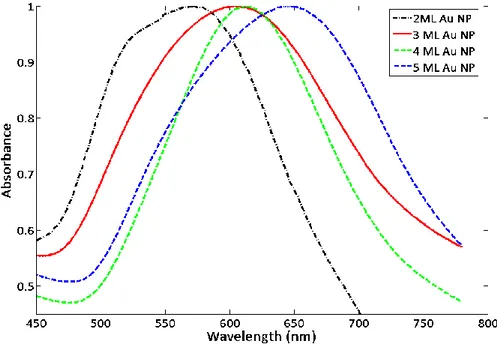
frequency [20]. Figure 2.3 shows the resonance frequency shift of our Au NPs deposited in increasing number of MLs, while effectively growing in size as metals solids.
Figure 2. 2 Resonance frequency shift of our metal nanoparticle solids growing in size.
2.5 Emission Enhancement Using Localized
Surface Plasmons
It is well known that emission of fluorescent molecules is effected by their environment as stated by Purcell in 1897. Thus it is not surprising that emission of molecules nearby metal nanoparticles is significantly altered relative to their absence [21]. Electromagnetic fields near metal nanoparticles can be significantly increased when the frequency of the incident field is in the regime of metal nanoparticles’ resonance frequency. Then this amplification may in turn increase the emission process of nearby fluorescent molecules, but it is also possible that emission of fluorescent molecules in the close proximity of metal nanoparticles can be quenched through nonradiative channels of metal nanoparticles [22]. Thus, photoluminescence of fluorescent molecules near metal nanoparticles is altered
12
depending on the absorption, emission and dissipation rates in the nanoparticles complex.
Emission of a molecule depends on both excitation rate and the ratio of radiative emission to decay rate, which is defined as quantum yield of the molecule. This relation is given in (2.6). nrad rad rad exc em (2.6)
where γexc is the total recombination rate of the emitting molecule, and γrad and
γnrad are radiative and nonradiative recombination rates.
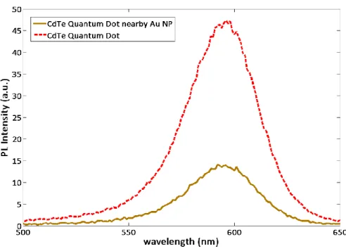
Excitation rate is mostly influenced by incident field and the angle between the direction of the field and polarization direction of the molecule. Therefore, increasing the amplitude of incident field by means of localized surface plasmon resonance can increase the excitation rate. However, the quantum yield of the fluorescent molecule can be decreased as the nonradiative decay rate can be increased due to ohmic losses for being in close proximity to metal nanoparticles. The distance between the metal nanoparticles and emitting molecules is the most critical parameter as emission enhancement or quenching of the molecule can be controlled via varying this quantity. Generally, the decrease of quantum yield is greater than increase of excitation rate and overall emission is quenched for small distances as depicted in Figure 2.4. It is also mentionable to emphasize that ohmic losses increase dramatically at the resonance frequency of the metal nanoparticle. Hence excitation wavelengths that are red shifted relative to the resonance frequency results in better emission enhancement [23].
13
Figure 2. 3 Emission quenching of our CdTe quantum dots very close to metal nanoparticles.
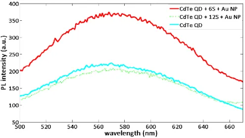
As discussed above, to achieve enhanced emission of molecules in the proximity of metal nanoparticles there should be a certain separation between them. This condition can be satisfied, for example by sandwiching dielectric layers between metal nanoparticles and fluorescent molecules. However, if the thickness of these dielectric layers is too large, then there will not be strong plasmonic coupling between the particles. This situation is depicted in Figure 2.5.
14
Figure 2. 4 Emission enhancement decreasing with increased thickness between our CdTe quantum dots and gold nanoparticles.
Size and orientation of fluorescent molecules are two other important factors apart from the distance between the molecules and the metal nanoparticles. Depending on these factors, exciton lifetime of the fluorescent molecules shortens as the energy transfer to the metal nanoparticles increases [24]. This energy transfer mechanism is nonradiative and similar to Förster resonance energy transfer that occurs between the acceptor and donor molecules. Strong coupling between excitons of fluorescent molecules and plasmons of metal nanoparticles may lead to more efficient and faster energy transfer.
Coulomb interaction is the main coupling mechanism since the distance between metal nanoparticles and fluorescent molecules is too small for treating the particles simply as dipoles while it is too far for carrier exchange to take place between the particles [25]. In this region, the exciton-plasmon coupling is strong relative to the case of large distances and exciton resonance is significantly increased as the field around the molecule is enhanced through plasmon coupling.
As illustrated in Figure 2.6(a), the distance between the metal nanoparticle and the semiconductor nanocrystal crystal is smaller than the radius of the metal nanoparticle and larger than the radius of the quantum dot. This distance is ideal
15
for strong exciton-plasmon coupling and emission enhancement. This system is excited by laser radiation which in turn stimulates both the transition dipole moment of fluorescent molecules and interband transitions of metal nanoparticles as it is depicted in Figure 2.6(b). The transition in metal nanoparticle couples to exciton in the molecule via Coulomb interaction. Thus, electric field inside the molecule is affected by laser radiation, plasmon induced field and plasmon-exciton interaction [26].
Figure 2. 5: (a) Dimensions of components and (b) coulomb interactions between a metal nanoparticle (MNP) and fluorescent molecule,e.g. semiconductor quantum dot [26].
Emission enhancement or quenching of quantum dot emitters can be better explained when the modification of radiative and non-radiative decay rates under the influence of plasmons is studied. Therefore, simple model of the basic system of Figure 2.6(a) is considered in an inductive manner by deriving equations (2.7-2.13).
In a metal-semiconductor nanoparticles complex, number of excitons in the semiconductor quantum dot is given by (2.7)
abs exc tot exc I n dt dn (2.7) where nexc is the number of excitons and γtot is total recombination rate and Iabs is
the absorption intensity inside the semiconductor.
Recombination rate of excitons in this complex is the result of three different rates, given by (2.8) metal nrad rad tot y (2.8)
16
where γrad stands for the radiative recombination rate inside the semiconductor,
γnrad is the nonradiative recombination rate and γmetal is the nonradiative decay
rate due to the nearby metal nanoparticle.
Both radiative recombination rate and absorption intensity of semiconductor nanocrystal is modified according to equations (2.9 and 2.10) when a metal nanoparticle is placed close to it.
abs exc absm P w I I ( ) (2.9) rad emis radm P w ( ) (2.10) where P(wexc) and P(wemis) are enhancement coefficients at excitation and
emission frequencies respectively. Then, emission enhancement of semiconductor nanocrystals in the proximity of metal nanoparticles can be calculated by using equation (2.11).
metal nrad rad emis tot emis exc w P w P w P E ) ( ) ( ) ( (2.11) For semiconductor nanocrystals that have a quantum yield close to 1, we have equation (2.12) and for semiconductor nanocrystals that have a quantum yield close to zero we have equation (2.13).
metal rad emis tot emis exc w P w P w P E ) ( ) ( ) ( (2.12) ) ( ) (wexc P wemis P E (2.13) Therefore, depending on the quantum yield of fluorescent molecule emission can be increased by either increasing radiative emission probability or absorption intensity.
2.6 Metal Nanoparticle Synthesis
To study plasmon coupling, we synthesized gold nanoparticles are synthesized using chemical reduction method. Materials used in this synthesis are chloroauric acid HAuCl4 and trisodium citrate Na3C6H5O7 of analytical grade
17
purity that are purchased from Sigma Aldrich of UK. First, 20 mg of chloroauric acid is taken using a plastic spoon and at this point sunlight exposure of chloroauric acid should be prevented. Then, chloroauric acid is dissolved in 100 ml of Milli-Q water using a large stirrer in a beaker while 50 mg of trisodium citrate is taken and dissolved in 5 ml of Milli-Q water using a sonicator. The beaker of chloroauric acid dissolved in water is heated until it boils and trisodium citrate is also heated in a separate beaker for preventing sudden cooling of the reaction beaker. Then, trisodium citrate dissolved in Milli-Q water is poured into the reaction beaker as the solvent inside the beaker boils. As the reaction starts, the transparency of the solution increases. After a few minutes, color of the solution turns to black and this color slowly fades to red in time. At this point, the solution is left boiling for 15 minutes and at the end of 15 minutes it reaches its final red color that looks like red wine. Finally, the solution is cooled for an hour.
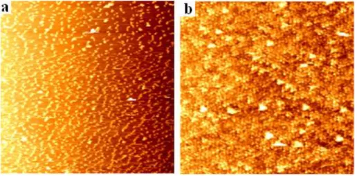
The size of the synthesized gold nanoparticles is approximately 20 nm with a 10% size distribution. We deposited them as layers of thin films using layer by layer deposition technique (as will be explained in chapter 3) and they effectively aggregate into larger solids depending on how many layers are deposited, which controls the resulting size of particles in the thin film. In Figure 2.7, atomic force microscop (AFM) graphs of 2 and 5 monolayers of thin film gold nanoparticles are given.
18
19
Chapter 3
Synthesis and Thin Film Deposition
of Colloidal Quantum Dots
Characteristic length scales that affect many physical phenomena occurring in materials are mostly in the nanometer size regime [27]. Therefore, it is expected to experience new physical phenomena that are neither revealed in molecules nor bulk form of the materials when nanoscale materials are considered.
Especially, electronic and optical properties of semiconductor nanocrystals and metal nanoparticles depend on the size of the particles. Size of the semiconductor quantum dots(QD) range from 2 to 20 nm (Figure 3.1) and varying the size of quantum dots leads to modification of their bandgap. Unlike the bulk or molecular counterparts of the semiconductor materials, this variable bandgap of quantum dots allows for tailoring optical and electronic properties of materials. This unique property of quantum dots provides an easy access to a wide range of colors. Also, when they are compared with organic fluorophores, quantum dots are much brighter and they do not photobleach. Hence, they have attracted great interest over the past two decades and research has been carried out for both physical properties and technical applications of these nanoscale materials. Today, they still attract great attention as both their shape and composition can be tailored and they can be assembled into complex structures such as supercrystals. They can be utilized as biological tags and be fabricated into devices including solar cells, lasers and light emitting diodes.
20
Figure 3. 1 Transmission electron microscope graph of a colloidal quantum dot synthesized at our nanomaterial synthesis laboratory.
3.1 Semiconductor Quantum Dots
Atoms have discrete energy states that are filled by electrons. However, as the atoms combine together to form materials, these discrete energy states forge into almost continuous energy bands such as valence and conduction bands.
Semiconductor materials have energy gaps between the valence and conduction energy bands and it is quantum mechanically forbidden for electrons to exist in this region. Photons that have energy close to the energy gap of the semiconductor or more can be absorbed and electron-hole pair (exciton) is created [28].
For bulk semiconductors, the width of the energy gap is solely determined by the composition of the material; hence, it does not change as the size of the material varies. However, size of the nanomaterial also affects the width of the energy gap and energy bands since natural length scales of electron, hole or electron-hole pair are close to the size of such quantum confined material [29]. This effect is known as the quantum size effect and these length scales can be calculated using (3.1),
21 0 *a m m aB (3.1) where a0 is the Bohr radius, ε is the dielectric constant of the medium and m and
m* are the rest and effective masses of electron and the considered particle.
Depending on how small the material is either all of the particles (electron, hole or electron-hole pair) or some of them can be confined in the boundaries of the material. Thus, three different size regimes arise as strong, weak and intermediate confinement regimes and each one of them has different effects on the structure of electronic states such as changing the shape of the energy bands and discretizing them. Nanoscale materials that exhibit this behavior are named depending on the number of confinement dimensions as quantum wires (nanorods) and quantum dots (nanocrystals). Quantum dots correspond to three dimensional confinement of the material and the width of their bandgaps is characterized by their diameters, in addition to their composition (Figure 3.2).
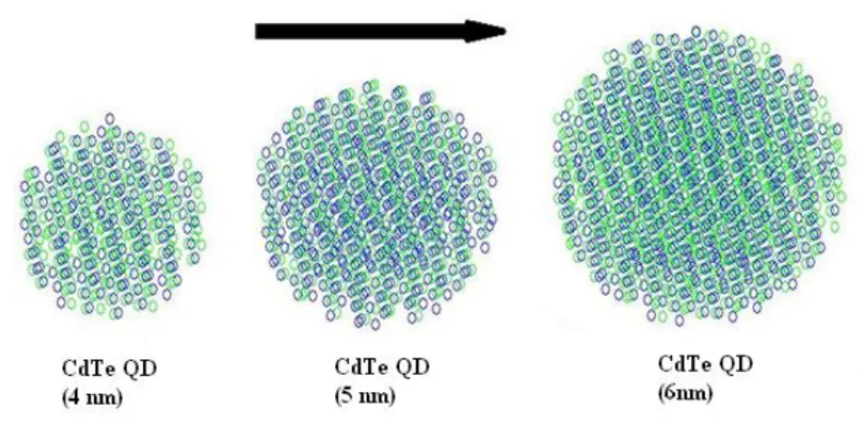
Figure 3. 2 Illustration of atom stacking CdTe quantum dots from our simulations.
As the diameter of the quantum dot decreases, strength of the quantum confinement grows stronger and the bandgap of the material increases while the continuous conduction and valence bands split into further discrete states. Even though the wavefunction of electrons and holes extends to thousands to millions of atoms, electrical response of quantum dots is discrete. Thus they can be
22
considered as quasi-atomic particles [30]. This physical phenomenon can be expressed by considering a quantum box and energy gap of the quantum dot is roughly given by (3.2): 2 2 0 4m R h E E eh g g (3.2) where Eg0 is the bandgap of the bulk semiconductor, meh is the effective electron
hole mass, h is Planck’s constant, and R is the radius of the quantum dot. or absorption intensity.
3.2 Colloidal Quantum Dot Synthesis in Aqueous
Medium
Colloidal quantum dots, also referred to as nanocrystals, are grown in solution and stabilized by a layer of surfactants via surficial attachment [31]. Prominent properties of these nanocrystals can be changed via varying size, shape and composition of core inorganic material, while stabilization, fabrication and assembly of these particles are provided by surfactants.
Colloidal nanocrystal synthesis mainly relies on the use of precursors, organic surfactants and solvents. Precursors are generally organic compounds of metals such as cadmium and common properties of precursors are fast decomposition and short reaction time. Also, the residuals of the reaction leave the medium easily.
Organic surfactants are chosen to be easily adhering molecules to nanocrystal surfaces since adhesion of surfactant is critical for determining size and shape during growth of nanocrystals. Another important property of organic surfactants is to provide dynamic solvation at the growth temperature as nanocrystals should keep growing by the addition of monomers for large sizes, while aggregation of nanocrystal cores is prevented. As the temperature decreases, these particles tend to stay in the surfaces of the nanocrystals and they
23
thus provide stability of the structure. Also, some parts of organic surfactants are responsible for solubility of the quantum dots, which determines solvents to be used.
Temperature controlled heating is important for colloidal nanocrystal synthesis. Final temperature is generally chosen in the range of 200 – 400 °C, at which both stability of organic material and melting of inorganic nanocrystals can be provided. Bulk form of CdTe melts at 1092 °C, whereas 300 °C is sufficient for nanoscale counterpart.
Colloidal nanocrystal synthesis begins with the addition of precursors and after precursors turn into chemically active monomers thorugh heating, chemical reaction is initiated and supersaturation of the medium leads to nucleation followed by the growth of nanocrystal nuclei with excess monomers.
Monomer concentration is very critical since size distribution of the syhthesized nanocrystals will eventually be set depending on this quantity. Low monomer concentration leads to broadening of size dispersion; however, low monomer concentration also enables slow growth rate due to Ostwald ripening and number of small nanocrystals shrink as they add to large nanocrystals.
Following the colloidal nanocrystal synthesis, several methods such as size selective precipitation are used for narrowing down the size distribution. It is also possible to achieve simultaneous growth of small nanocrystals by means of rapid injection. But slow growth rate is generally preferred for obtaining nearly spherical and large nanocrystals. At the end of colloidal synthesis, considerable amount of monomers are placed on the surface of NCs and an interface of inorganic-organic layer is formed.
Achieving monodispersive nanocrystals by means of size, shape, crystal structure and surficial property is necessary for studying physical properties of these particles. Most of the nanocrystals synthesized have size in the range of
2-24
10 nm, where both mean value and standard deviation of size can be precisely predefined similar to the synthesis of polymers. Two decades of progress has been leading nanocrystal synthesis of well-defined structures. Methods used for synthesis include coprecipitation in aqueous phase, using reverse micelles as templates, solvothermal synthesis, hydrothermal synthesis and hot injection [32, 33].
We synthesize CdTe quantum dots in aqueous medium at our nanomaterial synthesis laboratory using hot injection method. Materials used in this synthesis are aluminum telluride (Al2Te3) and cadmium perchlorate hexahydrate
(Cd(ClO4)26H2O) as precursors, thioglycloic acid (TGA: (SH)CH2COOH) as
the organic surfactant, Milli-Q water, sodium hydroxide (NaOH), sulfuric acid (H2SO4) and iso-propanol (C3H7OH) as solvents and such.
In Step 1, 4.59 gram cadmium perchlorate hexahydrate and 250 ml Milli-Q water are mixed in a 1l round bottom 3-neck reaction flask and the mixture is stirred with a magnetic stirrer vigorously until all of the cadmium perchlorate hexahydrate is dissolved in water as the solution becomes transparent.
In Step 2, 250 ml Milli-Q water is added in small amounts into a small vial containing 1.33 gram thioglycloic acid. Then, the mixture is poured into the large flask containing cadmium perchlorate hexahydrate and 250 ml Milli-Q water solution. This step continues until no smell of thioglycloic acid is detected from the small vial. Finally, rest of the Milli-Q water is poured into the large flask.
In Step 3, pH value of reaction flask is adjusted by adding NaOH solution slowly since after some drops pH value grows dramatically. At the end, the pH value of the reaction flask should lie between 11.8 and 12.0.
25
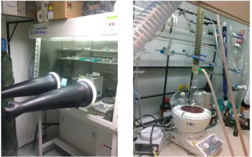
In Step 4, 800 mg of aluminum telluride is taken into a 25 ml 3-neck flask in the glove box (Figure 3.2). All the necks of the flask are covered with either septa or parafilm in order to prevent aluminum telluride from oxidizing.
Figure 3. 3 Our glove box and experimental synthesis setup in the fume hood.
In Step 5, 0.5 molar H2SO4 solution is prepared for later use and the following
setup is assembled. Argon is flowed through the system for approximately one hour to remove all the O2 in the system.
In Step 6, H2SO4 is taken by a syringe and dropped into the small flask containing
aluminum telluride through the septum closing the neck. As the reaction takes place, H2Te gas is generated and carried to the large flask via argon flow in the
system. After half an hour, small flask is separated from the large flask and the neck of large flask is closed again.
In Step 7, heating mantle is placed under the reaction flask and the flask is heated for boiling the mixture inside. At this boiling temperature, CdTe quantum dot growth begins. As the size of the quantum dots increases, their emission color shifts to longer wavelengths (Figure 3.3).
26
In the final step, either small aliquot can be taken for checking the growth of quantum dots as time passes or the reaction is stopped by cooling the system when the synthesized CdTe quantum dots reach the targeted diameters. Then, the solution is filtered to remove the remnants of the reaction. Finally, to obtain monodisperse quantum dots size selective precipitation methods are applied.
Figure 3. 4 Color variation of our CdTe quantum dots at our nanomaterial synthesis laboratory.
3.3 RF Characterization of Colloidal Quantum
Dots
To measure QD dipole moments, we designed and fabricated a micrometer-scale on-chip measurement setup in parallel plate capacitor architecture. The two electrode plates, made of Ti/Au layers, were microfabricated on a Si substrate. The spacing between the plates was set to be 70 µm with a lateral housing of 1 cm2 in cross-sectional area to place our QDs in solution. TOPO-capped QDs, as shown in Figure 1(a), were prepared using ligand exchange, for TOPO does not affect RF measurements. The external bias applied across the plates that house our TOPO-capped QDs in solution enforces alignment of QDs as sketched in Figure 3.5(a).
27
Figure 3. 5 (a) TOPO-capped CdSe QD (with only one TOPO ligand shown in the sketch for the sake of clarity) and (b) alignment of QDs when an external bias is applied across
the plates of the microfabricated on-chip setup.
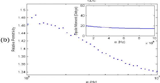
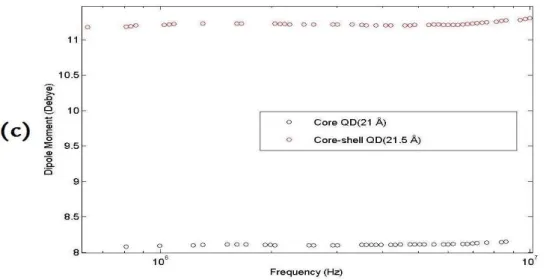
We implemented two different methods to measure dipole moment of our QDs. One of them relies on measuring capacitance as a function of operating frequency by an impedance analyzer (IA), whereas the other one is based on taking S-parameter spectral measurements by a programmable network analyzer (PNA). In both of these methods, the measurements were performed before and after the QDs were placed in the housing. As a result, we determined the relative dielectric constant dispersion by normalizing each measurement in the presence of QDs to that in the absence of QDs. Using several equations including Claussi-Mosotti equation we obtained the dipole moments of CdSe QDs in three different sizes and a pair of CdSe core and CdSe-ZnS core-shell QDs of similar size.
Figures 3.6, 3.7 and 3.8 represent the experimental data obtained using both IA and PNA. The results of these two independent measurements are in good agreement. Here we observed that 1.) the dipole moments of these CdSe QDs are proportional to their sizes, 2.) their dipole moments do not show dramatic changes over a wide range of operating frequency characterized in our experiments, and 3.) core-shell structure shows greater dipole moment than only core structure of similar size. Currently, further experiments are underway to understand the increased dipole moment in core-shell structures as opposed to only core structures. Therefore, we measured the dipole moments of CdSe QDs synthesized in different sizes and structures by implementing two different RF measurement methods, one using impedance analyzer and the other using programmable network analyzer.
28
Figure 3. 6 Dipole moment of TOPO-capped CdSe QDs in different sizes (27 Å, 36 Å, and 53Å) measured as a function of operating frequency by impedance analyzer.
Figure 3. 7 Relative permittivity and dipole moment (in the inset) of TOPO-capped CdSe QD (27 Å) measured as a function of operating frequency by programmable network
29
Figure 3. 8 Dipole moments of TOPO-capped CdSe core QD (21 Å) and CdSe-ZnS core-shell QD (21.5 Å) measured as a function of operating frequency by programmable
network analyzer.
3.4 Optical Characterization of Colloidal
Quantum Dots
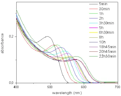
We make the optical characterization of colloidal quantum dots in either solution or film using Cary UV-VIS spectrophotometer to record absorbance spectra and Cary Eclipse fluorescence spectrophotometer to take photoluminescence spectra. Absorbance spectra of our synthesized CdTe quantum dots of varying sizes are shown in Figure 3.9.
30
Figure 3. 9 Absorption spectra of our CdTe quantum dots of varying size controlled by reaction growth time (from 5 min. to 22 h. 30 min.).
As the absorbance spectra of CdTe quantum dots in Figure 3.9 illustrates the first exciton absorption peak of quantum dots shifts to longer wavelengths if their growth time increases. This observation is a natural result of the fact that the bandgap of quantum dots decreases as their size thereby grows and less energetic photons make optical transitions across their effective bandgap at longer wavelengths. It should be also noted that for further shift of the first exciton absorption peak much longer time of growth is necessary. This is inevitable because Oswald ripening, which enables the growth of quantum dots is a slow process even requiring several days [34].
The data obtained from these absorbance spectra can be used to find either extinction coefficient or concentration of quantum dots in solution by using Lambert-Beer’s law if one of the two is known [35]. For thin films of quantum dots relative concentrations of particles can be obtained by calculating the areas under the absorbance spectra and rating them with respect to each other.
31
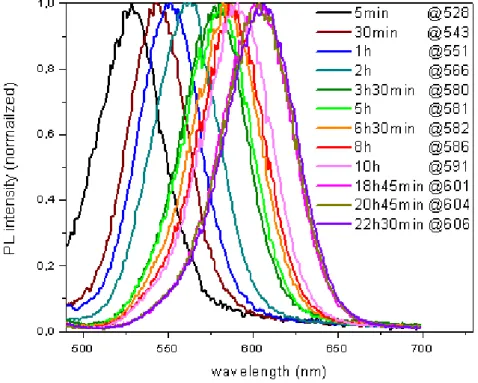
Photoluminescence spectra of our synthesized CdTe quantum dots are shown in Figure 3.10. As in photoluminescence is the case in the absorbance spectra of these quantum dots, the peak position of the curves in Figure 3.10 also shifts to longer wavelengths as the growth time increases. This observation can also be explained with the same reasoning.
Figure 3. 10 Photoluminescence spectra of our CdTe quantum dots of varying size controlled by growth time (from 5 min. to 22 h. 30 min.).
Exciton lifetime measurements are conducted using our time-resolved fluorescence setup (picoquant). Photoluminescence decay curves of CdTe quantum dots emitting in green and red are compared in Figure 3.11. As can be seen from the figure, green emitting CdTe (560 nm) quantum dots have shorter exciton lifetimes than red emitting CdTe (640 nm) quantum dots. This observation is expected since quantum dots with larger bandgaps (or larger transition dipole moments) decay faster [36]. Also, quantum dot photoluminescence intensities at peak wavelengths can be compared by using this setup in constant time mode.
32
Figure 3. 11 Time-resolved fluorescence spectra of our CdTe quantum dots with two different sizes (emitting at 560 and 640 nm peak wavelengths).
3.5 Colloidal Quantum Dot Thin Film Deposition
Nonradiative energy transfer mechanism mainly depends on the distance between the interacting molecules. Therefore, fabrication techniques that enable controlled separation between different types of molecules are extremely important. Several methods including Langmuir-Blodgett and self-assembly are used to fabricate monolayer and multilayer films over the past few decades [37]. Layer by layer deposition technique is developed at early nineties and offers a simpler assembly approach for developing multilayer films relatively less dependent of the substrate size and topology on which they grow [38]. This method utilizes electrostatic attraction forces between oppositely charged layers hence positively and negatively capped layers are deposited one after another in the desired construction. In Figure 3.12, subsequent deposition of pairs of positively and negatively charged polymers and positively charged polymer and negatively charged nanoparticles starting over negatively charge glass substrate is depicted.
33
Figure 3. 12 Deposition of positively and negatively charged layers using layer by layer deposition technique.
Layer by layer deposition method starts with the deposition of a positively charged polymer layer on top of a substrate whose surface is negatively charged and is followed by a washing step for cleaning the sample from excessive polymer that is not properly adhered via Coulomb attraction. Next step is the deposition of negatively charged polymers or particles followed by a washing step again. In this cyclic manner, deposition of tens of layers is possible. The process flow of layer by layer deposition technique is illustrated in the Figure 3.13.
34
We use this deposition technique for fabricating multilayer films of quantum dots and metal nanoparticles with precisely controlled nanoscale spacing between them. First, surface treatment of glass slides that have nanoscale roughness on their surfaces is carried out by vibrating them in sonicator for approximately ten minutes in solutions of sodium hydroxide (NaOH), methanol (CH3OH), acetone
((CH3)2CO) and iso-propanol(C3H7OH) in turn. By doing so, surfaces of the glass
slides are negatively charged [39]. We use polydiallyldimethylammonium chloride (PDDA) as polyanion and sodium4-styrenesulfonate (PSS) as polycation to form polyelectrolyte bilayers. Both PDDA of 300 µl and 30 grams of PSS are dissolved in Milli-Q water that has 0.1M salt (NaCl) initially dissolved in it. Salt is used in these solutions because it provides swelling and breaks excessive bounds between PDDA and PSS and more homogeneous thin films are obtained [40]. Also, CdTe quantum dots are solved in salted Milli-Q water. Subsequently, repeated deposition of desired layers is conducted by a computerized dip coating system (manufactured by Nima Technology, UK) in a process program set with critical parameters including durations and speeds of immersing, withdrawing and holding in solution, which are optimized iteratively for our purposes.
Figure 3. 14 Scanning electron microscop graph of our thin film CdTe quantum dot solids deposited by layer-by-layer assembly technique.