c
⃝ T¨UB˙ITAK doi:10.3906/fiz-1801-1 h t t p : / / j o u r n a l s . t u b i t a k . g o v . t r / p h y s i c s /
Research Article
Chemical vapor transport synthesis of a selenium-based two-dimensional material
Talip Serkan KASIRGA1,2,3,∗
1National Nanotechnology Research Center (UNAM), Bilkent University, Bilkent, Ankara, Turkey 2
Institute of Materials Science and Nanotechnology, Bilkent University, Bilkent, Ankara, Turkey
3Department of Physics, Faculty of Science, Bilkent University, Bilkent, Ankara, Turkey
Received: 02.01.2018 • Accepted/Published Online: 10.04.2018 • Final Version: 01.06.2018
Abstract: Selenium-based layered materials, and in particular transition-metal diselenides (TMDSs), have intriguing
properties in the monolayer limit. Materials such as MoSe2, WSe2, and NbSe2 display striking features such as
spin-valley coupling at the valence-band edges and offer great potential for optoelectronics applications. Although a dozen of other TMDSs have been realized or proposed, whether two-dimensional chalcogens are possible or not is still an open challenge. In this work, we show the chemical vapor transport synthesis of a novel, atomically thin selenium-based material on oxidized silicon substrates. This new member of the two-dimensional materials family has a unique Raman spectrum similar to that of bulk selenium and has an optical gap of ∼1.57 eV at room temperature determined by the photoluminescence. No transition metals are found in the stoichiometry of the crystals. Analysis of high-resolution transmission electron micrographs of the monolayers reveals a distinctive set of hexagonal spots indicating a sixfold symmetry of the lattice. Atomic force microscopy measurements show the monolayer thickness to be ∼0.75 nm.
Key words: Selenium-based monolayer, 2D materials, chemical vapor transport, atomically thin materials
1. Introduction
Atomically thin two-dimensional (2D) materials offer exciting possibilities in electronics and optics [1–3]. Many anticipated members of the 2D materials family, from group III to group V [4–7] elements as well as compounds of transition metals with chalcogens, have now been synthesized or isolated with various electrical properties [8]. Degrees of freedom other than the electronic charge such as electronic spin [9,10] and valley polarization [11,12] also offer physics that would be inaccessible by many measurement techniques in bulk materials. It is also possible to produce tailored van der Waals stacks of these atomically thin materials to have unprecedented functionality [8,13,14].
So far, 2D allotropes of various elements have been discovered [15]. Silicence [16], phosphorene [17], germanene [18], stanene [19], borophene [20], and antimonene [21] are some of the recently synthesized elemental 2D materials. All of the monolayers of such elemental 2D materials are unstable under ambient conditions. Although group VI elements contribute to the formation of 2D structures, the existence of stable 2D structures of group VI elements remains largely unexplored [22]. Group VI elements typically have stable crystals with helical chains parallel to the c-axis in a trigonal crystal system. For this reason, elongated nanocrystals such as nanobelts [23] and nanorods [24] of group VI elements are more commonly synthesized [25]. It is unclear whether
KASIRGA/Turk J Phys
2D structures of group VI elements are possible or not. In this work, we introduce a novel selenium-based 2D structure that might be relevant to the 2D allotrope of selenium.
2. Materials and methods
Details of the monolayer synthesis are given in the main text. AFM scans are taken with a Park Systems XE-100. More than ten thin flakes are scanned for thickness. We obtain values ranging from 0.56 to 0.81 nm for monolayers and 1.30 to 1.55 nm for bilayers. In the text, we report the most observed value, 0.75 nm. For XPS measurements K-Alpha from Thermo Scientific is used. The X-ray spot size on the sample is adjusted to 100 µ m in diameter. For Raman and PL measurements a custom-made setup as well as a Witec Alpha 300 are used. In both setups a 532 nm laser is utilized as the excitation source. TEM measurements are taken using an FEI Tecnai G30. TEM samples are prepared by transferring monolayers onto custom TEM grids using the cellulose acetate butyrate (CAB) polymer transfer method [26].
3. Results
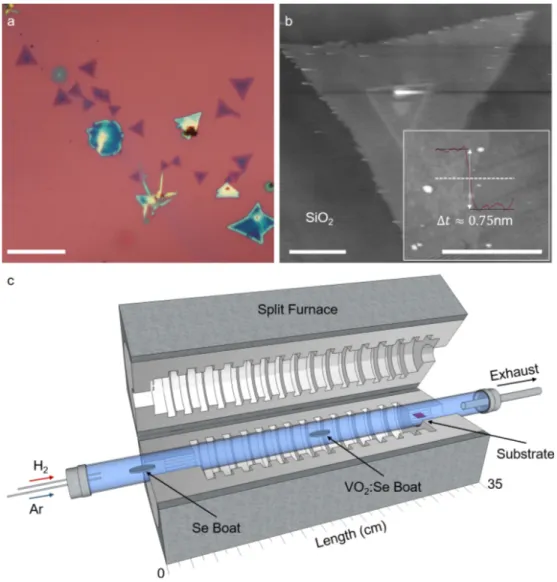
We investigate the compositional and the structural properties of the chemical vapor transport (CVT) synthe-sized monolayer crystals. Our results presented here show that there are no measurable traces of transition metals in the structure of the monolayers, and they are composed of selenium. An optical microscope image of typical crystals grown on a silicon wafer with 280 nm oxide is shown in Figure 1a. The atomic force microscopy (AFM) scan over a triangular crystal is given in Figure 1b, which shows the monolayer thickness to be ∼0.75 nm. The monolayer thickness indicates that the crystal might have a buckled structure as in the case of black phosphorous.
The atmospheric pressure CVT setup we use to synthesize the crystals is based on a single-zone tube furnace with hydrogen (5 N purity) and argon (5 N purity) gas inlets separately controlled by mass flow controllers (MFCs). Selenium (Alfa Aesar, A12592) and vanadium dioxide (VO2) powders (Alfa Aesar, 22957) are used to perform the growth. Both powder sources are placed in dedicated alumina boats. We add Se powder into the VO2 boat as well, typically in a 2:1 VO2:Se ratio. We use the same VO2 powder for more than five growths while adding Se in the specified ratio before each growth. Using the same powder over many growths seems to improve the monolayer yield. However, after a certain number of growths, the yield starts dropping and we replenish the VO2 powder. The role of VO2 in the synthesis is not clear to us at the moment. When VO2 is not added to the central boat, we do not get monolayer growth.
The boats and the substrates are loaded in an inner tube (quartz) in precise locations and the inner tube is slid into the fixed outer tube (quartz) through the flange opening. Temperature distribution throughout the length of the furnace is known in 5 mm steps for various furnace center temperature set points. The source materials and the substrate are placed accordingly into the tube to match the desired temperature. The selenium boat is placed upstream towards the outer rim of the heat shield of the furnace, where the temperatures are at 20% of the center of the furnace. This placement is to ensure that the selenium source stays in the liquid phase for the entire duration of the growth. The VO2 boat is placed in the center where the temperature is the highest within the furnace. A schematic of the CVT setup is given in Figure 1c.
The crystals are grown on a 280 nm oxidized Si wafer substrate. The substrate is rinsed with deionized water and the water droplets are left on the substrate intentionally. Then the substrate is baked for 10 min on a preheated hotplate at 120 ◦C. We note that after baking the substrate there are circular drying stains on the substrate. After the growth, the monolayers mostly form around these drying stains. The substrate is
Figure 1. a) Optical microscope image of typical triangular crystals of the synthesized material is shown. Some of the
crystals seen here have more than a single layer. Scale bar is 20 µ m. b) AFM scan over a crystal shows that the layer thickness is about 0.75 nm. The inset shows a line trace taken along the dashed line across the edge of a monolayer. Scale bar is 5 µ m for the main image and 1 µ m for the inset. c) Schematic of the CVT setup shows the typical placement of the source boats and the substrate within the furnace. The setup operates at atmospheric pressure while the ambient condition within the tube is controlled by MFCs that regulate Ar and H2 flows. Relevant dimensions of the furnace
schematic are in scale.
placed within the heat shield region of the furnace where the temperature is roughly at 60% of the center of the furnace. The growth starts by purging the furnace with 500 sccm Ar for 10 min. For the first 5 min of the purging, 100 sccm H2 is passed through the tubing as well in order to ensure that the tubing is free of air. Then the furnace is powered up to reach 920 ◦C at a rate of 25 ◦C/min while maintaining a 4 sccm Ar flow. When the center zone temperature reaches 920 ◦C, the gas mixture is introduced at a rate of 80:10 sccm Ar:H2 for 5 min. After 5 min, the power turns off as programmed and the center zone temperature drops to about 750 ◦C in 1 min. Finally, the lid of the furnace is opened at 750 ◦C to quench the synthesis. During this rapid cool-down period, only 6 sccm Ar gas flows to keep a positive pressure inside the tube. The growth method yields a typical monolayer size of ∼5 µm and the monolayers are scarcely distributed, mostly around
KASIRGA/Turk J Phys
the aforementioned drying stains. We would like to add that the monolayer growth takes place at various center temperatures ranging from 890 to 940 ◦C.
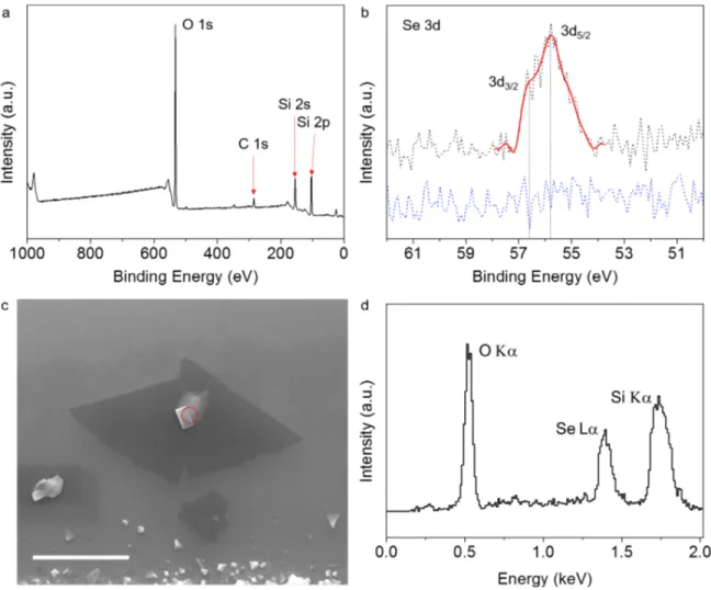
X-ray photoelectron spectroscopy (XPS) surveys are conducted on various samples to analyze the ele-mental content of the thin flakes right after the growth. Due to very small surface coverage of the monolayers on the substrate, the XPS signal resulting from them is very dim. However, the results show that the surface of the substrate with monolayers contains Se, Si, O, and C (Figure 2a). As the substrate is an oxidized silicon chip, Si and O have very bright peaks. XPS surveys of four different samples show no traces of vanadium or any other transition metals. Figure 2b shows a typical XPS survey for the Se 3d binding energy taken from both a region of the sample with the monolayers (black dotted line) and a different region without the monolayers (blue dotted line). The latter indicates that there is no selenium film formation on the substrate and the signal is indeed resulting from the monolayers. The signal is localized around 56 eV and the line fitting of the spectrum (red solid line) reveals that the signal is composed of two closely spaced peaks, Se 3d5/2 and 3d3/2, separated by 0.81 eV. This spin-orbit splitting value is similar to the values reported in the literature for Se [27]. The binding energies of selenides are typically around 55 eV or even less [28] and selenium oxides are above 59 eV. Thus, based on the XPS spectra we conclude that the monolayers and the growth around them are mostly composed of selenium.
Although the main feature of the substrate is the monolayer material, various three-dimensional (3D) structures often occur on or around the monolayers. A scanning electron microscopy (SEM) micrograph of a typical example is shown in Figure 2c. Energy dispersive X-ray (EDX) measurements of these three-dimensional features indicate a result similar to the XPS surveys on the monolayers. A majority of the signal comes from Si, O, and Se (Figure 2d) and no transition metals, in particular vanadium, appear in the EDX spectra analysis. We expect to see Si and O since EDX is not a surface-sensitive technique, and X-rays created within the substrate are also measured. We think that these structures could act as seeds for the 2D growth. One plausible route might be through formation of selenium dioxide with the oxygen provided from the VO2 source during the ramp-up. Once the growth temperature is achieved, reduction of selenium dioxide with hydrogen takes place to form the 2D crystals. Further investigation is required to elucidate the growth mechanism.
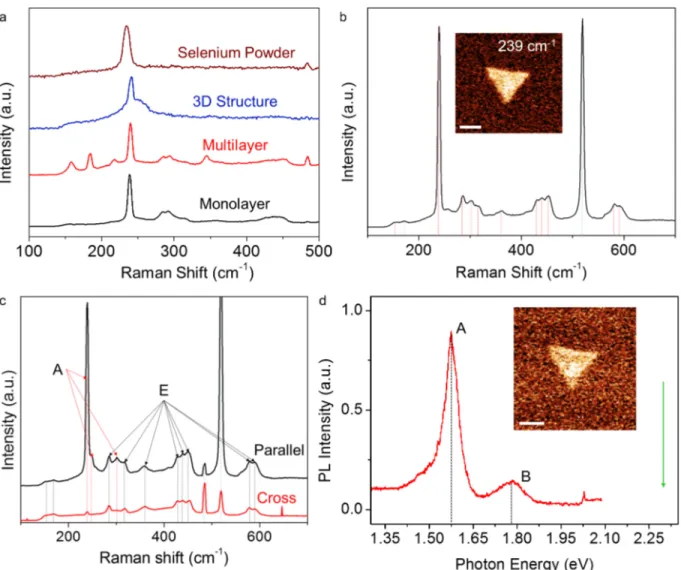
The Raman spectrum of monolayers has a unique set of peaks. We performed Raman spectroscopy using a diffraction-limited confocal microscope with 532 nm laser. Figure 3a shows the spectra taken on various crystal forms seen on the substrate as well as the selenium powder precursor used in the CVT growth. Although slightly shifted among the various forms, the peak around 239 cm−1 is the dominant Raman mode in all spectra. Figure 3b shows a more detailed scan taken on a monolayer sample. The inset in Figure 3b is an integrated intensity map of the 239 cm−1 peak. The characteristic phonon vibrational mode, A1, of the Se helical chains in trigonal selenium (t-Se) at 237 cm−1 is strikingly close to the 239 cm−1 that we measure in our monolayers [29]. There are many other peaks that we associate with the monolayers, marked by a red dashed line in the graph [30]. When we compare these peaks to that of SeO2, especially the peaks that are attributed to Eg, A1g, and B2g show similar frequencies [31]. However, SeO2 has no Raman active vibrational modes in the 400–500 cm−1 frequency range while our monolayers have three peaks in this range. These modes coincide with the Raman peaks of t-Se [32,33].
To understand the origin of the Raman active modes, polarization-dependent Raman spectroscopy is performed on the monolayers. Figure 3c shows the spectra for parallel z(xx)¯z and cross z(xy)¯z polarization
configura-Figure 2. a) XPS survey taken over a region of a typical sample with monolayers, with 100 µ m diameter X-ray spot
size. Majority of the peaks belong to O, Si, and C. The peaks that belong to these elements are labeled on the graph. As the surface coverage of the crystals is very small, the Se peak is very dim. b) Se 3d peak is centered at around 55.9 eV (black dotted line) and smoothing of the data (red solid line) shows that the peak is composed of two peaks belonging to Se 3d5/2 and 3d3/2. To ensure that the signal is coming from the monolayers, we took an XPS survey from a region of
the substrate with no monolayers and the Se 3d peak vanishes (blue dotted line). c) SEM image of a typical monolayer with a bulk crystal formation on top. Red dashed circle indicates the region where the EDX spectrum is taken from. Scale bar is 4 µ m. d) EDX spectrum shows that there are no elements except O, Se, and Si. Bright Si and O peaks are expected in the signal as EDX is not a surface-sensitive technique and some portion of the signal comes from the substrate.
tion, indicating that it is an A mode. A and E Raman active vibrational modes that are associated with the measured peaks are indicated on the graph. Here, we do the mode labeling based on the observation that the monolayers have a hexagonal symmetry as discussed later in the text when we discuss the transmission electron microscopy (TEM) results.
Using the same setup we use for Raman measurements, we have looked for the photoluminescence (PL) spectra of the monolayers at room temperature. Figure 3d shows the PL spectrum taken from a monolayer flake and the inset shows the PL intensity map integrated around 1.77 eV, from the flake. There are two distinct PL
KASIRGA/Turk J Phys
Figure 3. a) Raman spectra taken from selenium powder used in the growth, 3D structure of the monolayers, multilayer,
and monolayer crystals are given. Strikingly the peak around 239 cm−1 appears in all four forms with a slight shift. b) A more detailed spectrum for the monolayer sample is given. Red dashed lines indicate the peaks that are associated with the monolayer while the blue dashed line is the Si 520 cm−1 peak. The inset shows the intensity map integrated around the 239 cm−1 peak. Scale bar is 2 µ m. c) Polarization-dependent Raman spectra for the monolayer sample show that for parallel and cross polarized detection intensities of the 239 cm−1 peak and two other peaks indicated by red dashed lines differ. A and E vibrational modes are indicated based on the polarization dependence. d) Photoluminescence spectrum shows two major peaks separated from each other by 200 meV. The lower energy peak emerges from the A excitons and the higher energy dimmer peak comes from the B excitons. We note that there is a slight shoulder to the A peak towards lower energies. Green arrow indicates the excitation energy. The inset shows an intensity-integrated map of the B exciton peak. Scale bar is 2 µ m.
peaks separated by 200 meV. The dimmer peak is centered at around 1.77 eV and the brighter peak at around 1.57 eV. The peak at 1.57 eV has a width of ∼60 meV, and we consider this peak to emerge from A excitons. The other peak at 1.77 eV can be attributed to B excitons [34]. Slight broadening of the A peak towards lower energies could indicate formation of charged excitons by n-type doping due to the charge transfer from the SiO2 substrate [35]. Based on the PL measurements, the synthesized monolayers have semiconducting behavior with
an optical gap of 1.57 eV. We would like to note that for the bulk t-Se the band gap is reported to be 1.6 eV, while this value increases in nanowires up to 1.76 eV [24].
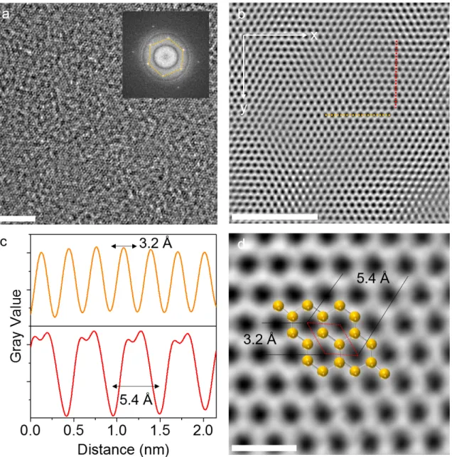
Finally, we performed TEM studies to determine the crystal structure. We would like to note that even with low electron beam energies, the monolayers quickly deteriorate due to the electron beam, making
Figure 4. a) HR-TEM image of a free-standing monolayer. The inset shows the FFT of the HR-TEM image. Although
the image is blurry due to the polymer residue on the surface and rippling of the monolayer, the FFT reveals a sixfold symmetric structure with interplanar spacing of 2.77 ˚A between the (100) planes. Scale bars show 4 nm in length. b) The inverse transform image from the filtered FFT clearly shows the honeycomb lattice of the monolayer. The x and y directions indicated on the image are arbitrary directions. Scale bar is 4 nm. c) Intensity profiles along the red and yellow dashed lines in 4b are shown here. The upper panel is for the profile along the dashed line (yellow) in the x direction and the lower panel is for the profile along the dashed line (red) in the y direction. d) A zoomed-in inverse FFT with depicted selenium atoms overlaid. The primitive cell is denoted with a red dashed parallelogram. Scale bar is 0.5 nm.
KASIRGA/Turk J Phys
it extremely difficult to get high quality images, EDX, and electron energy loss spectra (EELS). A similar case for Se nanoribbons was reported in the literature and it was attributed to the low melting point of Se [36]. High-resolution transmission electron microscopy (HR-TEM) measurements are performed on monolayers transferred on custom-made Si3N4 TEM grids. An exemplary HR-TEM image is given in Figure 4a. The fast Fourier transform (FFT) generated from the HR-TEM image shows a sixfold symmetric structure with an interplanar spacing of 2.77 ˚A between the (100) planes (Figure 4a, inset). An inverse transform of the filtered FFT image reveals the hexagonal structure as shown in Figure 4b. This crystal structure is different than that of t-Se. Thus, we consider the monolayers to be an allotrope of selenium. Intensity profiles taken through the center of the hexagons along the x and y directions (indicated on the image) show a uniform gray value for the peaks (Figure 4c). The separation between the troughs along both directions show that the primitive cell parallelogram has a 3.2 ˚A side and a 5.4 ˚A diagonal as depicted in Figure 4d.
4. Discussion
In conclusion, we report a novel 2D material synthesized by CVT. The monolayers have a sixfold symmetric crystal structure and the monolayer thickness is ∼0.75 nm. The monolayer thickness indicates that the crystal might have a buckled structure, as in the case of black phosphorous. However, unlike other elemental 2D materials, our monolayers are stable under ambient conditions for several months. This novel material exhibits a unique Raman spectrum. XPS and EDX surveys reveal that the material is mostly composed of Se. One plausible stoichiometry we considered was SiSe2. The low-temperature polymorph of SiSe2, denoted as SiSe2 -400, is known to form a 2D layered structure [37]. However, the Raman spectra of bulk layered SiSe2 do not match with our measurements and under ambient conditions SiSe2 is highly sensitive to moisture; it degrades rapidly by forming hydrogen selenide [38,39]. Thus, we rule out the possibility of SiSe2 as a plausible candidate for our crystals. Still, the evidence we provide in this paper shows that the synthesized monolayer crystals are likely to be a 2D allotrope of selenium, selenene. However, density functional theory calculations show a different stable crystal structure than what we observe in SEM measurements and so far no stable hexagonal lattice has been reported for selenene [22]. We believe that this work could have an impact on the investigation of novel 2D materials, especially in the studies of 2D structures of chalcogens.
Acknowledgments
This work was supported by the Scientific and Technological Research Council of Turkey (T ¨UB˙ITAK), 1001-Project No: 214M109. I would like to thank Mehdi Ramezani, Mustafa Fadlelmulla, and Engin Can S¨urmeli for their help with some of the measurements.
References
[1] Chhowalla, M.; Jena, D.; Zhang, H. Nat. Rev. Mater., 2016, 1, 16052.
[2] Schaibley, J. R.; Yu, H,; Clark, G.; Rivera, P.; Ross, J. S.; Seyler, K. L.; Yao, W.; Xu, X. Nat. Rev. Mater. 2016, 1, 16055.
[3] Jariwala, D.; Marks, T. J.; Hersam, M. C. Nat. Mater. 2017, 16, 170-181. [4] Wallace, P. R. Phys. Rev. 1947, 71, 622-634.
[5] Ataca, C.; S¸ahin, H.; Ciraci, S. J. Phys. Chem. C 2012, 116, 8983-8999.
[7] Piazza, Z. A.; Hu, H. S.; Li, W. L.; Zhao, Y. F.; Li, J.; Wang, L. S. Nat. Commun. 2014, 5, 3113. [8] Geim, A. K.; Grigorieva, I. V. Nature 2013, 499, 419-425.
[9] Zhu, Z. Y.; Cheng, Y. C.; Schwingenschl¨ogl, U. Phys. Rev. B 2011, 84, 153402. [10] Xiao, D.; Liu, G. B.; Feng, W.; Xu, X.; Yao, W. Phys. Rev. Lett. 2012, 108, 196802. [11] Rycerz, A.; Tworzyd lo, J.; Beenakker, C. W. J. Nat. Phys. 2007, 3, 172-175. [12] Mak, K. F.; He, K.; Shan, J.; Heinz, T. F. Nat. Nanotechnol. 2012, 7, 494-498. [13] Fogler, M. M.; Butov, L. V.; Novoselov, K. S. Nat. Commun. 2014, 5, 4555.
[14] Novoselov, K. S.; Mishchenko, A.; Carvalho, A.; Neto, A. H. C. Science 2016, 353, aac9439. [15] Mannix, A. J.; Kiraly, B.; Hersam, M. C.; Guisinger, N. P. Nature Rev. Chem. 2017, 1, 0014.
[16] Vogt, P.; Padova, P. D.; Quaresima, C.; Avila, J.; Frantzeskakis, E.; Asensio, M. C.; Resta, A.; Ealet, B.; Lay, G. L. Phys. Rev. Lett. 2012, 108, 155501.
[17] Liu, H.; Neal, A. T.; Zhu, Z.; Luo, Z.; Xu, X.; Tom´anek, D.; Ye, P. D. ACS Nano 2014, 8, 4033-4041.
[18] Li, L.; Lu, S. Z.; Pan, J.; Qin, Z.; Wang, Y. Q.; Wang, Y.; Cao, G. Y.; Du, S.; Gao, H. J. Adv. Mater. 2014, 26, 4820-4824.
[19] Zhu, F. F.; Chen, W. J.; Xu, Y.; Gao, C. L.; Guan, D. D.; Liu, C. H.; Qian, D.; Zhang, S. C.; Jia, J. F. Nat. Mater.
2015, 14, 1020-1025.
[20] Mannix, A. J.; Zhou, X. F.; Kiraly, B.; Wood, J. D.; Alducin, D.; Myers, B. D.; Liu, X.; Fisher, B. L.; Santiago, U.; Guest, J. R. et al. Science 2015, 350, 1513-1516.
[21] Ji, J.; Song, X.; Liu, J.; Yan, Z.; Huo, C.; Zhang, S.; Su, M.; Liao, L.; Wang, W.; Ni, Z. et al. Nat. Commun. 2016, 7, 13352.
[22] Xian, L.; Paz, A. P.; Bianco, E.; Ajayan, P. M.; Rubio, A. 2D Mater. 2017, 4, 041003. [23] Ma, Y.; Qi, L.; Shen, W. Ma, J. Langmuir 2005, 21, 6161-6164.
[24] Gates, B.; Mayers, B.; Grossman, A.; Xia, Y. Adv. Mater. 2002, 14, 1749-1752. [25] Hu, J.; Odom, T. W.; Lieber, C. M. Accounts Chem. Res. 1999, 32, 435-445.
[26] Schneider, G. F.; Calado, V. E.; Zandbergen, H.; Vandersypen, M. K.; Dekker, C. Nano Lett. 2010, 10, 1912-1916. [27] Moulder, J. F.; Stickle, N. F.; Sobol, P. E.; Bomben, K. D., Eds. Handbook of X-ray Photoelectron Spectroscopy;
Physical Electronics Inc.: Eden Prairie, MN, USA, 1995.
[28] Zhao, W.; Dong, B.; Guo, Z.; Su, G.; Gao, R.; Wang, W.; Cao, L. Chem. Commun. 2016, 52, 9228-9231. [29] Sinha, A. K.; Sasmal, A. K.; Mehetor, S. K.; Pradhan, M.; Pal, T. Chem. Commun. 2014, 50, 15733-15736. [30] Cooper, W. C. The Physics of Selenium and Tellurium; Pergamon Press: Dorking, UK, 1967.
[31] Anderson, A.; Sanders, A.; Smith, W. J. Raman Spectrosc. 2000, 31, 403-406. [32] Nagata, K; Ishikawa, T.; Miyamoto, Y. Jpn. J. Appl. Phys. 1983, 22, 1129. [33] Yu, P. Y.; Amer, N.; Shen, Y. R.; Petroff, Y. Phys. Rev. B 1976, 14, 644-652. [34] Coehoorn, R.; Haas, C.; Groot, R. A. D. Phys. Rev. B 1987, 35, 6203-6206.
[35] Scheuschner, N.; Ochedowski, O.; Kaulitz, A. M.; Gillen, R.; Schleberger, M.; Maultzsch, J. Phys. Rev. B 2014, 89, 125406.
[36] Cao, X.; Xie, Y.; Zhang, S.; Li, F. Adv. Mater. 2004, 16, 649-653.
[37] Wang, J.; Marple, M.; Lee, K.; Sen, S.; Kovnir, K. J. Mater. Chem. A 2016, 4, 11276-11283.
[38] Ren, L.; Zhang, H.; Tan, P.; Chen, Y.; Zhang, Z.; Chang, Y.; Xu, J.; Yang, F.; Yu, D. J. Phys. Chem. B 2004, 108, 4627-4630.