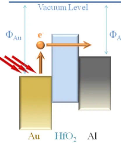
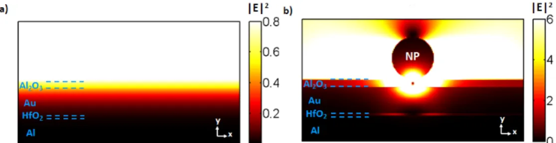
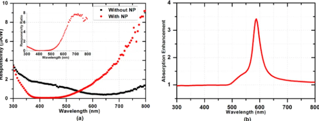
Plasmonically enhanced hot electron based photovoltaic device
Tam metin
Şekil
Benzer Belgeler
To this end, we aim to measure explanatory and forecast power of consumer confidence indices on future private consumption growth through three questions: (i) “Does consumer
Therefore, the present special issue has been put together to review and highlight the recent work of some prominent scientists around the world dealing with the “charging”.. We
challenges the views of adherents of the doctrine of raison d'?tat who give rulers the license to disobey legal and moral norms whenever the vital interests of the state are
Sınır testi ve ARDL yaklaşımlarının kullanıldığı ampirik analizlerden elde edilen sonuçlar Türkiye'nin savunma harcamalarının dış borç değişkeni üzerinde
V, we consider the regular-discrete time scales and introduce the algebra of shift operators on them and give the corresponding GD formulation for all such time scales.. Here
The existence of the inverses of the Hamiltonian operators (7) and (12) is sufficient to establish their non-degeneracy so that the conditions of Magri’s theorem are
Basically, stress due to displacement of the cantilever changes the local refractive index on the ring resonator through the photo-elastic effect , and index change
The parallel strategy requires the allocation of an available budget to a number of R&D activities, the determination of the number of research teams within each activity and
