PROCEEDINGS OF SPIE
SPIEDigitalLibrary.org/conference-proceedings-of-spieHigh-speed GaAs-based
resonant-cavity-enhanced 1.3-um
photodetector
Ekmel Ozbay, Ibrahim Kimukin, Necmi Biyikli, Gary
Tuttle
Ekmel Ozbay, Ibrahim Kimukin, Necmi Biyikli, Gary Tuttle, "High-speed
GaAs-based resonant-cavity-enhanced 1.3-um photodetector," Proc. SPIE
3948, Photodetectors: Materials and Devices V, (13 April 2000); doi:
10.1117/12.382116
Event: Symposium on Integrated Optoelectronics, 2000, San Jose, CA,
United States
High-Speed GaAs Based Resonant Cavity Enhanced 1.3 Micron
Photodetector
Ekmel Ozbaya, Ibrahim Kimukina, Necmi Blyikila and Gary Tuttleb
aDepartment of Physics, Bilkent University,
Bilkent, Ankara, 06533 TURKEY
bMicroelectronics Research Center, Iowa State University,
Ames, IA 50011
ABSTRACT
High-speed photodetectors operating at 1.3 and 1.55 im are important for long distance fiber optic based telecom-munication applications. We fabricated GaAs based photodetectors operating at 1.3 ,urri that depend on internal
photoemission as the absorption mechanism. Detectors using internal photoemission have usually very low quantum
efficiency. We increased the quantum efficiency using resonant cavity enhancement effect. Resonant cavity
en-hancement effect also introduced wavelength selectivity which is very important for wavelength division multiplexing based communication systems. The top-illuminated Schottky photodiodes were fabricated by a microwave-compatible
monolithic microfabrication process. The top metal layer serves as the top mirror of the Fabry-Perot cavity. Bot-tom mirror is composed of 15 pair AlAs/GaAs distributed Bragg reflector. We have used transfer matrix method to simulate the optical properties of the photodiodes. Our room temperature quantum efficiency measurement and
simulation of our photodiodes at zero bias show that, we have achieved 9 fold enhancement in the quantum efficiency, with respect to a similar photodetector without a cavity. We also investigated the effect of reverse bias on quantum efficiency. Our devices are RC time constant limited with a predicted 3-dB bandwidth of 70 GHz.
Keywords: Photodetector, Internal-photoemission, RCE Effect, Infrared, Fiber Communication
1. INTRODUCTION
There is an increasing demand for larger telecommunication bandwidth, as the information revolution continues at an increasing pace. The optical communication systems are currently the only viable solution for this bandwidth demand. Optical components such as semiconductor lasers, photodetectors, modulators, and optical amplifiers are
the hearth of these communication system, and the performance of all these components should be increased to meet
the existing and expected bandwidth requirements. Besides the optical communication systems, high-performance photodetectors are also vital components of optical measurement systems. Both p-i-n and Schottky photodiodes'
offer high-speed performance to fulfill the needs of such systems. Resonant cavity enhanced (RCE) photodetectors offer the possibility of overcoming this limitation in the bandwidth-efficiency product of conventional photodetectors.2
2. THEORY
2.1. Internal Photoemission
With the advent of silicon and gallium arsenide molecular beam epitaxy growth technique, novel SiGe/Si, GaAs and
Si homojunction detectors have been demonstrated in addition to the IrSi Schottky contact internal photoemission detectors for the operation in the infrared and far infrared region.36 These detectors, which are fabricated by
standard Si or GaAs integrated circuit processing procedures, are among the most promising sensors for large-scale monolithic infrared imaging arrays.
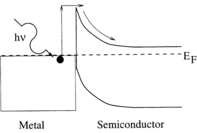
Internal photoemission corresponds to the optical excitation of electrons in the metal to an energy above the
Schottky barrier and then transport to the conduction band of the semiconductor which is shown in Fig. 1 .According
to the theory developed by Fowler, the number of electrons emitted per quantum of light absorbed is to a first approximation proportional to the number of electrons per unit volume of the metal whose kinetic energy normal to the surface is sufficient to overcome the potential step of the surface.7 We may call this number the number of
available electrons.
Metal
Semiconductor
Figure 1. Excitation of an electron in the internal photoemission process.
In a gas of electrons obeying the Fermi-Dirac statistics, the number of electrons per unit volume having velocity
component in the range u + du, v + dv, w + dw is given by the formula:
(\
dudvdwn(uvw)dudvdw=2(—}
\
(1)h
I
e[m(u2+v2+w2)_EF1/kT+ 1The number of electrons per unit volume n(u)dn with velocity component normal to the surface in the range u,
U + du is given by:
m [271 pdpd9 n(u)du =2
()
duJ
e[m(u2+p2)_EF1/kT + 1 (2)when the integral is taken, we end up with an expression::
n(u)du =4rrkT
()3
log[eEF_mu2/kT+ 1]du (3)As explained before, only the electrons with a total kinetic energy (after absorbing the photon with energy hv)normal
to the interface is larger than EF + B can go over the Schottky barrier and contribute to the photocurrent. The
number of available electrons is given by:
N=f
n(u)du (4)mu2=EJ+ØB hv
where n(u)du is given by Eq.(2.20). By making a change of variable y = (hv—cB —EF
+ mu2)/kT ,
weobtain:N
——2rkT
1rn3
[°° log[1 + e_(
B)/hT] d 5m
m )
h)
J
[y+ (EF + B —hv)/kT]To simplify this integral, we consider the region hv near cbB.Then,it is a good approximation to neglect y in the
denominator of the integral, hence we obtain,
2 3/21kT2
'°°
N = v
irm1/2
J log[1
+ e_T] dy
(6)(a) When y = (hi'—qB)/kT< 0, the logarithmic term can be expanded, and integrated term by term. Then
2\/ irm312 (kT)2
e e3'
1N=
h3
E2
e ---+--—j
(7O)
(7)Absorption
Region
,z=o
v _______ Z=L
I. III
E1 aex aex —0—øEf
Eb-*
LI
Incident
Light
-t1
I I•
. III
DBR 1d
L2 :&/4 WaveDBR Reflector
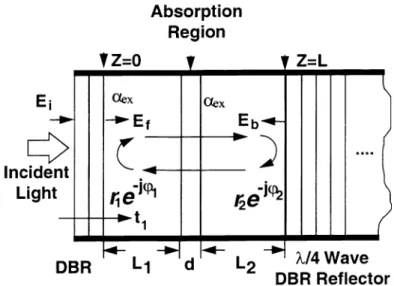
Figure2. Analysis model of an RCE photodetector.
(b) When y =(hu—q1B)/kT 0, the logarithmic term can be expanded, and integrated term by term, giving
00
2 1
e2
L
log[1+
dy =+ 2
_ 22 32 • • ] (8)2/ irm32 (kT)2 2
2 1 — e2
e3
\
N=
h3E'2
-e —----+----—)
(y>O) (9)We are interested in the situation 'y >0. Above threshold, for 'y >6our expression takes the form
N=AT272
(10)with an accuracy of 5%•8 We can assume that the photoelectric current I per quantum of light absorbed is
proportional to N. Sofor internal quantum efficiency, we can write:
I
(hv—5B)2 , (hu >B)
11l
0 ,(hv<B)
( )Eq. 11 is derived for bulk material, and the thickness of the Schottky layer isn't taken into account. When the
reflections from the walls of the metal are taken into account, it has been found that there is an enhancement in the quantum efficiency, but the dependence on the wavelength of the photons is the same.911
2.2. Resonant Cavity Enhancement
For transit time limited photodetectors, the depletion region must be kept thin for the high speed operation. On the other hand, for high quantum efficiency the depletion layer must be sufficiently thick to absorb a high fraction
of incident light. To overcome this trade off between the response speed and efficiency, we can place a conventional
photodetector with a thinner active layer inside a Fabry-Perot microcavity. Thinner active layer results in lower transit time, which increases the performance of the photodetector. This kind of enhancement of the quantum
efficiency is called resonant cavity enhancement (RCE) .RCEeffect was proposed in 1990 and was applied to a broad range of detectors : 2, 1 3 pj,141 6 and 8 photodiodes.
Fig. 2 shows a generalized structure of an RCE photodetector. As the aim is to achieve maximum efficiency,
lossless distributed Bragg reflectors (DBR) are used as mirrors of the microcavity. Active layer, where the absorption
occurs, is placed between these mirrors. L is the length of the cavity and d is the thickness of the active layer. The
to the light penetration into the mirrors. E represents the electric field amplitude of the incident light, while E1 is the forward traveling wave at z = 0,and Eb is the backward traveling wave at z = L. In the cavity, Ef is composed
of the transmitted wave from the first mirrors and the reflected wave from the second mirror. Therefore the forward
traveling wave, Ef, at z =0can be obtained in a self-consistent way:
E1 =
t1E
+ rlr2e__(L1+L2)e2(212)Ef
(12) where 3 =271n/Ao, and c are the absorption coefficients of the active and cavity layers respectively. Solving forEf gives us
E
I —_
tl
E 13andbackward traveling wave, Eb, at z =Lcan be expressed as,
Eb r2e_e1+L2)e_i2)Ef.
(14)The optical power inside the resonant cavity is proportional to the refractive index of the medium and the square of
the electric field amplitude.
P(z) cx E(z)2n (15)
where E(z) =E1(z)+ Eb(z) is the total electric field. Neglecting the standing wave effect, the power absorbed in
the active layer is given by:
1 2 —cxL1 2 —cL2—cL —ad
P1 =
_
2r1re
cos(2flL± i + 2) + (rir)2e2
(16)where cx =(0ex(L1 + L2) + cd)/L. Under the assumption that all the photogenerated carriers contribute to the
current, ij is the ratio of the absorbed power to the incident optical power. i.e., r =P1/Pt. Hence:
(
e_L1 +R2e2ez')
—ad—
1—
2R2ecL
cos(2fiL + i 02) + R1R2e
(1 —R1)(1—e
) (17)
While designing the detector, the cavity layers are chosen such that all the light is absorbed in the active layer
(cex << a) . The expression in the square braces is call the enhancement, as it is the multiplier to the quantum
efficiency of a conventional photodiode. Enhancement can be rewritten as:
(1 D ad
1
-1-- it2eenhancement = (18)
1 —2R1R2
e°" cos(23L + q5i + 2) + R1R2 ed
From this expression, it is seen that i is enhanced periodically at the resonant wavelengths of the cavity,
2/3L + &
+
2 2mir (m =
1,2, 3...). This term introduces the wavelength selectivity of the RCE effect.3. DESIGN
The external quantum efficiency (QE) can be found by multiplying the absorption in the Schottky layer and the
internal quantum efficiency. The thickness of the Schottky layer should be kept small to get a higher internal quantum
efficiency, on the other hand, the absorption decreases as the thickness gets smaller. We can get over this trade-off by placing the Schottky layer inside of a Fabry-Perot cavity.
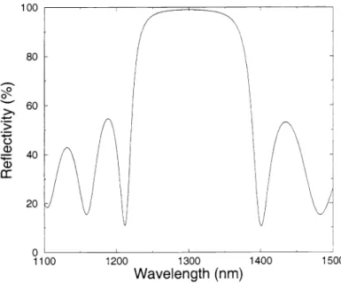
Our detectors consist of GaAs layers as cavity layers, N- layer is very lightly doped, and N+ region is doped to 1018 cm3 for the ohmic contact. Bottom mirror consists of 15 pair AlAs/GaAs DBR centered at 1.3 tim. This mirror has reflectivity greater than 95% between 1244 nm and 1359 nm. Maximum reflectivity of 99% is achieved at l300nm. Fig. 3 shows our reflectivity simulation of the bottom mirror calculated using transfer matrix method
(TMM).
Before the process, comparing the measurement and the simulation of the reflectivity, we realized that there was a %4 deviation of thickness from our design. Fig. 4 shows the measured reflectivity and our simulation fitted to this
data. By etching the top GaAs layer, the resonance frequency is tuned to 1.3 tim.
100 80
60
>
0
40
Q) 20 0 1100Figure 3. Reflectivity simulation of the bottom mirror.
80 60
>
>
0
- 40
20 1200 1300 1400 Wavelength(nm) 1500 100 1300 0 1250 1350 1400 1450 1500 Wavelength (nm)Ohmic Metal Air Bridge Si1N4
__________
ITO layer Au Schottkv layer Interconnect Metal>
0 C a)0
w E Ca0
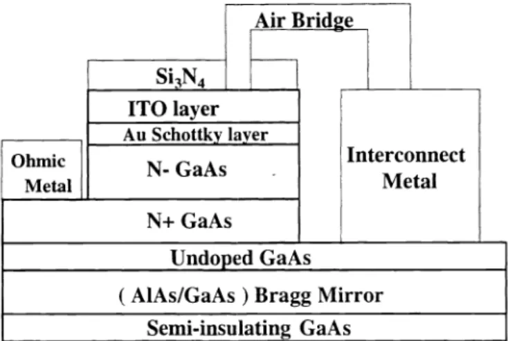
Figure 5. Cross-section of a fabricated device. N- GaAs
N+ GaAs
Undoped GaAs
7
(AlAs/GaAs
)
BraggMirror
Semi-insulating GaAs 1200 1300 1400 Wavelength(nm) 0.08 0.06 0.04 0.02 0 1100 1500
Figure 6. Measured (solid line) and simulated (dotted line) quantum efficiency as a function of wavelength.
4. FABRICATION
The top-illuminated Schottky photodiodes were fabricated by a microwave-compatible monolithic microfabrication
process. Fig. 5 shows the schematics of the fabricated devices. Fabrication started with formation of ohmic contact to N+ layer. Mesa isolation was followed by a Ti-Au interconnect metallization. A 6 nm Au-Schottky layer, a 100
nm transparent-conductor indium tin oxide (ITO) layer, and silicon nitride were deposited. The thickness of the ITO and silicon nitride layer was chosen to form an antireflection coating at 1.3 pm. Finally, a thick Ti-Au was deposited
to form an air-bridge connection between the interconnect and the ITO layer. In this structure, the top gold layer serves as both the top mirror of the Fabry-Perot cavity and the absorbing layer.
Cl) C
>
-ow
0
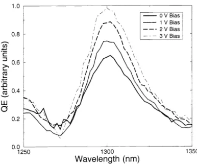
1300 Wavelength (nm) 1350Figure 7. Quantum efficiency under various reverse biases.
0.008 0.006
>
Q) 0.0040
>
0.002 0.000 0 1000Figure 8. Response of a 1O0m2 area device under zero bias.
200 400 600 800
5. MEASUREMENTS
Photospectral measurements were carried out by using a tungsten-halogen light source and a monochromator. This
light is chopped and coupled to a 62.5 m diameter multimode fiber. Chopped light is delivered to the 150 x 15Oim2
areadevice by a lightwave fiber probe, and electrical contacts are made on the probe station. In Fig. 6, we present the room temperature QE measurement and simulation of our photodiodes at zero bias. Our simulations show that, we have achieved 9 fold enhancement in the QE, with respect to a similar photodetector without a cavity.
We also investigated the effect of reverse bias on QE. Fig. 7 shows the QE of a photodiode under various reverse
bias voltages. Applying reverse bias decreases the barrier height, which in turn results in a higher QE.
High speed measurements were made at 765 nm. 1 psec full width half max (FWHM) laser pulses were generated at 1530 nm and these pulses were used to generate 765 nm pulses using second harmonic generation. Optical pulses
were coupled to a single-mode fiber, and the pulses frOm the fiber were coupled to the devices. Fig. 8 shows the response of a 100 m2 area device measured with a 50 GHz sampling scope. Measured FWHM of the response was 20 psec. The deconvolved 3-dB bandwidth of the detector is 20 GHz. The unexpected tail in the response of the detector is due to the diffusion of the carriers generated in the N+ layer. Since there is no absorption in the cavity layer at 1.3 pm, we hope to get our expected high-speed response with a pulsed source at 1.3 pm.
6. CONCLUSION
In summary, we reported our efforts in fabrication and charcterization of GaAs based internal photoemission detectors operating at 1.3 pm. We hope to improve the high-speed performance of our devices using a pulsed source operating
at 1.3 pm, where we don't suffer from absorption in the cavity layers.
ACKNOWLED GMENTS
This work is supported by NATO Grant No.SfP97197O.
REFERENCES
1. K. D. Li, A. S. Hou, E. Ozbay, B. A. Auld, and D. M. Bloom, "2-picosecond, GaAs photodiode optoelectronic circuit for optical correlation applications," Appi. Phys. Lett. 61, p. 3104, 1992.
2. M. S. Unlü and S. Strite, "Resonant cavity enhanced photonic devices," J. Appi. Phys. 78, p. 607, 1995. 3. J. S. Park, T. L. Lin, E. W. Jones, H. M. D. Castillo, and S. D. Gunapala, "Long-wavelength stacked SiGe/Si
heterojunction internal photoemission infrared detectors using multiple SiGe/Si layers," Appi. Phys. Lett. 64,
p. 2370, 1994.
4. W. Z. Shen, A. G. U. Perera, H. C. Liu, M. Buchanan, and W. J. Shaff, "Bias effects in high performance GaAs
homojunction far-infrared detectors," Appi. Phys. Lett. 71, p. 2677, 1997.
5. A. G. U. Perera, W. Z. Shen, H. C. Liu, M. Buchanan, M. 0. Tanner, and K. L. Wang, "Demonstration of Si homojunction far-infrared detectors," Appi. Phys. Lett. 72, p. 2307, 1998.
6. B.-Y. Tsaur, M. M. Weeks, R. Thbiano, P. W. Pellegrini, and T.-R. Yew, "IrSi Schottky-barrier infrared detectors with 10-pm curoff wavelength," IEEE Elect. Dev. Lett. 9, p. 650, 1988.
7. R. H. Fowler, "The analysis of photoelectrical sensitivity curves for clean metals at various temperatures," Phys. Rev. 38, p. 45, 1931.
8. G. Gigli, M. Lomascolo, M. D. Vittorio, R. Cingolani, A. Cola, F. Quaranta, L. Sorba, B. Mueller, and A. Fran-ciosi, "Direct assesment of tunable schottky barriers by internal photoemission spectroscopy," Appi. Phys. Lett. 73, p. 259, 1998.
9. V. E. Vickers, "Model of Schottky barrier hot-electron-mode photodetection," Appi. Opt. 10, p. 2190, 1971.
10. V. L. Dalal, "Simple model for internal photoemission," J. of Appi. Phys. 42, p. 2274, 1971.
11. E. Y. Chan, H. C. Card, and M. C. Teich, "Internal photoemission mechanisms at interfaces between germanium
andthin metal films," IEEE J. of Quantum Electron. 16, p. 373, 1980.
12. E. Ozbay, M. S. Islam, B. Onat, M. Gökkavas, 0. Aytür, G. Tuttle, E. Towe, R. H. Herderson, and M. S. Unlü, "Fabrication of high-speed resonant cavity enhanced schottky photodiodes," IEEE Photon. Technol. Lett. 9,
p. 972, 1997.
L661 '191 •d
'oi
•7
uod1osqi
pu
Uo3JdJnm
spoTpooqdoi
ZHDqMpuiq-uii
'3npo1d 7ddyoiods
'a
y
'"i-'v
i'H
s
s
'zsnj,
o
'uui
pu
ç'Joqdur3
poods-qi,,
II