Hybrid Stacked Memory Architecture for Energy
Efficient Embedded Chip-Multiprocessors Based on
Compiler Directed Approach
tSalman Onsori, tArghavan Asad
tComputer Engineering Department tBilkent University
Ankara, Turkey
[email protected], ar _ [email protected] Abstract-Energy consumption becomes the most critical limitation on the performance of nowadays embedded system designs. On-chip memories due to major contribution in overall system energy consumption are always significant issue for embedded systems. Using conventional memory technologies in future designs in nano-scale era causes a drastic increase in leakage power consumption and temperature-related problems. Emerging non-volatile memory (NVM) technologies are promising replacement for conventional memory structure in embedded systems due to its attractive characteristics such as near-zero leakage power, high density and non-volatility. Recent advantages of NVM technologies can significantly mitigate the issue of memory leakage power. However, they introduce new challenges such as limited write endurance and high write energy consumption which restrict them for adoption in modern memory systems. In this article, we propose a stacked hybrid memory system to minimize energy consumption for 3D embedded chip multiprocessors (eCMP). For reaching this target, we present a convex optimization-based model to distribute data blocks between SRAM and NVM banks based on data access pattern derived by compiler. Our compiler-assisted hybrid memory architecture can achieve up to 51.28 times improvement in lifetime. In addition, experimental results show that our proposed method reduce energy consumption by 56% on average compared to the traditional memory design where single technology is used.
Keywords-Hybrid memory architecture; Non-Volatile Memory (NVM); embedded Chip-Multiprocessor (eCMP); con vex
optimization based model, Compiler-assisted
I. INTRODUCTION
Chip-multiprocessor (CMP) architectures have been extensively adopted to meet ever-increasing demands on performance in embedded systems. The increase in the number of cores in embedded CMPs comes with an increase in energy consumption. Energy consumption is an essential and important constraint for embedded systems since these systems are generally limited by battery lifetime. In addition, significant amount of embedded system's power consumption is due to memory system. Therefore, there is a critical need to reduce energy consumption of memory architecture in embedded systems.
In order to reduce memory energy, it is needed to address both the leakage and dynamic energy. On the other hand, 42% of overall energy dissipation in the 90nm generation is consumed by leakage energy [1] and this value can exceed above 50% in 65nm technology [2]. Hence, leakage energy has
tOzcan Ozturk, tMahmood Fathy
tComputer Engineering Department ,'Iran University of Science and Technology
Tehran, Iran
[email protected], [email protected]
become comparable to dynamic energy in current generation memory modules and soon exceed dynamic energy in magnitude if voltage and technology are scaled down any further [3]. Consequently, architecting energy efficient memory hierarchy with the lowest leakage energy is especially critical for embedded systems.
In this article, to overcome physical limitation of two dimensional integration, three dimensional integrated circuit(lC) is exploited. 3D integration technology reduces power of on-chip communication while it increases on-chip communication bandwidth. Furthermore, we can build heterogeneous CMP utilizing 3D integration technology.
A number of researchers proposed 3D CMP architectures with 3D stacked memory system [4, 5]. Stacking main memory directly on top of a core layer is a natural way to attack the memory wall problem. Stacked traditional memories such as SRAM and DRAM on the core layer may cause a drastic increase in perfonnance degradation, power density and temperature-related problems.
Various Non-volatile memories such as Spin-Torque Transfer RAM (STT-RAM), Phase-Change RAM (PCRAM) and Resistive RAM (ReRAM) have been emerged as promising candidates for next generation computing system. NVMs are potentially attractive to design new classes of memory systems as an alternative of traditional memories due to their benefits such as higher storage density and near zero leakage power consumption. STT-RAM as a promising candidate of NVM technologies combines the speed of SRAM, the density of DRAM and the non-volatility of Flash memory. In addition, excellent scalability and very high integration with conventional CMOS logic are the other superior characteristics of STT-RAM [4]. Although STT-RAM and other NVM memory technologies have many advantages, drawbacks such as high write energy consumption, long latency writes and limited write endurance prevent them from being directly used as a replacement for traditional memories in embedded systems.
In order to overcome the mentioned disadvantages of 3D stacked traditional memory architectures, and due to drawbacks of NVM memories to be directly used as a replacement for traditional memories, we need to exploit SRAM and STT-RAM as two different type of memory banks in the stacked memory layer. This hybrid memory architecture leads us to the best design possibility with using advantages of both memory technologies.
Since allocating data blocks to different memory technologies have considerable impact on energy consumption due to different features of SRAM and NVM, we should make a decision for these allocations in order to design an energy efficient hybrid memory architecture. As we mentioned earlier, NVM technologies have two main shortcomings caused by write activities. They have long write latency and dynamic energy compared to traditional memory technologies such as SRAM. On the other side, NVM has near zero leakage power as a promising feature in nowadays nano-scale designs. In order to overcome the mentioned disadvantages of NVM technologies, different approaches focused on designing hybrid memory system at both circuit and architecture levels.
To achieve efficient allocation for distributing data blocks into different memory technologies in a hybrid architecture, we exploit compiler to collect information of read and write accesses from application code in this work. Compiler assists us for doing these analyses with providing information about data access pattern. By utilizing compiler analysis to design a hybrid memory architecture,
it
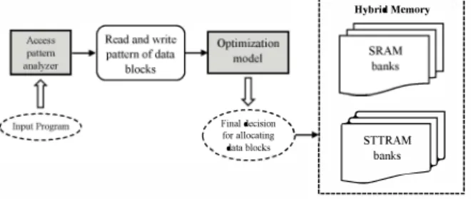
is possible to prevent remarkable extra hardware overheads required by runtime solutions. Specifically, it frees the architecture from expensive dynamic checking. Consequently, efficient allocation of data blocks into NVM and SRAM memory banks for architecting a hybrid memory system is tightly coupled with the compiler. With exploiting compiler, we can take full advantages of NVM and SRAM memory banks by enforcing data blocks to be allocated to specific memory type. In this work, we obtain data access patterns by using compiler and analyze their read and write information in order to efficiently allocate data blocks to SRAM or STT-RAM banks. System optimization techniques are widely used to improve overall performance as well as energy efficiency. In this work, we propose a convex optimization based approach to design a heterogeneous memory system consists of NVM and SRAM memory banks. To the best of our knowledge, this is the first time that a convex model is used for architecting an optimal hybrid memory system using compiler. Our proposed model minimizes energy consumption of the embedded 3D CMP with respect to the performance. Figure 1 shows an overview of the proposed approach.n
Hybrid Memory�
�
";F:l:1-d:C�S;O:1""\
[3TTRAM
t for allocatmg r---+l"
, 'I banks
data blocks ,' I1 ___________________________ _
Fig. 1. Overview of the proposed method.
The main contributions of this work can be summarized as follows:
• To the best of our knowledge this is the first work that proposes optimization model to distribute data blocks into SRAM and STT-RAM banks based on compiler analysis.
• We efficiently allocate data blocks based on read and write access patterns.
• We minimize energy consumption of stacked hybrid
memory onto eCMP by utilizing compiler for the first time.
The remainder of this paper is organized as follows. Section II describes related works. In Section III, the details of convex optimization-based problem and its formulation are investigated. In Section IV, evaluation results are presented. Finally, we draw conclusions at Section V.
II. RELATED WORK
Recent studies [6][7][17][18][19][20] have proposed hybrid architectures, wherein the SRAM is integrated with NVMs to use advantages of both technologies. Energy consumption is still a primary concern in embedded systems since they are limited by battery constraint. Several techniques have been proposed to reduce energy consumption of hybrid memory architectures in embedded systems. Fu et al. [9] presented a technique to improve energy efficiency through a sleep-aware variable partitioning algorithm for reducing the high leakage power of hybrid memories. Hajimiri et al. [8] proposed a system-level design approach that minimizes dynamic energy of a NVM based memory through content aware encoding for embedded systems. Our work is different from all these prior works as we focus on allocation of data blocks to SRAM and STT-RAM banks in memory of embedded system based on data access pattern to minimize energy consumption with using an optimization model.
There are several works that exploit compiler approaches to design memory systems. Wang et al. [10] proposed a new block placement and migration policy for a hybrid last level cache that places data based on access patterns. They analyze the access pattern of each write access type, and suggest a block placement policy that adapts to the access pattern for each class. Li et a!. [11] proposed an all-STT-RAM cache hierarchy. They propose a compiler technique that analyze cache read/write accesses and configure memory cells into the appropriate mode to accelerate data reads. Authors in [12] described methodologies that leverage compiler analyses which expose data access and communication patterns within the multi-threaded applications and use this information to efficiently configure hardware that uses STT-RAM. Chen et al. [13] proposed a technique for initial placement of data blocks in hybrid memory by the compiler hints while the dynamic migration is designed with hardware mechanisms. Algorithms for determining ratio of SRAMINVM and allocation of data into SRAM and NVM at compile time is presented in [14]. Ozturk et al. [15] minimized energy of banked memories based on data access pattern information extracted by compiler. However, we propose a compilation-based approach to improve the energy-efficiency and performance of 3D stacked hybrid memory architecture in future CMPs based on a convex optimization model.
III. PROPOSED METHODE
A. Data Access Pattern Extraction and Analysis
As illustrated in Figure 1, the first step of our approach is to extract data-access pattern information from the application code. While it is possible to do this by profiling the code under consideration, the resulting access pattern may be very sensitive
to the particular input used in profiling. Instead, in this work, we use static compiler analysis to extract read and write information of data-access patterns of given embedded application. Then, we use this read and write access pattern for allocating data blocks to the appropriate memory bank. In this work, we force write intensive blocks to be allocated in SRAM banks due to its higher endurance and lower energy consumption for write operations. With this policy, we can assign STT-RAM banks for read intensive blocks to take advantage of near zero leakage power of NVM technology and more reliable design with preventing write operations in STT-RAM banks.
A sample data-access pattern is shown in Figure 2(a). In this figure, we also represent type of accesses (read and write) to each data block. For example,
ar
represents read access andaw
represents write access to data blocka
in the sample data pattern. Figure 2(b) shows number of write and read accesses to data blocks of the sample data-access pattern. The following paragraphs discuss the details of our compiler-directed access pattern analyzer.(a)
j
[gJ
Write activity: I. Read activity 4[IJ
Write activity 2, Read activity: IW
Write activity: 3, Read activity 2 (b)Fig. 2. (a) A sample for a data-access pattern ; (b) Read and write activity of data blocks a, b, c in the data-access pattern.
Embedded programs constructed using loop nests (with compile time known bounds) and array accesses (with affine subscript expressions) are the main focus in this article. Such codes frequently occur in the embedded image/video processing domain. An optimizing compiler can analyze these loop intensive applications with regular data-access patterns. Since write intensive data blocks are a short percentage of data blocks, an early design decision we made is to allocate write intensive blocks into SRAM banks. In our implementation, write and read activities of blocks are expressed in terms of loop iterations. Specifically, in this work, we approved the concept of a step to define these transitional intensive blocks. Even though, in theory, we have the flexibility to assign any number of iterations between two transitional events, these points should be selected carefully. In other words, in moving from one step to another during execution, the data-access pattern should exhibit significant variation.
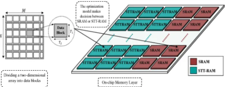
The unit of data that is being stored in SRAM or STT-RAM banks in our experiments is a data block. The data-block size is a crucial factor which affect data-access pattern. We manually selected suitable data-block sizes for a given application. Figure 3 shows a general view of allocating a data block to on-chip memory layer. In this figure, a two-dimensional array is divided into data blocks at the left part. Data blocks can be allocated to SRAM or STT-RAM banks by result of optimization model.
'�-��-.---�---', : D1Vldmga two-dnllcnsional: : array into data blocks :
',---,
Fig. 3. Dividing a two-dimensional array into data blocks and mapping a data block into a SRAM or STT-RAM bank in hybrid on-chip memory layer based on solving the optimization problem at compilation time.
The left side of Figure 4 is an example of loop nest that accesses an array X and Y through two references with affine subscript expressions X
[i,j]
and YU, i].
Blocked version of the original loop nest is given on the right-hand side of the same figure. In this code, loopsk
andl
iterate over the data blocks and loops m and n, on the other hand, iterate over the elements of agiven data block.
fori=l,N,l forj=l.M.l ==> X[i,j] = YU,ij + 2 fork=l,N,T, for 1 = 1 , M , Tz for m=k,min(N,k+T,-1),1 for n=l,min(M,I+Tz-l),l X[m.nj = Y[n,mj + 2
Fig. 4. An example of loop nest written in a pseudo code (left) and its blocked (or tiled) version (right). Each data block (tile) is of size Tl x T2 array elements, and the transformed loop nest is structured based on this tile size.
Figure 5(a) shows two two-dimensional arrays of the same size divided into data blocks. Note that there are write accesses to array X and read accesses to array Y. Now, the pseudo code shown in Figure 5(b) accesses the data blocks
a, e,f, g, h,
andb,
under the data block partitioning given in Figure 5(a). Specifically, when this loop nest is executed, read and write data access pattern of the blocks isaw, en in gn hn bw'
Assuming that the entire code fragment is considered as a single execution step, these are also the blocks accessed in this step. However, if we assume that each step consists of onlyQ2 /4
loop iterations, then the iteration space of the code fragment shown in Figure 5(b) spans two steps, In this case, the data blocks accesses by the first step areaw, en in gn
andhr;
and those accessed by the second step arebw , er, ir, gr,
andhr.
These two sequences collectively constitute thedata-block access pattern
for this code fragment. Consequently, dividing loop nest into steps can change access pattern sequence of our application.x Block a Block b Block c Block d ( ) Q y Block e Block f Block g Block h for i = 1, Q/2 for j = 1, Q X[i,j] = Y[j, i] + 2 I:?
Fig. 5. Two two-dimensional arrays (X and Y) divided into four blocks each; (b) example code fragment operating on these arrays.
TABLE!. THE CONSTANT TERMS USED IN OUR CONVEX Constant Definition
P N umber of cores in the core layer N N umber of SRAM memory banks M Number ofSTT-RAM memory banks B N umber of data blocks
S Number of steps sizehlock Size of a data block
sizeSRAM Available SRAM memory space size<TTRAM Available STT-RAM memory space
ERsRAM Average Energy consumed by a read accessed from the SRAM memory bank per step EWSRAM Average Energy consumed by a write accessed to the SRAM memory bank per step ERsTTRAM Average Energy consumed by a read accessed from the STT-RAM memory bank per step EWSTTRAM Average Energy consumed by a write accessed to the STT-RAM memory bank per step
PSSRAM Static power consumed by an SRAM memory bank per step PSSTTRAM Static power consumed by an STT-RAM memory bank per step
r Step size
r
f
RAM SRAM bank Average time to read a data block from the rfR
AM SRAM bank Average time to write a data block to the rf
TTRAM STT-RAM bank Average time to read a data block from the rfT
TRAM Average time to write a data block to the STT-RAM bankB.
Problem Formulation
In this section, we propose a convex optimization model which targets optimization of a linear objective function subject to linear constraints and integer solution variables. The outputs of our optimization problem are:
1. The optimal placement of data blocks into SRAM and STT-RAM banks based on their read/write access behavior.
2. Minimization of energy consumption of the proposed 3D stacked memory with respect to the performance constraint.
To solve the models, we use CVX [16], an efficient convex optimization solver. Assuming that
P
denotes the total number of cores, N the total number of SRAM memory banks, M the total number of STT-RAM memory banks, B the total number of data blocks and S the total number of steps.We use Rm,s and Wm,s to identify if there is a read or write access to a data block in one step. More specifically:
• Rm,s: Indicates whether data block m is read accessed
at step s.
• Wm,s: Indicates whether data block m is write accessed
at step s.
Assignment of a data block to a memory bank is identified by LSRm,n and LSTm,n' That is,
• LSRm,n: Indicates whether data block m is assigned to
SRAM bank n.
• LST m,n : Indicates whether data block m is assigned to
STT-RAM bank n.
Read or write access to a memory bank with a data block at a particular step is captured by SRn,m and STn,m' Specifically, we have:
• SRn,m: Indicates whether SRAM bank n is accessed by
data block m.
• STn,m: Indicates whether STT-RAM bank n is accessed
by data block m.
After having defmed integer variables, we can now discuss our model formulations. The following constraints are needed to capture the values of SRn,m and STn,m' More specifically, STn,m equals to one if data block m is in STT-RAM bank n and data
block m is read or written in this bank. Similarly, SRn,m equals
to one if data block m is in SRAM bank n and data block m is
read or written in this bank. Access constraints are shown in equation 1 through 4. As follow:
SRn,m ;::: Rm,s
xLSRm,n'
Vm, n, S(1)
STn,m ;::: Rm,s
xLST m,n'
Vm, n, S(2)
SRn,m ;::: Wm,s
xLSRm,n'
Vm, n, S(3)
STn,m ;::: Wm,s
xLST m,n'
Vm, n, S(4)
Since a data block can reside only in a single bank at any given time, it must satisfy the following constraint.N M
L
LSRm,i
+L
LST m,j
=1,
Vmi=1
j=1
(7)
The limited bank capacity establishes the basis for the next constraint that needs to be included in our model. Assuming that the size of a block is sizeblock and the available memory space is sizeSRAM and sizeSTTRAM for SRAM and STT-RAM memory space, respectively. Hence, each memory bank will be of size
sizeSRAM for SRAM and sizeSTTRAM for STT-RAM.
N M B
.
'\'
sizeSRAM SLzeblock xL
i=1
LSRi,n
:5 N ' B.
'\'
sizeSTTRAM SLzeblock xL
i=1
LSTi,n
:5 M ' Vn(8)
Vn(9)
If number of writes for a data block is more than a threshold number, we force the data block to be allocated in SRAM bank. We employ following constraint for this target:
LSRm,n x
(I
Wm,j)
+ LSTm,n x thresholdwrite 2: thresholdwrite,}=1
To force a data block to be allocated in SRAM, we also need to prevent allocation of the data block to STT-RAM simultaneously. Hence, constraint (11) allows allocation of the data block to STT-RAM bank only when number of writes are less than the threshold:
LSTm,n x
(t
Wm,j)
:5 thresholdwrite.'tm.q.m"* q.'tn
(11)
So far in our discussion we have not put any limit on the potential performance degradation due to using SRAM or STT RAM memory banks for allocating data blocks, One might envision a case where only a limited degradation
in
performance could be tolerated, The performance overhead in our model can be captured using an additional constraint In our design, the performance overhead is mainly due to different delay of write Iread activities in SRAM and STT-RAM banks. Assuming that Omax is the maximum performance overhead allowed for the design (which can be 0 to obtain the best energy savings without tolerating any performance penalty), then our performance constraint can be expressed as follows:S
8 N 0=I I (I
(SRk,m
XRm,s
xrfRAM
+SRk,m
XWm,s
Xr�AM)
s=1 m=1 k=1
M
+I
(STk,m
XRm,s
xrfTTRAM
+Sh,m
xWm,s
k=1
xrfrTRAM))
:5 Oma
x(12)
We define the dynamic energy consumption as the sum of read and write energies of data blocks in SRAM or STT-RAM banks.
S
8 NEdynamic
=I I (I
(SRk,m
XRm,s
xERsRAM
+SRk,m
XWm,s
s=1 m=1 k=1
XE WSRAM)
M
+I
(Sh,m
xRm,s
xERsTTRAM
+STk,j
XWm,s
k=1
xE WSTTRAM))
(13)
In addition, we calculate static energy, The static power dissipation depends on temperature, Since this optimization approach is solved at design time, we consider pessimistic worst-case temperature assumption and calculate
Pstaticsr
andPstaticst
at maximum temperature limit Specifically, that is:S
NS M
Estatic
=I I
r
xPSRAM
+I I
r
xPSTTRAM
s=1 k=1
s=1 k=1
(14)
Having specified the necessary constraints in our convex optimization model, we next propose our objective function, We denote the total energy consumption of the proposed 3D-stacked heterogeneous memory system as
ETotal, ETotal
is comprised of dynamic and statics power components:minimize
ETotal
=Edynamic
+Estatic
(15)
To summarize, objective function ETotal is minimized under constraints (1) trough (14), This proposed memory system is very flexible and we can use other types of NVM banks in ourarchitecture, For example, we can use PCM instead of STT RAM and DRAM instead of SRAM in the memory layer.
IV, EXPERIMENTAL EVALUATION
In this section, we first describe the experimental environment for evaluation of the proposed architecture, In the next part, different experiments are performed to quantify the benefits of the proposed architecture compared to the baseline architectures,
A. Experimental Setup
We use GEMS [21], McPAT [25] and a SystemC-based NoC simulator, 3D-Noxim [24], to setup the system platform, The detailed for baseline system configuration is listed in Table II. The cache capacities and energy consumption of SRAM and STT-RAM are estimated from CACTI [23] and NVSIM [22], respectively, The proposed compilation technique is implemented on LL VM [27]. The parameters we used in our experiments for SRAM and STT-RAM cache banks are shown in Table III.
We use multithreaded workloads for performing our experiments. The multithreaded applications with small working sets are selected from the PARSEC benchmark suite [26], This selected benchmark suit consists of emerging workloads suitable for next generation shared-memory programs for CMPs, For experimental evaluation, Tmax is considered 80°C, The
thresholdwrite
is another important parameter in our model which is a criteria for distributing data blocks to SRAM or STT-RAM banks, In this work, we use a 6 - bit counter to record thethresholdwrite '
T ABLE II. SPEClFlCA TlON OF THE EMBEDDED CMP CONFIGURA TlON
Component Description
Number of Cores 16, 4x4 Mesh
Core Single issue in-order Alpha21164, Configuration 3GHz, area 3,5mm2, 32nm
Private Cache per SRAM, 4 way, 32B line, size 32KB per
each Core core
Baseline-SRAM: 16MB (1MB SRAM On-chip Memory banks on each core)
Baseline-STTRAM: 64MB (4MB STTRAM banks on each core)
2-stage wormhole switch, virtual channel flow control, 2 YCs per port, a buffer with Network Router depth of 4 flits per each YC, 5 flits buffer depth, 8 flits per Data Packet, I flit per address packet, 16-byte flit
TABLE III. DIFFERENT MEMORY TECHNOLOGIES COMPARISON AT 32NM
Read Write Leakage Read Write Technology Area Latency Latency Power Energy Energy
at80°C 1MB
3,03mm2
0.702n5 0.702n5 444.6mW 0.168nJ 0.168n1 SRAM 4MB3.39mm2
0.880n5 10.67n5 190.5mW 0.278nJ 0.765n1 STT-RAM B.Experimental Results
In this sub-section, we evaluate the target 3D CMP with stacked memory in three different cases: the CMP with
SRAM-only stacked memory on the core layer (Baseline-SRAM), the CMP with STTRAM-only stacked memory on the core layer (Baseline-STTRAM) and the CMP with proposed hybrid stacked memory on the core layer. In the proposed method, we consider 16 SRAM banks (each of them 1MB) and 16 STT RAM banks (each of them 4MB) as maximum available memory which can be used for designing the hybrid memory architecture.
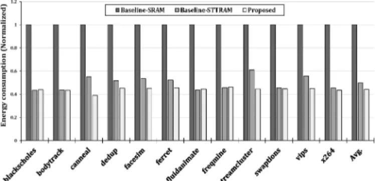
Figure 6 shows the results of energy consumption for each PARSEC application. As shown in this figure, the proposed design reduces energy consumption by about 56% on average compared to the Baseline-SRAM design, and about 11 % on average compared to the Baseline-STTRAM design. The near zero leakage power of the STT-RAM banks provides a great opportunity for lowering the energy of stack 3D memory architecture. As a result, Baseline-STTRAM consumes less energy than Baseline-SRAM, however, our hybrid memory design also reduces average energy consumption of Baseline STTRAM design.
Fig. 6. Normalized energy consumption of each benchmark application with respect to the Baseline-SRAM .
Figure 7 shows life time of the proposed memory architecture for each benchmark with respect to the baseline. Note that in this figure, the baseline is a memory architecture with only STT-RAM banks. In this figure. We assumed the endurable maximum write number for SRAM and different NVM memory technologies based on Table IV [28].
TABLE IV. COMPARISON OF MAXIMUM WRITE NUMBER FOR VARIOUS MEMORY TECHNOLOGIES
To evaluate lifetime, we assumed that each benchmark continuously run until one of the cache blocks exceeds the number of maximum endurable writes (shown in Table IV) in each memory bank. As shown in this figure, life time of our proposed heterogeneous memory architecture is higher than the baseline for all benchmarks. More specifically, our hybrid memory design yields an 8.3 x (on average) up to 51.28 x improvement in life time in comparison with baseline memory design. Thus, our hybrid memory structure results more reliable 3D stacked memory structure and this is due to allocating write intensive data blocks to SRAM and read intensive data blocks into STT-RAM banks based on compiler directed approach.
Fig. 7. Normalized life time for each application with respect to the proposed method.
V. CONCLUSION
In this work, we proposed a model to design a minimum energy heterogeneous memory system with using SRAM and STT-RAM memory banks. The key idea of our work is exploiting compiler to distribute data blocks into SRAM and STT-RAM banks. For this target, we modeled our work as a convex optimization problem. Our work reduces energy consumption of 3D stacked memory while it improves life time of the memory design. Experimental results show that the proposed method reduces energy consumption by 56% on average compared to the traditional memory designs, and improves life time of the proposed architecture up to 51.28 times in comparison with Baseline-STTRAM design.
REFERENCES
[1] J. Kao, S. Narendra and A. Chandrakasan, "Subthreshold leakage modeling and reduction techniques," In the 2002 IEEE/ACM international conference on Computer-aided design(ICCAD), pp. 141-148,2002.
[2] W. Wang and P. Mishra, "System-wide leakage-aware energy minimization using dynamic voltage scaling and cache reconfiguration in multitasking systems," IEEE Trans?�t;onc on \I pc" Large Scale
Integration (VLSI) Systems, vol. 20, pp. 902 - 910, 2012.
[3] X. Guo, E. Ipek and T. Soyata, "Resistive computation: avoiding the power wall with low-leakage, STT-MRAM based computing," In ISCA, pp. 371-382, 2010.
[4] A. K. Mishra, T. Austin, X. Dong, G. Sun, Y. Xie, N. vijaykrishnan and C. R. Das, "Architecting on-chip interconnects for stacked 3D STT RAM caches in CMPs," In ISCA, pp. 69-80, 2011.
[5] J. Meng, and A. K.Coskun, "Analysis and runtime management of 3D systems with stacked DRAM for boosting energy efficiency," Design, Automation & Test in Europe Conference & Exhibition (DATE), pp. 611- 616, 2012.
[6] Y.-T. Chen, J. Cong, H. Huang, B. Liu, C. Liu, M. Potkonjak and G. Reinman. "Dynamically reconfigurable hybrid cache: An energy efficient last-level cache design. " In DATE, pages 45-50, 2012. [7] Z. Wang, D. A. Jimenez, C. Xu and G. Sun and Y. Xie, "Adaptive
Placement and Mir.ration Policv for an STT-RAM-Rased Hvhrid Cache," In High Performance Computer Architecture (HPCA), pp. 13-24,2014.
[8] H. Hajimiri, P. Mishra, S. Bhunia, B. Long, Y. Li and R. Jha,"Content aware encoding for improving energy efficiency in multi-level cell resistive random access memory," In), IEEE/ACM International Symposium on Nanoscale Architectures (NANOARCH). pp. 76-81, 2013.
[9] C. Fu, M. Zhao, C. J. Xue and Alex Orailoglu. "Sleep-aware variable partitioning for energy-efficient hybrid PRAM and DRAM main memory," In Proceedings of the international symposium on Low power electronics and design, pp. 75-80, 2014.
[10] Z W"n" n A Jimenez r XII r. SlIn "ncl Y Xie "AcI"ntive nl"cement
and migration policy for an STT-RAM-based hybrid cache," In 20th International Symposium on High Performance Computer Architecture (HPCA), pp. 13-24,2014.
[11] Y. Li, Y. Zhang, H. Li, Y. Chen, and A. K. Jones, "CIC: A configurable, compiler-guided STT-RAM L I cache," ACM Trans. Architec. Code Optim. vol. 10, issue. 4, 22 pages, 2013.
[12] Y. Li and A. K. Jones, "Cross-layer Techniques for Optimizing Systems Utilizing Memories with Asymmetric Access Characteristics," IEEE Computer Society Annual Symposium on VLSI (ISVLSI), pp. 404-409, 2012.
[13] Y. Chen, J. Cong, H. Huang, C. Liu, R. Prabhakar, and G. Reinman, "Static and Dynamic Co-Optimizations for Blocks Mapping in Hybrid Caches," (ISLPED), pp. 237-242,2012.
[14] 1. Hu, Q. Zhuge, C. 1. Xue, W. Tseng, and E. H. M. Sha, "Management and optimization for nonvolatile memory-based hybrid scratchpad memory on multicore embedded processors," ACM Transactions on Embedded Computing Systems (TECS), vol. 13, Issue. 4, Article 79, 25 pages, 2014.
[IS] O. Ozturk, and M. Kandemir, "ILP-based energy minimization techniques for banked memories," ACM Trans. Des. Autom. Electron. Syst, vol. 13, Issue. 3, Article 50, 40 pages, 2008.
[16] M. Grant, S. Boyd and Y. Ye, "CVX: Matlab software for disciplined convex programming," Available at www.stanford.edu/ boyd/cvx/. [17] Z. Wang, D. A. Jimenez, C. Xu, G. Sun, and Y. Xie, "Adaptive placement
and migration policy for an STT-RAM-based hybrid cache," In High Performance Computer Architecture (HPCA), pp. 13-24,2014. [18] 1. Ahn, S. Yoo, and K. Choi, "Prediction Hybrid Cache: An Energy
Efficient STT-RAM Cache Architecture," IEEE Transaction on Computer, 2015.
[19] A. Valero, 1. Sahuquillo, S. Petit, P. Lopez, and 1. Duato. "Design of Hybrid Second-Level Caches," IEEE Transaction on Computers, vol. 64, no. 7, 2015.
[20] Z. Zhou, 1. Ju, Z. Jia, and X. Li. "Managing hybrid on-chip scratchpad and cache memories for multi-tasking embedded systems. " In 20th Asia and South Pacific Design Automation Conference (ASP-DAC' IS), pp. 423-428,20 IS.
[21] N. Binkert, B. Beckmann, G. Black, S. K. Reinhardt, A. Saidi, A. Basu, J. Hestness et al. "The gemS simulator. " ACM SIGARCH Computer Architecture News 39, vol. 39, no. 2, May 20 II.
[22] X. Dong, C. Xu, N. Jouppi, and Y. Xie, "NVSim: A Circuit-Level Performance, Energy, and Area Model for Emerging Non-volatile Memory," In Emerging Memory Technologies Springer, pp. IS-50, New York, 2012.
[23] N. Muralimanohar, R. Balasubramonian and N. P. Jouppi, "CACTI 6.0: A tool to model large caches," HP Laboratories, Technical Report, 2009. [24] M. Palesi, S. Kumar and D. Patti, "Noxim: Network-on-chip simulator,"
http://noxim.sourceforge.net, 2010.
[25] S. Li, J. H. Ahn, R. D. Strong, J. B. Brockman, D. M. Tullsen, and N. P. Jouppi, "McPAT: an integrated power, area, and timing modeling framework for multicore and manycore architectures," In Annual IEEE/ACM International Symposium on MICRO, pp. 469-480, 2009. [26] M. Gebhart, J. Hestness, E. Fatehi, P. Gratz, and S. W. Keckler,
"Running PARSEC 2.1 on MS. " University of Texas at Austin, Department of Computer Science, Technical Report, 2009.
[27] C. Lattner and V. Adve, "LL VM: A compilation framework for lifelong program analysis & transformation," in Proc. lnt. Symp. Code Generat. Optim., Feedback-Directed Runtime Optim. , pp. \-12,2004.
[28] M. T. Chang, P. Rosenfeld, S. L. Lu, B. Jacob, "Technology comparison for large last-level caches (L3Cs): Low-leakage SRAM, low write energy STT-RAM, and refresh-optimized eDRAM," In High Performance Computer Architecture (HPCA20 13), IEEE 19th International Symposium on. IEEE, 2013.
[29] Y. T. Chen, J. Cong , H. Huang, B. Liu, C. Liu, M. Potkonjak, and G. Reinman, "Dynamically reconfigurable hybrid cache: An energy efficient last-level cache design," In Design, Automation & Test in Europe Conference & Exhibition (DATE), pp. 45-50, 20 12.