High-performance solar-blind AlGaN photodetectors
Ekmel Ozbay,
aTurgut Tut,
aand Necmi Biyikli
ba
Department of Physcis, Bilkent University, Bilkent, Ankara 06800 TURKEY
b
Department of Electrical Engineering, Virginia Commonwealth University, Richmond, VA 23284 U.S.A.
ABSTRACT
Design, fabrication, and characterization of high-performance AlxGa1-xN-based photodetectors for solar-blind
applications are reported. AlxGa1-xN heterostructures were designed for Schottky, p-i-n, and metal-semiconductor-metal
(MSM) photodiodes. The solar-blind photodiode samples were fabricated using a microwave compatible fabrication process. The resulting devices exhibited extremely low dark currents. Below 3 fA leakage currents at 6 V and 12 V reverse bias were measured on p-i-n and Schottky photodiode samples respectively. The excellent current-voltage (I-V) characteristics led to a detectivity performance of 4.9×10¹⁴ cmHz1/2W-1. The MSM devices exhibited photoconductive
gain, while Schottky and p-i-n samples displayed 0.15 A/W and 0.11 A/W peak responsivity values at 267 nm and 261 nm respectively. All samples displayed true solar-blind response with cut-off wavelengths smaller than 280 nm. A visible rejection of 4×10⁴ was achieved with Schottky detector samples. High speed measurements at 267 nm resulted in fast pulse responses with >GHz bandwidths. The fastest devices were MSM photodiodes with a maximum 3-dB bandwidth of 5.4 GHz.
Keywords: AlGaN, detectivity, heterostructure, high-speed, MSM, photodetector, p-i-n, Schottky, solar-blind, UV.
1. INTRODUCTION
The sun is a strong source of ultraviolet (UV) radiation. Thanks to the ozone layer, we are not exposed to the harmful portion of the solar UV radiation. The ozone layer acts as a natural low-pass filter by absorbing the high-energy solar photons with wavelengths smaller than ∼280 nm [1]. Photodetectors which respond only to radiation with λ<280 nm are defined as solar-blind photodetectors. Within the atmosphere, such a detector would not detect any solar radiation. Hence, if a solar-blind photodetector detects a signal, it should originate from an external UV emitter (flame, missile plume, etc.) [2].
The immunity from solar interference makes solar-blind detectors unique for a wide range of commercial and military applications: environmental (ozone layer) monitoring, flame detection/fire alarms, sterilization/detection of biological and chemical agents, engine monitoring, missile plume detection, secure intersatellite communications, and underwater/sub-marine communication systems [3]. These applications require high-performance solar-blind photodetectors with low dark current, high responsivity, high detectivity, and high bandwidth.
Solar-blind detection was traditionally accomplished by photomultiplier tubes (PMTs) and silicon photodiodes. With the advent in material growth of high-quality AlxGa1−xN ternary alloys [4]−[14], AlGaN-based wide bandgap
solar-blind photodetectors emerged as a potential alternative for the PMT and Si-based detector technology. The long-wavelength cut-off of AlxGa1−xN can be tuned from 360 to 200 nm by increasing the Al content and for x>0.38, AlGaN
becomes intrinsically solar-blind. Therefore, unlike PMT and Si technology, AlGaN-based solar-blind detectors do not need complex and costly filters. In addition, they can operate under harsh conditions (high temperature and power levels) due to their wide band gap and robust material properties [15]. These features made the AlxGa1−xN material
system the choice for the realization of high-performance solar-blind detectors.
The first based solar-blind photodetectors were demonstrated in 1996 [16], [17]. Both detectors were AlGaN-based photoconductors with true solar-blind characteristics. Thereafter, several research groups have contributed to the performance of solar-blind AlGaN photodetectors. Schottky [18]−[23], p-i-n [24]−[38], MSM [39]−[44], and p-n junction [45] type of photodiodes with excellent detection characteristics were reported. Very low dark currents at the fA level [22], [35], [36], [39] and high solar-blind responsivity performance [29], [33], [37] resulted in extremely high detectivity values which could not be achieved with conventional narrow bandgap semiconductor based detectors. High visible rejection of more than 6 orders of magnitude [25], [45], and low cut-off wavelengths down to 225 nm [25] were
also successfully reported. Noise performance of high quality solar-blind AlGaN detectors are far beyond the limit of the state of the art measurement set-ups. In terms of high-speed performance, AlGaN solar-blind detectors with GHz-level frequency response have been reported recently [22], [23].
In this paper, we present our research efforts on high-performance AlGaN-based solar-blind photodiodes. Schottky, p-i-n, and MSM structures were designed, fabricated and characterized. Solar-blind detectors with record dark current density, solar-blind detectivity, and 3-dB bandwidth performance are demonstrated.
2. EXPERIMENTAL WORK
2.1 Design
The epitaxial structures of AlGaN photodiodes were designed to achieve true solar-blindness with cut-off wavelengths smaller than 280 nm. To fulfill this requirement, AlxGa1−xN absorption layers with x > 0.38 were utilized. Table 1(a)
shows the layer structure of AlGaN Schottky photodiode. The active layer is a 0.8 µm thick Al0.38Ga0.62N layer. A
highly doped GaN layer was used for ohmic contact region due to the difficulty of obtaining high-quality ohmic contacts with AlxGa1-xN layers. The n-type doped 0.2 µm thick Al0.38Ga0.62N layer acted as a diffusion barrier for the
photo-carriers generated in the GaN ohmic contact layer. This diffusion barrier was inserted to increase the visible rejection of the detector.
The AlGaN p-i-n photodiode was also designed for front illumination. The epitaxial structure of the p-i-n detector is shown in Table 1(b). The main disadvantage of AlGaN-based p-i-n detectors is the difficulty of forming high quality ohmic contacts to p-type doped AlGaN layers. To minimize this difficulty, a thin p+ GaN cap layer was added on top of p+ AlGaN layer. This cap layer reduces the quantum efficiency performance by absorption, and makes the detector slower by the diffusion of photogenerated carriers. However, these drawbacks can be cancelled by the recess etch of the cap layer after device fabrication. To minimize carrier trapping at the p+ GaN/AlGaN interface, a thin grading layer was designed. The absorption layer used in p-i-n structure was formed by a 100 nm thick unintentionally doped Al0.45Ga0.55N layer. For n+ ohmic contacts, similar to Schottky design, an n-type doped GaN layer was used.
Two structures with different Al-compositions were designed for solar-blind MSM detectors. The detector active layers consisted of ∼1.0 µm thick unintentionally doped Al0.38Ga0.62N and Al0.6Ga0.4N layers respectively, which were
grown on top of ∼2.0 µm thick GaN templates. All four AlxGa1-xN/GaN epitaxial layers of the hetero-junction
photodiode wafers were grown on 2-inch (0001) sapphire substrates using metal-organic chemical vapor deposition (MOCVD).
Material Thickness Doping (cm−3)
Al0.38Ga0.62N 0.8 µm N− (1×1016 cm−3) Al0.38Ga0.62N 0.2 µm N+ (2×1018 cm−3) GaN 0.6 µm N+ (2×1018 cm−3 ) GaN 0.5 µm u. i. d.
AlN nucleation layer <100 nm u. i. d. Sapphire substrate ∼300 µm −
Material Thickness Doping (cm−3)
GaN 30 nm P+ (>1×1017 cm−3 ) Al0.45Ga0.55N → GaN 15 nm P+ (>1×1017 cm−3) Al0.45Ga0.55N 10 nm P+ (>1×1017 cm−3) Al0.45Ga0.55N 100 nm u. i. d. GaN 250 nm N+ (2×1018 cm−3 ) AlN nucleation layer 100 nm u. i. d.
Sapphire substrate ∼300 µm −
(a) (b) Table 1: Epitaxial layer structure of (a) AlGaN Schottky photodiode (b) AlGaN p-i-n photodiode.
2.2 Fabrication Process
A five-level microwave compatible fabrication process was used for Schottky and p-i-n photodiode samples [22], [46], [36]. MSM detector samples were fabricated by using four mask levels. For Schottky and p-i-n samples, the fabrication started with the formation of n+ ohmic contacts. First, the ohmic patterns were defined and etched down to the n+ GaN layer. Dry etching with CCl2F2 gas was utilized in a reactive ion etching (RIE) system. Ti/Al alloy was evaporated and
after lift-off process, thermal annealing at 700 oC was applied for 30 seconds in a rapid thermal annealing (RTA) system. The second step was the Schottky contact and p+ ohmic contact formation for Schottky and p-i-n samples respectively. A thin (∼100 Å) Au film was deposited as Schottky contact on Al0.38Ga0.62N layer. p+ ohmic contacts were
formed by Ni/Au metallization on p+ GaN layer, followed by the same annealing process used for n+ contacts. Then the device mesas, ranging from 30 µm to 200 µm in diameter, were defined and isolated via RIE process. Afterwards, a
∼100 nm thick Si3N4 layer was deposited using plasma enhanced chemical vapor deposition to passivate the sample
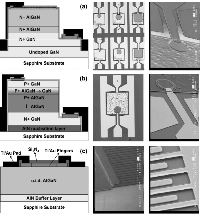
Ti/Au metallization. The fabrication process of MSM photodiode samples started with the metallization of interdigitated back-to-back Schottky metal fingers. This was followed by mesa etch, surface passivation, and finally interconnect metallization. MSM photodiodes with equal finger spacings and widths varying between 3 and 10 µm were fabricated. The device mesas had an active area of 100×100 µm2. Cross-sectional schematics and microphotographs of completed photodiode samples are shown in Fig. 2.
Figure 1: Cross-sectional schematics, optical microscope photographs and scanning electron microscopy images of fabricated solar-blind detector samples: (a) AlGaN Schottky photodiode (b) AlGaN p-i-n photodiode (c) AlGaN MSM photodiode.
2.3 Characterization
After device fabrication, I-V, spectral responsivity, and high-speed characterizations were carried out. All measurements were made on-wafer, using a microwave probe station. To observe the electrical diode characteristics and the leakage current of the solar-blind AlGaN photodiodes, we first performed the I-V measurements. The measurement setup consisted of a high-resistance Keithley 6517A electrometer, DC probes with triax output and low-noise triax cables. DC current was measured as voltage was applied to the devices.
Spectral responsivity measurements were done using a 175 W xenon light-source, 1/4 m Digikrom DK240 monochromator, multi-mode UV fiber, DC voltage source, SR830 DSP lock-in amplifier and a Newport model 1830-C calibrated optical power-meter. Xenon lamp output was fed into the monochromator. The monochromator output was chopped and coupled to a multimode UV fiber using a UV-enhanced focusing lens. The detectors were illuminated by the optical output coming out from the fiber which was calibrated using the calibrated photodetector. The detectors were biased with a DC voltage source up to 50 V, and the resulting photocurrent was measured using the lock-in amplifier.
Temporal high-frequency measurements were done at the solar-blind wavelength of 267 nm. Ultrafast UV pulses were generated using a laser set-up with two nonlinear crystals.A Coherent Mira 900F model femtosecond mode-locked Ti:sapphire laser was used to generate the pump beam at 800 nm. The pump pulses were produced with 76 MHz repetition rate and 140 fs pulse duration. These pulses were frequency doubled to generate a second harmonic beam at 400 nm using a 0.5 mm thick type-I β-BaB2O4 (BBO) crystal. The second harmonic beam and the remaining part of the pump beam were frequency summed to generate a third harmonic output beam at 267 nm using another type-I BBO crystal with thickness of 0.3 mm. The resulting 267 nm pulses had pulsewidths below 1 ps and were focused on to the devices using UV-enhanced mirrors and lenses. The detectors were biased using a DC voltage source and a 26 GHz bias-tee. Using 40 GHz microwave probe and cables, the electrical pulses were transferred to a 20 GHz sampling oscilloscope where the temporal pulse responses were observed.
3. RESULTS & DISCUSSION
3.1. Current-Voltage
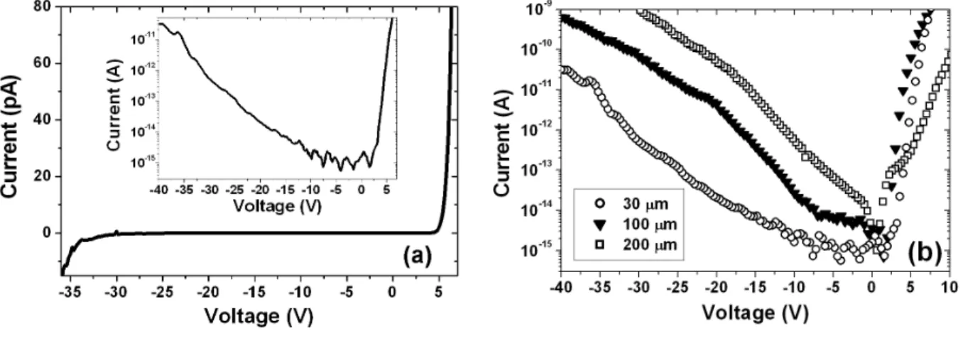
Figure 2: I-V curves of AlGaN Schottky photodiode samples. (a) 30 µm diameter device (inset shows the measurement data in logarithmic scale) (b) I-V curves of 30 µm, 100 µm, and 200 µm solar-blind detectors.
All four detector samples exhibited excellent I-V characteristics with low dark current and high breakdown voltages. The good I-V results indicate the quality of growth and fabrication processes. Figure 2(a) shows the measured I−V curve of a small area (30 µm diameter) device. The solar-blind device exhibited leakage current less than 3 fA and 10 fA for reverse bias up to 12 V and 17 V respectively. Under < 12 V reverse bias, the measured dark current fluctuated below the 3 fA level due to the background noise of the setup. Sub-fA leakage currents were observed in this range. Using an exponential fit, we estimate the zero bias dark current less than 0.1 fA. The corresponding dark current density for this device at 12 V was 4.2×10⁻¹⁰ A/cm2. Typical reverse breakdown voltages were measured to be higher than 50 V. The dependence of dark current on device area is shown in Fig. 2(b). Leakage current increased with device area as
expected. To compare these results, the current density values at 5V reverse bias were calculated. 100 µm and 200 µm devices exhibited 7 fA and 67 fA dark current at −5 V, which led to 8.9×10⁻¹¹ A/cm2 and 2.1×10⁻¹⁰ A/cm2 dark current density values respectively. Due to the experimental setup limit, the actual dark current density of 30 µm device at 5 V reverse bias could only be estimated by exponential fitting curve as 3.3×10⁻¹¹ A/cm2. These results correspond to the lowest leakage performance reported for AlGaN-based Schottky photodiodes.
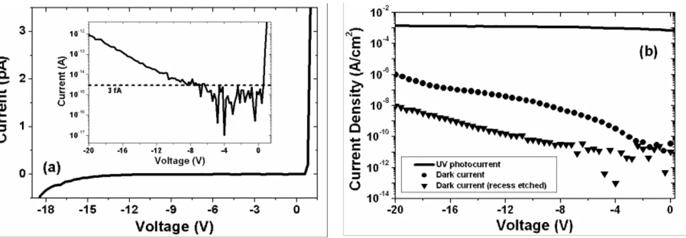
Figure 3: (a) Dark current of a 100x100 µm2 solar-blind AlGaN photodiode. The inset shows the same plot in logarithmic scale. (b) Dark current density before/after recess etch and UV photocurrent under 267 nm illumination.
AlGaN p-i-n photodiodes also exhibited low dark current. With the removal of top p+ GaN cap layer, dark current values went down to a few fA. Figure 3(a) shows the measured dark current of a 100×100 µm2 device after recess etch. For reverse bias values smaller than 6 V, the measured dark current fluctuated below the 3 fA level, which corresponds to a dark current density smaller than 3.0×10⁻¹¹ A/cm2. Dark current was below 7 fA for reverse bias values up to 10 V.
The measured forward turn-on voltages were small (∼1 V) and reverse breakdown behavior was observed for reverse bias values over 40 V.
Figure 3(b) shows the dark current density measured before and after recess etch and the UV photocurrent generated by the photodiode under 267 nm illumination. The strong UV photocurrent shows that the detectors are operating in solar-blind spectrum. I-V measurements showed that the dark current dropped by over 2 orders of magnitude after the GaN cap layer was removed. This result was well expected since the lower band gap GaN layer generates more carriers due to thermal generation. Nevertheless, the dark current of the sample without recess etching was also low: below 10 fA at 3 V reverse bias.
Figure 4: (a) I-V measurement of a 10 µm finger width/spacing Al0.6Ga0.4N MSM photodiode. (b) Dark current
I-V measurement of the AlGaN MSM samples resulted in low dark current with very high breakdown voltages. As expected, due to its larger bandgap, lower leakage and higher breakdown voltages were measured with Al0.6Ga0.4N
MSM samples as compared to Al0.38Ga0.62N MSM devices. Figure 4(a) shows the dark current of an Al0.6Ga0.4N MSM
detector with 10 µm finger width/spacing. The dark current was less than 100 fA up to +/−200 V bias voltage. Figure 4(b) shows the dark current measurement of the same device upto 300 V. Leakage current is kept below 10 fA in the (−50 V, +100 V) range. No sign of breakdown characteristic was observed till 300 V. Al0.38Ga0.62N MSM detectors had
higher dark currents, reaching ∼1 nA around 55 V, and lower breakdown voltages at ∼80 V.
3.2. Spectral Photoresponse
Spectral photoresponse measurements of the AlGaN photodiodes were carried out in the 250-400 nm spectral range. Bias-dependent spectral responsivity with true solar-blind characteristics was observed in all detector samples. All samples have exhibited true solar-blind operation. However, the cut-off characteristic of the p-i-n sample was not as good as Schottky and MSM devices.
Figure 5: (a) Measured spectral responsivity curves of solar-blind AlGaN Schottky photodiode samples as a function of reverse bias voltage. (b) Corresponding spectral quantum efficiency measurement.
Figure 5(a) shows the measured spectral responsivity of a solar-blind AlGaN Schottky photodiode under different bias conditions. A strong bias dependence is observed: device responsivity increased with applied reverse bias. The peak reponsivity increased from 61 mA/W at 250 nm to 147 mA/W at 256 nm when applied reverse bias was increased from 5 V to 20 V. The device responsivity saturated for > 20 V reverse bias, which indicates the total depletion of undoped Al0.38Ga0.62N absorption layer. A sharp decrease in responsivity was observed at ∼265 nm. The cut-off
wavelength of the detectors was found as ∼267 nm, which ensured the true solar-blind operation of our detectors. Fig. 5(b) shows the semi-log plot of the corresponding spectral quantum efficiency. A maximum efficiency of 71% at 256 nm was measured under 20 V reverse bias. The visible rejection reached a maximum of ∼4×10⁴ at 10 V reverse bias.
The spectral responsivity measurements of AlGaN p-i-n sample were completed in several steps, as the absorbing GaN cap layer was etched step by step. The measurement results obtained before recess-etch process are shown in Fig. 6(a). The device efficiency increased with applied reverse bias. Zero-bias peak efficiency of 22% at 267 nm improved to 43% at 271 nm for 20 V reverse bias. Quantum efficiency did not increase for higher reverse bias values, which indicates that the undoped Al0.45Ga0.55N active layer was totally depleted at 20 V. The corresponding peak responsivity
under full depletion was 95 mA/W at 271 nm. The cut-off wavelength of the p-i-n devices was around 283 nm. A visible rejection of ∼ 4 orders of magnitude was achieved at zero bias (see inset figure). The cut off was rather smooth: 3 order of magnitude rejection was reached within 100 nm.
To observe the effect of p+ GaN cap layer removal, this layer was recess etched in several steps. The corresponding responsivity curves at 10 V reverse bias for each etch step are shown in Fig. 6(b). As the p+ GaN cap layer was recess etched, less absorption loss within this layer resulted in higher device responsivity. p+ GaN layer was completely etched in three etch steps. The peak responsivity improved from 81 mA/W to 111 mA/W, while the peak wavelength changed from 271 nm to 261 nm. The peak quantum efficiency performance achieved after 3 etch steps was 53% at 261 nm.
Figure 6: (a) Spectral quantum efficiency and the corresponding responsivity curve of the non-etched solar-blind AlGaN p-i-n detector. (b) Spectral responsivity as a function of recess etch of the p+ GaN cap layer.
Figure 7(a) shows the measured spectral responsivity curves for an Al0.38Ga0.62N MSM photodiode. The
corresponding spectral quantum efficiency under 2 V bias is plotted in Fig. 7(b). At this bias voltage, the PD had a peak quantum efficiency of 40% at 264 nm. The solar-blind MSM photodiodes displayed true solar-blind photoresponse with a cut-off wavelength of 272 nm. Photoconductive gain mechanism dominated the photoresponse for relatively low bias voltages. The peak responsivity under 6 V bias was measured as 1.26 A/W at 264 nm, corresponding to an external quantum efficiency of ∼600%. The photoconductive gain in AlGaN MSM photodiodes can be explained by the presence of hole-trapping sites due to threading dislocations [48]. Holes are accumulated at the trap sites, increasing the electron injection at the cathode. This injection results in photoconductive gain which is proportional to the electric field between the electrodes.
Figure 7: (a) Measured spectral responsivity curves of Al0.38Ga0.62N MSM photodiodes as a function of bias voltage. (b)
Linear-scaled plot of the corresponding spectral quantum efficiency under 2 V bias.
A sharp drop in responsivity around 275 nm was observed. A visible rejection of nearly 3 orders of magnitude was obtained at 350 nm. The rejection at longer wavelengths was measured using continuous wave Ar laser lines. Under zero bias, at 458 nm (the shortest line of Ar), the rejection was measured as 2×10⁴. For Al0.6Ga0.6N MSM sample, the
quantum efficiency reached a maximum of 60% at 250 nm, corresponding to a device responsivity of 0.12 A/W. The cut-off was around 255 nm, well below 280 nm. The visible rejection reaches 8×10⁴ at 420 nm.
3.3. Detectivity
Based on the fact that the background radiation is very small with respect to the thermal noise within the solar-blind spectrum, we can safely assume that the detectivity of solar-blind detectors is thermally limited. Therefore, neglecting
the background radiation component, the thermally limited specific detectivity can be calculated by D*=Rλ(R0A/4kT)1/2,
where Rλ is the photovoltaic device reponsivity, R0 is the dark impedance at zero bias which is also known as
differential resistance, and A is the detector area [49]. To calculate the thermally limited specific detectivity of our samples, R0 was determined by fitting the dark current data with curve fitting method [50].
Figure 8: (a) Linear plot of I-V data and exponential fit for a 30 µm diameter solar-blind AlGaN Schottky photodiode. (b) Calculated differential resistance for the same device.
Figure 8(a) shows the measured and exponentially fitted I-V curves for a 30 µm diameter AlGaN Schottky photodiode. A good fit to the experimental data for reverse bias less than 15 V was achieved. The differential resistance was calculated by taking the derivative (dV/dI) of the resulting curve, which is shown in Fig. 4(b). The extremely low sub-fA dark currents resulted in very high resistance values. A maximum resistance of 5.44×10¹⁷Ω was obtained at 0.6 V. Zero-bias differential resistance, R0 was slightly lower: 4.01×10¹⁷Ω. These resistance values are ∼2 orders higher
than previously reported solar-blind AlGaN detectors. Combining with Rλ=1.4 mA/W, A=7.07×10⁻⁶ cm2, and T=293 K, we achieved a detectivity performance of D*= 1.83×10¹³ cmHz1/2/W−1 at 250 nm. The detectivity was mainly limited by the low photovoltaic (zero bias) responsivity of the device.
Figure 9: Exponential curve fitting to the measured dark current of a 100x100 µm2 AlGaN p-i-n device. Inset figure shows the reverse and forward bias part fitting curves separately in a semi-log plot.
Figure 9 shows the dark current measurement data of a 100×100 µm2 device and the exponential fitting curve in both logarithmic and linear scale. By taking the derivative (dV/dI) of the resulting curve equation at zero bias, we obtained a differential resistance of R0= 9.52×10¹⁵Ω. This value was much higher than the resistivity of low-quality p-type ohmic
contacts. Combining with Rλ=65 mA/W, A=10−4 cm2, and T=293 K, we achieved a thermally-limited detectivity performance of D*= 4.9×10¹⁴ cmHz1/2/W−1 at 267 nm. This result shows that the room-temperature solar-blind detectivity performance of these AlGaN p-i-n photodiodes exceed the typical detectivity performance of a cooled PMT detector [51].
Similar procedure was applied to MSM samples. As expected, lower detectivities were obtained for these samples mainly due to the higher leakage current and lower photovoltaic responsivity. Detectivity values of 8.9×10¹⁰ cmHz1/2W−1 at 264 nm were achieved with Al0.38Ga0.62N MSM photodiodes.
3.4. Speed
Time-domain high-speed characterization of the solar-blind detector samples resulted in fast pulse responses with high 3-dB bandwidths. The detector pulse responses were bias dependent. The fastest pulses were produced by small-area devices. Very short rise times were observed. The response speed of the devices was limited by the slow decay tails.
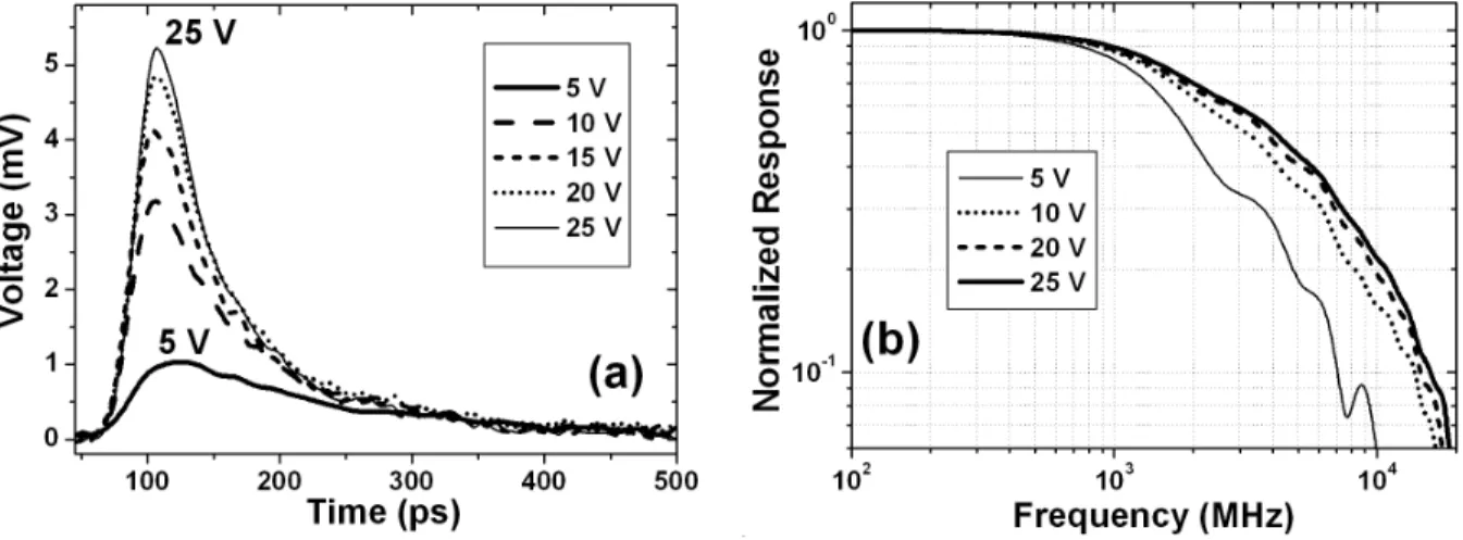
Figure 10(a) shows the pulse response of a 30 µm diameter AlGaN Schottky photodiode as a function of applied reverse bias. Faster pulses with higher pulse amplitudes were obtained with increasing reverse bias as the n− AlGaN absorption layer was fully depleted under high reverse bias voltages. The pulse-width decreased from 80 ps to 53 ps as bias was changed from 5 V to 25 V. The drop in full-width-at-half-maximum (FWHM) was mainly caused by the decrease in fall time. Short rise times of ∼26 ps were measured. Rise time did not change significantly with bias since it was close to the measurement limit of the 20 GHz scope. The corresponding FFT curves are plotted in Fig. 10(b). As expected, 3-dB bandwidth values increased with reverse bias. A maximum 3-dB bandwidth of 4.1 GHz was achieved at 25 V.
Figure 10: (a) High-speed pulse response of a 30 µm diameter AlGaN Schottky device as a function of applied reverse bias. (b) Corresponding FFT curves of the temporal data.
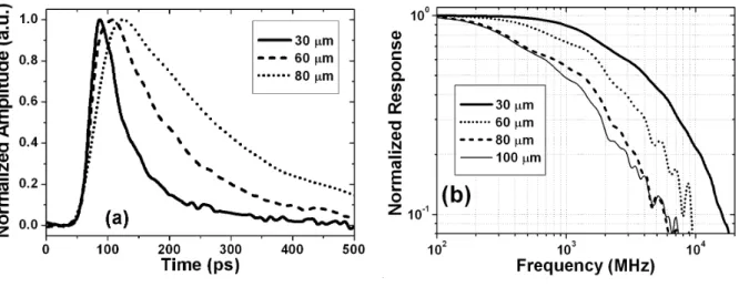
Figure 11(a) shows the normalized pulse responses displayed by detectors with different device areas. All measurements were taken under 25 V reverse bias. Larger device area resulted in slower pulse response, which can be explained by the increased RC time constant. The corresponding frequency response curves are shown in Fig. 11(b). 3-dB bandwidth dropped to 0.95 GHz for 100 µm diameter device.
Mainly three speed limitations exist for photodiodes fabricated on defect-free materials: transit time across the depletion region, RC time constant, and diffusion of photogenerated carriers in low-field regions. The fabricated AlGaN Schottky detectors do not suffer from carrier diffusion. The only limitation comes from RC time constant. This makes sense since the series resistance of these devices was high. If RC time constant was the only limitation for our devices, we should be able to fit the fall time components with a simple exponential decay function. However, a reasonable exponential fit with a single time constant could not be achieved. Instead, responses were fitted well with second order exponential decay functions, i.e. with a sum of two exponential decay functions with two different time constants. This
shows that another limitation factor exists in our devices. We believe that the additional and slower decay tail was originated by the carrier trapping effect. Photogenerated carriers can be trapped at the defects/trapping-sites in the AlGaN active layer, which are formed during the crystal growth process. The slower portion of the decay tail is possibly formed by the late arrival of the released carriers which were trapped in these sites.
Figure 11: (a) Normalized high-speed pulse response data for solar-blind AlGaN Schottky detectors with different areas. (b) Corresponding frequency response curves.
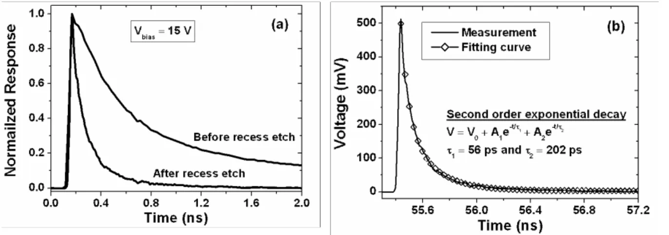
High-speed measurements for the AlGaN p-i-n sample were done before and after recess etch. Fig. 12(a) and (b) show the measured pulse response data of a 30 µm diameter device with and without the p+ GaN cap layer respectively. The calculated FFT curves are also plotted. Parallel to theoretical expectations, faster response and higher 3-dB bandwidths were obtained after the removal of GaN cap layer. The p+ GaN layer is a low-field region, in which carriers move by diffusion. The minority carrier (electrons) diffusion mechanism limits the bandwidth of the non-etched p-i-n detector. After the removal of GaN cap layer, the decay tail was reduced significantly: fall time decreased from 2.49 ns to 290 ps under 15 V reverse bias. At the same time, FWHM was improved from 384 ps to 71 ps. The detectors responded faster under higher reverse biases. FWHM values of 115 ps and 71 ps were measured for reverse bias values of 2 V and 15 V respectively. The fastest results were obtained at 15 V reverse bias. 3-dB bandwidths achieved at 15 V bias were 160 MHz and 1.65 GHz for as-grown and recess-etched samples.
Figure 12: (a) Pulse response of a 30 µm diameter AlGaN p-i-n photodiode before recess etch. Inset shows the FFT of temporal data. (b) Normalized pulse response of the same device after recess etch. The corresponding frequency response is shown in the inset figure.
To make a better comparison, 15 V pulse responses are plotted in Fig. 13(a). Also, an exponential decay fit was applied the recess etched device response. A good fit was accomplished using a second order exponential decay with time constants of 56 and 202 ps (Fig. 13(b)).
Figure 13: (a) Pulse response of a 30 µm diameter AlGaN p-i-n photodiode before recess etch. Inset shows the FFT of temporal data. (b) Normalized pulse response of the same device after recess etch. The corresponding frequency response is shown in the inset figure.
The measured pulse responses of Al0.38Ga0.62N MSM photodiodes had short rise times and exponentially decaying fall
times. Faster pulses were obtained with smaller finger spacings due to reduced carrier transit times. Therefore, the best high-speed results were achieved with 3µm devices. Pulse response measurements under different bias conditions for the 3µm device are plotted in Fig. 14(a). As expected, the pulse amplitudes had increased with applied bias voltage, due to larger photoconductive gain. Pulsewidths also increased with bias: 76, 99, 121, and 133 ps FWHM values were measured at 5, 10, 15, and 17 V bias respectively. Hence, slower responses were obtained under larger bias and gain values. This result was confirmed with the FFT analysis of the temporal data. Figure 14(b) shows the corresponding FFT curves of the measured pulse responses. A maximum 3-dB bandwidth of 5.4 GHz was achieved at 5 V bias. Bandwidth decreased with increasing bias: 3-dB bandwidths of 2.1, 1.7, and 1.5 GHz were obtained at 10, 15, and 17 V bias respectively. These values correspond to the fastest solar-blind AlGaN photodetector reported.
Figure 14: (a) Bias-dependent temporal pulse responses of an Al0.38Ga0.62N MSM photodiode with 3 µm finger
spacing. Inset shows the measured FWHM values with respect to bias voltage. (b) Corresponding FFT curves.
Pulse response measurements of Al0.6Ga0.4N MSM photodiode was done at 260 nm. The pulse response had a fast rise
time of 25 ps, but a slowly decaying fall time of 1.30 ns. FWHM of the pulse was measured as 122 ps. The corresponding 3-dB bandwidth was calculated as 150 MHz.
4. CONCLUSION
In summary, we have designed, fabricated and characterized high-performance AlGaN-based solar-blind heterojunction Schottky, p-i-n, and MSM photodiodes. True solar-blind operation was successfully demonstrated with all samples. The dark current, solar-blind detectivity, and high-speed results demonstrated in this work correspond to the best performances reported for AlGaN-based solar-blind photodetectors.
ACKNOWLEDGEMENTS
This work was supported by NATO Grant No. SfP971970, National Science Foundation Grant No. INT-9906220, Turkish Department of Defense Grant No. KOBRA-001 and Thales JP8.04
REFERENCES
1. P. Schreiber, T. Dang, G. Smith, T. Pickenpaugh, P. Gehred, and C. Litton, “Solar blind UV region and UV detector development objectives,” Proc. SPIE, vol. 3629, pp. 230−248, 1999.
2. M. Razeghi and A. Rogalski, “Semiconductor ultraviolet detectors,” J. Appl. Phys., vol. 79, pp. 7433–7473, 1996. 3. E. Monroy, “III-Nitride-based UV photodetectors,” in III-V Nitride Semiconductors Applications and
Devices, 1st ed. vol. 16, M. O. Manasreh, Ed. New York: Taylor & Francis, 2003, pp. 525–591.
4. S. Strite and H. Morkoç, “GaN, AlN, and InN: A review,” J. Vac. Science & Technol. A, vol. 10, 1237–1266, 1992.
5. H. Morkoç, S. Strite, G. B. Gao, M. E. Lin, B. Sverdlov, and M. Burns, “Large-band-gap SiC, IV nitride, and II-VI ZnSe-based semiconductor device technologies,” J. Appl. Phys., vol. 76, 1363–1398, 1994.
6. H Morkoc, A Botchkarev, A Salvador, et al., “GaN Based III-V Nitrides by Molecular Beam Epitaxy,” J. Cryst.
Growth, vol. 150, 887-891, 1995.
7. S. Sinharoy, G. Augustine, L. B. Rowland, A. K. Agarwal, R. L. Messham, M. C. Driver, and R. H. Hopkins, “Molecular beam epitaxy growth and characterization of GaN and AlxGa1 – xN on 6H-SiC,” J. Vac. Science & Technol. A, vol. 14, 896–899, 1996.
8. D. Brunner, H. Angerer, E. Bustarret, F. Freudenberg, R. Höpler, R. Dimitrov, O. Ambacher, and M. Stutzmann, “Optical constants of epitaxial AlGaN films and their temperature dependence,” J. Appl. Phys., vol. 82, 5090–5096, 1997.
9. F. Omnès, N. Marenco, B. Beaumont, Ph. de Mierry, E. Monroy, F. Calle, and E. Muñoz, “Metalorganic vapor-phase epitaxy-grown AlGaN materials for visible-blind ultraviolet photodetector applications,” J. Appl. Phys., vol. 86, 5286–5292, 1999.
10. S. C. Jain, M. Willander, J. Narayan, and R. Van Overstraeten, “III–nitrides: Growth, characterization, and properties,” J. Appl. Phys., vol. 87, 965–1006, 2000.
11. Ho Ki Kwon, C. J. Eiting, D. J. H. Lambert, B. S. Shelton, M. M. Wong, T. G. Zhu, and R. D. Dupuis, “Optical properties of undoped and modulation-doped AlGaN/GaN single heterostructures grown by metalorganic chemical vapor deposition,” J. Appl. Phys., vol. 90, 1817–1822, 2001.
12. J. P. Zhang, H. M. Wang, M. E. Gaevski, C. Q. Chen, Q. Fareed, J. W. Yang, G. Simin, and M. Asif Khan, “Crack-free thick AlGaN grown on sapphire using AlN/AlGaN superlattices for strain management,” Appl. Phys. Lett., vol. 80, pp. 3542–3544, 2002.
13. C. Q. Chen, J. P. Zhang, M. E. Gaevski, H. M. Wang, W. H. Sun, R. S. Q. Fareed, J. W. Yang, and M. Asif Khan, “AlGaN layers grown on GaN using strain-relief interlayers,” Appl. Phys. Lett., vol. 81, pp. 4961–4963, 2002. 14. T. Akasaka, T. Nishida, Y. Taniyasu, M. Kasu, T. Makimoto, and N. Kobayashi, “Reduction of threading
dislocations in crack-free AlGaN by using multiple thin SixAl1–xN interlayers,” Appl. Phys. Lett., vol. 83, pp. 4140–
4142, 2003.
15. J. C. Carrano, T. Li, P. A. Grudowski, R. D. Dupuis, and J. C. Campbell, “Improved detection of the invisible,”
IEEE Circuits & Devices Mag., Vol. 15, pp. 15–24, 1999.
16. D. Walker, X. Zhang, P. Kung, A. Saxler, S. Javapour, J. Xu, and M. Razeghi, “AlGaN ultraviolet photoconductors grown on sapphire,” Appl. Phys. Lett., vol. 68, pp. 2100–2101, 1996.
17. B. W. Lim, Q. C. Chen, J. Y. Yang, and M. Asif Khan, “High responsivity intrinsic photoconductors based on AlxGa1–xN,” Appl. Phys. Lett., vol. 68, pp. 3761–3762, 1996.
18. A. Osinsky, S. Gangopadhyay, B. W. Lim, M. Z. Anwar, M. A. Khan, D. V. Kuksenkov, and H. Temkin, “Schottky barrier photodetectors based on AlGaN,” Appl. Phys. Lett., vol. 72, pp. 742–744, 1998.
19. E. Monroy, F. Calle, J. L. Pau, F. J. Sanchez, E. Munoz, F. Omnes, B. Beaumont, and P. Gibart, “Analysis and modeling of AlxGa1–xN-based Schottky barrier photodiodes,” J. Appl. Phys., vol. 88, pp. 2081–2091, 2000.
20. S. L. Rumyantsev, N. Pala, M. S. Shur, R. Gaska, M. E. Levinshtein, V. Adivarahan, J. Yang, G. Simin, and M. Asif Khan, “Low-frequency noise in Al0.4Ga0.6N-based Schottky barrier photodiodes,” Appl. Phys. Lett., vol. 79,
pp. 866–868, 2001.
21. V. Adivarahan, G. Simin, G. Tamulaitis, R. Srinivasan, J. Yang, M. Asif Khan, M. S. Shur, and R. Gaska, “Indium-silicon co-doping of high-aluminum-content AlGaN for solar blind photodetectors,” Appl. Phys. Lett., vol.79, pp. 1903–1905, 2001.
22. N. Biyikli, O. Aytur, I. Kimukin, T. Tut, and E. Ozbay, “Solar-blind AlGaN-based Schottky photodiodes with low noise and high detectivity,” Appl. Phys. Lett., vol. 81, pp. 3272–3274, 2002.
23. N. Biyikli, I. Kimukin, T. Kartaloglu, O. Aytur, and E. Ozbay, “High-speed solar-blind photodetectors with indium-tin-oxide Schottky contacts,” Appl. Phys. Lett., vol. 82, pp. 2344–2346, 2003.
24. G. Parish, S. Keller, P. Kozodoy, J. P. Ibbetson, H. Marchand, P. T. Fini, S. B. Fleischer, S. P. Denbaars, U. K. Mishra, and E. J. Tarsa, “High-performance (Al,Ga)N-based solar-blind ultraviolet p-i-n detectors on laterally epitaxially overgrown GaN,” Appl. Phys. Lett., vol. 75, pp. 247–249, 1999.
25. D. Walker, V. Kumar, K. Mi, P. Sandvik, P. Kung, X. H. Zhang, and M. Razeghi, “Solar-blind AlGaN photodiodes with very low cutoff wavelength,” Appl. Phys. Lett., vol.76, pp. 403–405, 2000.
26. E. J. Tarsa, P. Kozodoy, J. Ibbetson, B. P. Keller, G. Parish, and U. Mishra, “Solar-blind AlGaN-based inverted heterostructure photodiodes,” Appl. Phys. Lett., vol.77, pp. 316–318, 2000.
27. D. J. H. Lambert, M. M. Wong, U. Chowdhury, C. Collins, T. Li, H. K. Kwon, B. S. Shelton, T. G. Zhu, J. C. Campbell, and R. D. Dupuis, “Back illuminated AlGaN solar-blind photodetectors,” Appl. Phys. Lett., vol. 77, pp. 1900–1902, 2000.
28. J. D. Brown, J. Li, P. Srinivasan, J. Matthews, and J. F. Schetzina, “Solar-blind AlGaN heterostructure photodiodes,” MRS Internet J. Nitride Semicond. Res., vol. 5, p. 9, 2000.
29. M. M. Wong, U. Chowdhury, C. J. Collins, B. Yang, J. C. Denyszyn, K. S. Kim, J. C. Campbell, and R. D. Dupuis, “High quantum efficiency AlGaN/GaN solar-blind photodetectors grown by metalorganic chemical vapor deposition,” Phys. Stat. Sol. (A), vol. 188, pp. 333–336, 2001.
30. P. Sandvik, K. Mi, F. Shahedipour, R. McClintock, A. Yasan, P. Kung, M. Razeghi, “AlxGa1–xN for solar-blind UV
detectors,” J. Crystal Growth, vol. 231, pp. 366–370, 2001.
31. G. Parish, M. Hansen, B. Moran, S. Keller, S. P. Denbaars, and U. K. Mishra, “Solar-blind p-GaN/i-AlGaN/n-AlGaN ultraviolet photodiodes on SiC substrate,” Phys. Stat. Sol. (A), vol. 188, pp. 297–300, 2001.
32. A. Hirano, C. Pernot, M. Iwaya, T. Detchprohm, H. Amano, and I. Akasaki, “Demonstration of flame detection in room light background by solar-blind AlGaN pin photodiode,” Phys. Stat. Sol. (A), vol. 188, pp. 293–296, 2001. 33. J. C. Campbell, C. J. Collins, M. M. Wong, U. Chowdhury, A. L. Beck, and R. D. Dupuis, “High quantum
efficiency at low bias AlxGa1–xN p-i-n photodiodes,” Phys. Stat. Sol. (A), vol. 188, pp. 283–287, 2001.
34. T. Li, D. J. H. Lambert, M. M. Wong, C. J. Collins, B. Yang, A. L. Beck, U. Chowdhury, R. D. Dupuis, and J. C. Campbell, “Low-noise back-illuminated AlxGa1–xN-based p-i-n solar-blind ultraviolet photodetectors,” IEEE J. Quant. Electron., vol. 37, pp. 538–545, 2001.
35. V. V. Kuryatkov, H. Temkin, J. C. Campbell, and R. D. Dupuis, “Low-noise photodetectors based on heterojunctions of AlGaN-GaN,” Appl. Phys. Lett., vol. 78, pp. 3340–3342, 2001.
36. C. J. Collins, U. Chowdhury, M. M. Wong, B. Yang, A. L. Beck, R. D. Dupuis, and J. C. Campbell, “Improved solar-blind detectivity using an AlxGa1–xN heterojunction p-i-n photodiode,” Appl. Phys. Lett., vol. 80, pp. 3754–
3756, 2002.
37. C. J. Collins, U. Chowdhury, M. M. Wong, B. Yang, A. L. Beck, R. D. Dupuis, and J. C. Campbell, “Improved solar-blind external quantum efficiency of back-illuminated AlxGa1–xN heterojunction p-i-n photodiodes,” Electron. Lett., vol. 38, pp. 824–826, 2002.
38. U. Chowdhury, M. M. Wong, C. J. Collins, B. Yang, J. C. Denyszyn, J. C. Campbell, and R. D. Dupuis, “High-performance solar-blind photodetector using an AlxGa1–xN n-type window layer,” J. Crystal Growth, vol. 248, pp.
552–555, 2003.
39. T. Li, D. J. H. Lambert, A. L. Beck, C. J. Collins, B. Yang, M. M. Wong, U. Chowdhury, R. D. Dupuis, and J. C. Campbell, “Solar-blind AlxGa1–xN-based metal-semiconductor-metal photodetectors,” Electron. Lett., vol. 36, pp.
40. B. Yang, D. J. H. Lambert, T. Li, C. J. Collins, M. M. Wong, U. Chowdhury, R. D. Dupuis, and J. C. Campbell, “High-performance back-illuminated solar-blind AlGaN metal-semiconductor-metal photodetectors,” Electron.
Lett., vol. 36, pp. 1866–1867, 2000.
41. J. Y. Duboz, J. L. Reverchon, D. Adam, B. Damilano, F. Semond, N. Grandjean, and J. Massies, “High performance solar blind detectors based on AlGaN grown by MBE on Si,” Phys. Stat. Sol. (A), vol. 188, pp. 325– 328, 2001.
42. J. L. Pau, E. Monroy, E. Munoz, F. Calle, M. A. Sanchez-Garcia, and E. Calleja, “Fast AlGaN metal-semiconductor-metal photodetectors grown on Si(111),” Electron. Lett., vol. 37, pp. 239–240, 2001.
43. J. L. Pau, E. Munoz, M. A. Sanchez-Garcia, and E. Calleja, “Visible and solar-blind AlGaN metal-semiconductor-metal photodetectors grown on Si(111) substrates,” Phys. Stat. Sol. (A), vol. 192, pp. 314–319, 2002.
44. J. Y. Duboz, J. L. Reverchon, D. Adam, B. Damilano, N. Grandjean, F. Semond, and J. Massies, “Submicron metal–semiconductor–metal ultraviolet detectors based on AlGaN grown on silicon: results and simulation,” J.
Appl. Phys., vol. 92, pp. 5602–5604, 2002.
45. V. Kuryatkov, A. Chandolu, B. Borisov, G. Kipshidze, K. Zhu, S. Nikishin, H. Temkin, and M. Holtz, “Solar-blind ultraviolet photodetectors based on superlattices of AlN/AlGa(In)N,” Appl. Phys. Lett., vol. 82, pp. 1323–1325, 2003.
46. E. Ozbay, I. Kimukin, N. Biyikli, O. Aytur, M. Gokkavas, G. Ulu, M. S. Unlu, R. P. Mirin, K. A. Bertness, and D. H. Christensen, “High-speed >90% quantum efficiency p-i-n photodiodes with a resonance wavelength adjustable in the 795-835 nm range, ” Appl. Phys. Lett., vol. 74, pp. 1072−1074, 1999.
47. N. Biyikli, T. Kartaloglu, O. Aytur, I. Kimukin, and E. Ozbay, “High-speed visible-blind GaN-based indium-tin-oxide Schottky photodiodes,” Appl. Phys. Lett., vol.79, pp. 2838–2840 (2001).
48. M. Ito, O. Wada, K. Nakai, and T. Sakurai, IEEE Electron. Dev. Lett., vol. 5, pp. 531, 1984.
49. S. Donati, “Photodetectors: devices, circuits, and applications”, Prentice Hall, Upper Saddle River, NJ, 2000. 50. C. J. Collins, T. Li, D. J. H. Lambert, M. M. Wong, R. D. Dupuis, and J. C. Campbell, “Selective regrowth of
Al0.30Ga0.70N p-i-n photodiodes,” Appl. Phys. Lett., vol. 77, pp. 2810−2812, 2000.
51. J.D. Brown, Z. Yu, J. Matthews, S. Harney, J. Boney, J.F. Schetzina, J.D. Benson, K.W. Dang, C. Terrill, T. Nohava, W. Yang, and S. Krishnankutty, “Visible-blind UV digital camera based on a 32 x 32 array of GaN/AlGaN p-i-n photodiodes,” MRS Internet J. Nitride Semicond. Res., vol. 4, p. 9, 1999.