Highly directional emission from photonic crystals with a wide bandwidth
Zhaofeng Li, Koray Aydin, and Ekmel Ozbay
Citation: Appl. Phys. Lett. 91, 121105 (2007); doi: 10.1063/1.2786590 View online: http://dx.doi.org/10.1063/1.2786590
View Table of Contents: http://aip.scitation.org/toc/apl/91/12 Published by the American Institute of Physics
Articles you may be interested in
Off-axis beaming from subwavelength apertures
Highly directional emission from photonic crystals with a wide bandwidth
Zhaofeng Li,a兲 Koray Aydin, and Ekmel OzbayNanotechnology Research Center, Bilkent University, 06800 Ankara, Turkey, Department of Physics, Bilkent University, 06800 Ankara, Turkey,
and Department of Electrical and Electronics Engineering, Bilkent University, 06800 Ankara, Turkey 共Received 11 May 2007; accepted 28 August 2007; published online 17 September 2007兲 The authors numerically and experimentally demonstrated highly directional emission from photonic crystals. This was achieved by first splitting the incident electromagnetic wave into multiple beams using photonic crystal waveguide structures. The beams were then emitted out of the surface of a photonic crystal with the same phase, which resulted in a highly directional radiation pattern. The measured half power beam width was 4.8°, which was in good agreement with the calculated value of 4.1°. In contrast to the traditional beaming structures, their design did not involve gratinglike structures, which resulted in a wider operation bandwidth. © 2007 American
Institute of Physics. 关DOI:10.1063/1.2786590兴
Since Lezec et al. demonstrated the enhanced transmis-sion and beaming of light waves through a single aperture surrounded by periodic surface corrugations,1there has been much effort put forth on the study of the light beaming effect 共or directional emission兲. Interestingly, not much later, it was found that the beaming effect could also be obtained in pho-tonic crystals 共PCs兲.2,3 PCs consist of periodical dielectric distributions, and they are considered as promising candi-dates as the building blocks of future integrated optical circuits.4 Due to the existence of photonic band gaps, PCs have excellent reflection properties5and can be used to form high quality cavities which may have applications in various fields.6
There are several methods to achieve the beaming effect in PCs. Directional emission can be obtained by the selection of an appropriate termination for the PC waveguide.2 Beam-ing of electromagnetic共em兲 waves can also be realized when a surface mode and a gratinglike layer are added to the sur-face of the PC.3,7,8These types of beaming effects, which are based on the excitation of surface modes in the exit PC waveguide face, are thought to occur because the surface modes take away the large k components of the beam. Re-cently, it is reported that a beaming effect can also be ob-tained by covering the termination of the PC waveguide with a self-collimation PC.9Furthermore, directional emission can be achieved when cavities10 or even a coupled cavity waveguide11 are introduced at the termination of the PC waveguide. Another method to achieve directional emission is to take advantage of the dispersion characteristics of the band structure, e.g., by placing a radiation source inside the PC, and then achieving beaming at the band edge fre-quencies.12,13 Actually, these different reported beaming phenomena stem from different mechanisms.
In the present paper, we present a design that comes from neither of the aforementioned methods. It is well known that PCs are good at controlling the propagation of em waves, e.g., bending14 and splitting light waves15 on a subwavelength scale. In the present design, we will utilize these characteristics in order to construct a highly directional emission device. Moreover, we will numerically and experi-mentally demonstrate that our structure is not sensitive to
frequency changes and can work well within a wide band-width.
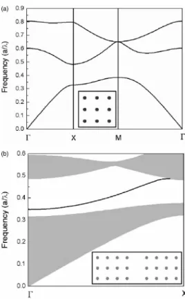
Figure 1共a兲 shows the PC structure 共the inset兲 that is under study as well as its band structure. The PC consists of a two-dimensional 共2D兲 square lattice of alumina rods in air. The refractive index of the alumina rods is 3.1. The lattice constant is a = 11 mm, and the radius of the rods is
r = 1.575 mm. This PC has a band gap for transverse
mag-netic polarization 共with a magnetic field perpendicular to the axis of the rods兲 in the frequency range of 共0.376–0.482兲a/, where is the wavelength in free space.
a兲Electronic mail: [email protected]
FIG. 1. 共a兲 Band structure of the 2D photonic crystal. The inset shows the PC structure with a square lattice. The black circles represent the dielectric rods共with refractive index of 3.1兲 placed in air. 共b兲 The projected band structure of the PC waveguide, which is formed by removing one column of rods from the PC, as shown in the inset. The grey regions are the projected pass bands, while the solid line is the dispersion curve of PC waveguide mode.
APPLIED PHYSICS LETTERS 91, 121105共2007兲
This frequency range corresponds to 10.26– 13.15 GHz for our experimental structure. Figure1共b兲shows the dispersion curve for the PC waveguide in the first band gap. After one row of rods is removed, a PC waveguide can be formed, as shown in the inset of Fig.1共b兲.
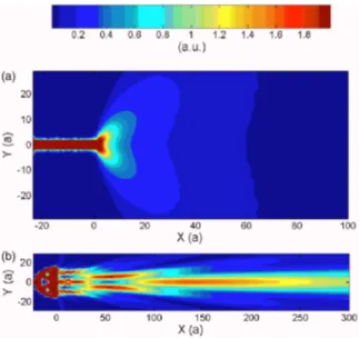
Figure 2共a兲 shows a PC structure with a waveguide opened directly on the surface, which will be used as a ref-erence for beaming measurements. Figure 2共b兲 shows the designed PC structure for the purpose of directional beam-ing. It can be seen intuitively from Fig. 2共b兲 that when a beam of an em wave propagates from the left to the right, it will be split into 16 beams when they reach the output ports. As all of the 16 beams propagate the same length, they will have the same phase when they arrive at the output ports. Consequently, these waves are expected to form a good directional emission. To study this possible phenomenon, we carry out 2D finite-difference time-domain16 共FDTD兲 simulations for the structures shown in Fig. 2, with the perfect matched layers17 which is applied as absorption boundaries. In the simulations, the frequency is chosen to be f = 0.417a / 共11.36 GHz兲, which represents about the middle of the PC waveguide mode band, as shown in Fig.1共b兲. The theoretical intensity distribution of the mag-netic field for the PC waveguide structure is shown in Fig. 3共a兲. As can be seen from the figure, the em wave is diffracted into a wide angle just as expected. Figure 3共b兲 shows the simulation results for the multi-beam structure 关depicted in Fig.2共b兲兴. It can be clearly seen that the emitted em wave possesses exceptional directivity.
In order to validate our simulation results, we conducted experiments in the microwave regime. In our experiments, an HP-8510C network analyzer was used to excite a horn antenna in order to obtain an incident em field.12 Another horn antenna connected to the same network analyzer was used to receive and measure the em power that was emitted from the output ports of the PC structure. The length of the alumina rods used in our experiment was 15 cm, which is at least five times longer than the em wavelengths used in the present study. This condition makes the constructed PC structure a good approximation to the 2D structure used in the simulations.
In order to clarify quantitatively the performance of our structure for directional emission, we calculated the far field
pattern for the structure shown in Fig.2共b兲 at the frequency
f = 0.417a /, which corresponds to the intensity distribution
of Fig.3共b兲. In the calculation of far field pattern, we applied near to far field transformation through Kirchoff’s integral. The inset of Fig. 4 shows the calculated far field radiation pattern result with a full width at half maximum共FWHM兲 of 4.1°. It can be seen clearly that most of the emitted energy remains within the main emission lobe, while the side lobes are effectively suppressed. These characteristics of the far field pattern are further confirmed by our experimental re-sults. In the measurement of the far field pattern, we used a horn antenna to scan a semicircle with radius R = 1.8 m from the center of exit face of the PC structure. Figure4shows the measured radiation pattern with a FWHM of 4.8°, which is in good agreement with the calculated results.
Most of the PC based beaming structures depends on grating structures. However, this results in a narrow operat-ing bandwidth.3,7,8 As described earlier, our structure uses only PC line-defect waveguides for splitting and then we combine these beams to achieve highly directional radiation. Therefore, it is expected that our structure should have a
FIG. 2.共a兲 Photonic crystal structure where the output port of waveguide is opened directly on the PC surface.共b兲 The proposed structure where a single waveguide port is split into 16 output ports.
FIG. 3.共Color online兲 共a兲 Intensity distributions of the electric field for the line defect structure shown in Fig.2共a兲.共b兲 The intensity distributions of the electric field for the multiple-output structure shown in Fig.2共b兲. Both simu-lations were done at the frequency f = 0.417a / 共11.36 GHz兲, and the X and
Y axes are scaled in the PC lattice constant a.
FIG. 4. 共Color online兲 Comparison of calculated and measured far field radiation patterns 共partial兲 for the designed structure at the frequency
f = 0.417a / 共11.36 GHz兲. The inset is the full calculated pattern for the
same structure and frequency.
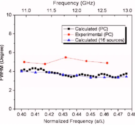
wider bandwidth when compared to the grating based PC beaming structures. In order to demonstrate this characteris-tic, we calculated and measured the far-field patterns for the frequencies within a wide bandwidth. Although the PC waveguide has a working frequency band within 0.376– 0.482a /, the group velocity of the waveguide mode be-comes increasingly slow near the band edges. The slow group velocity makes the incident wave rather difficult to couple into the input port of the PC waveguide. Accordingly, we focused our calculation and experimental study in the frequency range of 0.4– 0.476a /.
Figure 5 shows the calculated and measured FWHM data of the far field patterns for the PC structure shown in Fig.2共b兲. From the calculated data shown in Fig.5, it can be seen clearly that the FWHM remains at a rather low level 共less than 5°兲 within the whole frequency range of interest. This characteristic is further validated by our experimental results shown in Fig. 5. The measured FWHM results are slightly larger than the calculated ones, which might be par-tially due to the imperfections in the constructed structure, e.g., the slight randomness in the lattice constant, and the radii of the dielectric rods. Besides, the physical width of the horn antenna and some uncertainty共±2°兲 in its exact orien-tation can also affect the accuracy of the measurement. Nevertheless, our experimental results are in quite good agreement with the simulation results, which confirms that the PC based beaming structure that we present here works within a broad bandwidth. Furthermore, to gain additional insight for the underlying mechanism that yields the beaming phenomenon, we also did a FDTD simulation with barely 16 coherent point sources placed at the centers of the 16 output channels of the PC structure, but without the PC structure. The FWHM of the emission beam from 16 coherent point sources are also plotted in Fig.5. By comparing the results of 16 point sources and the PC structure with 16 output chan-nels, it is reasonable to say that the 16 output channels of the PC structure really serve like 16 coherent point sources. Conclusively, we can say that each output channel of the PC structure acts as a secondary source, and the superposition of these many small coherent channels is equivalent to a wide channel which would produce a collimated beam.
Besides the beaming structure with 16 output ports 关Fig.2共b兲兴, we also studied PC beaming structures with eight
and four output ports. The details of these results are not shown here because of space limitations. However, from the results that we obtained for the structures with eight and four ports, it is very clear that the directivity of the emitted beam is inversely proportional to the number of ports. This pro-vides a predictable performance for our proposed design. We also like to note that no optimization was applied for our beaming structure. Some special structures can be added to the present structure in order to enhance the efficiency of the beam bending,18beam splitting,19and coupling of the output ports to free space.20
Very recently, we noticed a report21 showing that a beaming phenomenon could appear in a structure that uti-lizes only two adjacent PC waveguide channels. The output field is analogous to a two-point-source interference pattern. The underlying mechanism is somewhat similar to our present design. Considering this type of beaming phenom-ena, both the number of channels and the proximity between the channels can affect the quality of the beaming effect. The optimal parameters might depend on the choice of the work-ing frequencies.
In conclusion, we experimentally and numerically achieved highly directional emission from a photonic crystal structure. When compared to gratinglike beaming structures, our PC beaming structure operates over a wider bandwidth. Our design principle can be easily generalized to other types of PC structures. This design can be used in photonic crystal lasers and in other applications to achieve highly directional emission.
This work is supported by the European Union under the projects EU-NoE-METAMORPHOSE, EU-NoE-PHORE-MOST, and TUBITAK, under Project Nos. 104E090, 105E066, 105A005, and 106A017. One of the authors共E.O.兲 also acknowledges partial support from the Turkish Academy of Sciences.
1H. J. Lezec, A. Degiron, B. Devaux, R. A. Linke, L. Martin-Moreno, F. J.
Garcia-Vidal, and T. W. Ebbesen, Science 297, 820共2002兲.
2P. Kramper, M. Agio, C. M. Soukoulis, A. Birner, F. Müller, R. B.
Wehr-spohn, U. Gösele, and V. Sandoghdar, Phys. Rev. Lett. 92, 113903共2004兲.
3E. Moreno, F. J. García-Vidal, and L. Martín-Moreno, Phys. Rev. B 69,
121402共R兲 共2004兲.
4J. D. Joannopoulos, R. D. Meade, and J. N. Winn, Photonic Crystals: Molding the Flow of Light共Princeton University Press, Princeton, 1995兲,
Vol. 1, pp. 94–104.
5E. Ozbay and B. Temelkuran, Appl. Phys. Lett. 69, 743共1996兲. 6B. Temelkuran, E. Ozbay, J. P. Kavanaugh, G. Tuttle, and K. M. Ho, B.
Temelkuran, Appl. Phys. Lett. 72, 2376共1998兲.
7I. Bulu, H. Caglayan, and E. Ozbay, Opt. Lett. 30, 3078共2005兲. 8S. K. Morrison and Y. S. Kivshar, Appl. Phys. Lett. 86, 081110共2005兲. 9D. Tang, L. Chen, and W. Ding, Appl. Phys. Lett. 89, 131120共2006兲. 10C.-C. Chen, T. Pertsch, R. Iliew, F. Lederer, and A. Tunnermann, Opt.
Express 14, 2423共2006兲.
11Z. H. Zhu, W. M. Ye, J. R. Ji, X. D. Yuan, and C. Zen, Appl. Phys. B:
Lasers Opt. 86, 327共2007兲.
12I. Bulu, H. Caglayan, and E. Ozbay, Appl. Phys. Lett. 83, 3263共2003兲. 13H. Caglayan, I. Bulu, and E. Ozbay, Opt. Express 13, 7645共2005兲. 14A. Mekis, J. C. Chen, I. Kurland, S. Fan, P. R. Villeneuve, and J. D.
Joannopoulos, Phys. Rev. Lett. 77, 3787共1996兲.
15M. Bayindir, E. Ozbay, B. Temelkuran, M. M. Sigalas, C. M. Soukoulis,
R. Biswas, and K. M. Ho, Phys. Rev. B 63, 081107共2001兲.
16K. Yee, IEEE Trans. Antennas Propag. 14, 302共1966兲. 17J.-P. Berenger, J. Comput. Phys. 114, 185共1966兲.
18J. Moosburger, M. Kamp, A. Forchel, S. Olivier, H. Benisty, C. Weisbuch,
and U. Oesterle, Appl. Phys. Lett. 79, 3579共2001兲.
19J. S. Jensen and O. Sigmund, J. Opt. Soc. Am. B 22, 1191共2005兲. 20B. Momeni and A. Adibi, Appl. Phys. Lett. 87, 171104共2005兲. 21Y. Zhang, Y. Zhang, and B. Li, Opt. Express 15, 9281共2007兲.
FIG. 5. 共Color online兲 FWHMs of the calculated and measured radiation patterns for the structure shown in Fig.2共b兲within the frequency range of 共0.4–0.476兲a/. The FWHM data of the radiation patterns for 16 coherent point sources are also shown for comparison.