Resonant cavity enhanced detectors embedded in photonic crystals
B. Temelkuran, E. Ozbay, J. P. Kavanaugh, G. Tuttle, and K. M. Ho
Citation: Appl. Phys. Lett. 72, 2376 (1998); doi: 10.1063/1.121361 View online: http://dx.doi.org/10.1063/1.121361
View Table of Contents: http://apl.aip.org/resource/1/APPLAB/v72/i19
Published by the American Institute of Physics.
Additional information on Appl. Phys. Lett.
Journal Homepage: http://apl.aip.org/
Journal Information: http://apl.aip.org/about/about_the_journal
Top downloads: http://apl.aip.org/features/most_downloaded
Information for Authors: http://apl.aip.org/authors
Resonant cavity enhanced detectors embedded in photonic crystals
B. Temelkurana) and E. Ozbay
Department of Physics, Bilkent University, Bilkent, Ankara, 06533 Turkey
J. P. Kavanaugh, G. Tuttle, and K. M. Ho
Ames Laboratory and Microelectronics Research Center, Iowa State University, Ames, Iowa 50011 ~Received 11 August 1997; accepted for publication 11 March 1998!
We report a resonant cavity enhanced ~RCE! detector built around a three-dimensional photonic band gap crystal. The RCE detector was built by placing a monopole antenna within the localized modes of planar and boxlike defect structures. The enhanced electric field around these defect structures were then measured by a microwave detector and a network analyzer. We measured a power enhancement factor of 3450 for planar cavity structures. A Fabry–Perot cavity model was used to understand and predict resonant cavity enhancement in this structure. The tuning bandwidth of the RCE detector extends from 10.5 to 12.8 GHz, which corresponds to the full photonic band gap by the crystal. These RCE detectors have increased sensitivity and efficiency when compared to conventional detectors, and can be used for various applications. © 1998 American Institute of
Physics. @S0003-6951~98!02219-0#
There is a great deal of current interest for the possibility of creating three-dimensional photonic crystals in which no electromagnetic~EM! wave propagation is possible for cer-tain frequencies.1–4 These crystals, built at various dimen-sions with different techniques,5,6 offer a wide range of ap-plications in a spectrum ranging from microwave, to optical frequencies.7–10Recently, Ho et al. have proposed and dem-onstrated a three-dimensional photonic crystal based on stacked dielectric rods, which can be fabricated at smaller scales by conventional methods.11–13 Defects or cavities around the same geometry can also be built by means of adding or removing rods from the so called layer-by-layer photonic crystals.14 The electrical fields in such cavities are usually enhanced,15 and by placing active devices in such cavities, one can make the device benefit from the wave-length selectivity and the large enhancement of the resonant EM field within the cavity. This effect has already been used in optoelectronics to achieve novel devices such as resonant cavity enhanced ~RCE! photodetectors and light emitting diodes.15 In this letter, we demonstrate the RCE effect by placing microwave detectors within the localized modes of photonic crystal defect structures.
In our experiments, we used a layer-by-layer dielectric photonic crystal designed to have three-dimensional band gap with a midgap frequency around 12 GHz. The layer-by-layer structure was constructed by using square-shaped alu-mina rods (0.32 cm30.32 cm315.25 cm). The photonic crystal has a center to center separation of 1.12 cm, corre-sponding to a dielectric filling ratio of;0.29. We used the output port of a microwave network analyzer and a standard gain horn to obtain EM waves. Defect structures built around the crystal were tested by putting them in the beam path of the EM waves propagating along the stacking direction. A square law microwave detector was placed inside the defect volume of the photonic crystal, along with a monopole an-tenna. The monopole antenna was kept parallel to the
polar-ization vector e of the incident EM wave in all measure-ments. The dc voltage on the microwave detector was used to measure the power of the EM field within the cavity. We also measured the enhanced field by feeding the output of the monopole antenna into the input port of the network ana-lyzer. The monopole antenna was constructed by removing the shield around one end of a microwave coaxial cable. The exposed center conductor which also acted as the receiver, was 2 mm long. The calibrated enhancement measurements were performed in the following manner. We first measured the enhanced EM field by the probe inside the cavity. While keeping the position of the probe fixed, we removed the crys-tal and repeated the same measurement. This single pass ab-sorption data of the probe was then used for calibration of the first measurement.
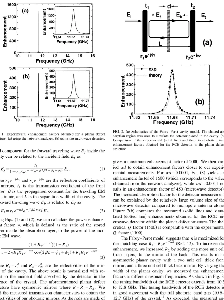
We first investigated a planar defect structure which was built around a 16 layer photonic crystal. The planar defect was obtained by separating the eighth and ninth layers of the structure.16 This resulted in a planar air gap between two photonic mirrors, each formed of an eight-layer crystal. Fig-ure 1~a! shows the enhancement characteristics of a planar defect structure with a separation width of 8.5 mm. The mea-surement was done by the network analyzer and the fre-quency was chosen to cover the photonic band gap of our crystal. We observed a power enhancement factor of 1600 at a defect frequency of 11.68 GHz. The Q factor~quality fac-tor!, defined as the center frequency divided by the full width at half maximum, was measured to be 900. We then mea-sured the enhancement characteristics of the same defect structure @Fig. 1~b!#, with a microwave detector, inserted in-side the same cavity. An enhancement factor of 450 along with a Q factor of 1100, were observed at the same defect frequency.
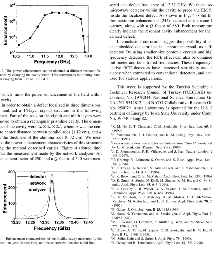
The discrepancy between two measured enhancement factors can be explained by modeling our structure as a Fabry–Perot cavity15 @Fig. 2~a!#. The probe we used in our experiments was simulated by an absorption region of thick-ness d, with a relative absorption coefficienta. The electric
a!Electronic mail: [email protected]
APPLIED PHYSICS LETTERS VOLUME 72, NUMBER 19 11 MAY 1998
2376
0003-6951/98/72(19)/2376/3/$15.00 © 1998 American Institute of Physics
field component for the forward traveling wave Efinside the cavity can be related to the incident field Eias
Ef5
t1
12r1r2e2ade2 j~2bL1f11f2!
Ei, ~1!
where r1e2 jf1 and r2e2 jf2 are the reflection coefficients of
the mirrors, t1 is the transmission coefficient of the front
mirror, b is the propagation constant for the traveling EM wave in air, and L is the separation width of the cavity. The backward traveling wave Eb is related to Ef as
Eb5r2e2ade2 j~bL1f2!Ef. ~2!
Using Eqs.~1! and ~2!, we can calculate the power enhance-ment factor h, which is defined as the ratio of the stored power inside the absorption layer, to the power of the inci-dent EM wave,
h5 ~11R2e2ad!~12R1!
122
A
R1R2e2ad cos~2bL1f11f2!1R1R2e22ad, ~3! where R15r12 and R25r22, are the reflectivities of the mir-rors of the cavity. The above result is normalized with re-spect to the incident field absorbed by the detector in the absence of the crystal. The aforementioned planar defect structure have symmetric mirrors where R5R15R2. We used the measured transmission characteristics to obtain the reflectivities of our photonic mirrors. As the rods are made of high quality alumina with a very low absorption coefficient, the absorption in the crystal can be neglected.16At the defect frequency, the transmission of an eight-layer crystal was 30 dB below the incident EM wave. The reflectivity of the pho-tonic mirrors was then obtained as R512T50.999. The ideal case which maximizeshcorresponds toad50, which
gives a maximum enhancement factor of 2000. We then var-ied ad to obtain enhancement factors closer to our
experi-mental measurements. For ad50.0001, Eq. ~3! yields an
enhancement factor of 1600~which corresponds to the value obtained from the network analyzer!, while ad50.0011
re-sults in an enhancement factor of 450 ~microwave detector!. The increased absorption factor for the detector measurement can be explained by the relatively large volume size of the microwave detector compared to monopole antenna alone. Figure 2~b! compares the measured ~solid line! and simu-lated ~dotted line! enhancements obtained for the RCE mi-crowave detector within the planar defect structure. The the-oretical Q factor~1500! is comparable with the experimental
Q factor~1100!.
The Fabry–Perot model suggests thathis maximized for the matching case R15R2e22ad ~Ref. 15!. To increase the
enhancement, we increased R2by adding one more unit cell
~four layers! to the mirror at the back. This results in an asymmetric planar cavity with a two unit cell thick front mirror, and a three unit cell thick back mirror. By varying the width of the planar cavity, we measured the enhancement factors at different resonant frequencies. As shown in Fig. 3, the tuning bandwidth of the RCE detector extends from 10.5 to 12.8 GHz. This tuning bandwidth of the RCE detector is in good agreement with the full photonic band gap ~10.6– 12.7 GHz! of the crystal.11 As expected, the measured en-hancement factors are relatively higher when compared with the symmetrical defect case. The maximum enhancement was measured to be 3450 at a defect frequency of 11.75 GHz. The theory predicted enhancement factors around 5500, which is higher than the measured values. The discrep-ancy can be explained by the finite size of the photonic
crys-FIG. 2. ~a! Schematics of the Fabry–Perot cavity model. The shaded ab-sorption region was used to simulate the detector placed in the cavity.~b! Comparison of the experimental ~solid line! and theoretical ~dotted line! enhancement factors obtained for the RCE detector in the planar defect structure.
FIG. 1. Experimental enhancement factors obtained for a planar defect structure:~a! using the network analyzer; ~b! using the microwave detector.
2377
Appl. Phys. Lett., Vol. 72, No. 19, 11 May 1998 Temelkuranet al.
tal, which limits the power enhancement of the field within the cavity.
In order to obtain a defect localized in three dimensions, we modified a 16-layer crystal structure in the following manner. Part of the rods on the eighth and ninth layers were removed to obtain a rectangular prismlike cavity. The dimen-sions of the cavity were 4a34a32d, where a was the cen-ter to cencen-ter distance between parallel rods~1.12 cm!, and d was the thickness of the alumina rods ~0.32 cm!. We mea-sured the power enhancement characteristics of this structure using the method described earlier. Figure 4 ~dotted line! shows the measurement made by the network analyzer. An enhancement factor of 290, and a Q factor of 540 were
mea-sured at a defect frequency of 12.32 GHz. We then used a microwave detector within the cavity to probe the EM field inside the localized defect. As shown in Fig. 4 ~solid line!, the maximum enhancement ~245! occurred at the same fre-quency, along with a Q factor of 680. Both measurements clearly indicate the resonant cavity enhancement for the lo-calized defect.
In conclusion, our results suggest the possibility of using an embedded detector inside a photonic crystal, as a RCE detector. By using smaller size photonic crystals and higher frequency detectors, the RCE effect can also be obtained at millimeter and far-infrared frequencies. These frequency se-lective RCE detectors have increased sensitivity and effi-ciency when compared to conventional detectors, and can be used for various applications.
This work is supported by the Turkish Scientific and Technical Research Council of Turkey ~TU¨BI˙TAK! under Contract No. 197E044, National Science Foundation Grant No. INT-9512812, and NATO-Collaborative Research Grant No. 950079. Ames Laboratory is operated for the U.S. De-partment of Energy by Iowa State University under Contract No. W-7405-Eng-82.
1K. M. Ho, C. T. Chan, and C. M. Soukoulis, Phys. Rev. Lett. 65, 3152 ~1990!.
2
E. Yablonovitch, T. J. Gmitter, and K. M. Leung, Phys. Rev. Lett. 67, 2295~1991!.
3For a recent review, see articles in Photonic Band Gap Materials, edited
by C. M. Soukoulis~Plenum, New York, 1996!.
4J. D. Joannopoulos, P. R. Villeneuve, and S. Fan, Nature~London! 386,
143~1997!.
5U. Gruning, V. Lehmann, S. Ottow, and K. Bush, Appl. Phys. Lett. 68,
747~1996!.
6C. C. Cheng, A. Scherer, V. Arbet-Engels, and E. Yablonovitch, J. Vac.
Sci. Technol. B 14, 4110~1996!.
7
E. R. Brown and O. B. McMahon, Appl. Phys. Lett. 68, 1300~1996!.
8D. R. Smith, S. Shultz, N. Kroll, M. Sigalas, K. M. Ho, and C. M.
Souk-oulis, Appl. Phys. Lett. 65, 645~1994!.
9P. L. Gourley, J. R. Wendt, G. A. Vawter, T. M. Brennan, and B. E.
Hammons, Appl. Phys. Lett. 6, 687~1994!.
10
K. A. McIntosh, L. J. Mahoney, K. M. Molvar, O. B. McMahon, S. Verghese, M. Rothschild, and E. R. Brown, Appl. Phys. Lett. 70, 2973
~1997!.
11E. Ozbay, J. Opt. Soc. Am. B 13, 1945~1996!. 12
S. Noda, N. Yamamoto, and A. Sasaki, Jpn. J. Appl. Phys., Part 2 35, L909~1996!.
13M. C. Wanke, O. Lehmann, K. Muller, Q. Wen, and M. Stuke, Science
275, 1284~1997!.
14
E. Ozbay, G. Tuttle, M. Sigalas, C. M. Soukoulis, and K. M. Ho, Phys. Rev. B 51, 13 961~1995!.
15M. Selim Unlu and S. Strite, J. Appl. Phys. 78,~1995!. 16E. Ozbay and B. Temelkuran, Appl. Phys. Lett. 69, 743~1996!.
FIG. 3. The power enhancement can be obtained at different resonant fre-quencies by changing the cavity width. This corresponds to a tuning band-width ranging from 10.5 to 12.8 GHz.
FIG. 4. Enhancement characteristics of the boxlike cavity measured by the network analyzer~dotted line!, and the microwave detector ~solid line!.
2378 Appl. Phys. Lett., Vol. 72, No. 19, 11 May 1998 Temelkuranet al.