Controlling Laser-induced Self-organized Patterns via Engineered Defects
E. Ergecen1, ¨O. Yavuz2, O. Tokel2, I. Pavlov3, A. Rızao˘glu2, F. ¨O. Ilday2,3
1Department of Electrical and Electronics Engineering, Middle East Technical University, Ankara, Turkey 2Department of Electrical and Electronics Engineering, Bilkent University, Ankara, Turkey
3Department of Physics, Bilkent University, Ankara, Turkey
Nanoscale periodic surface structures are of paramount importance in material science [1]. The recently demonstrated Nonlinear Laser Lithography (NLL) technique allows creating nanostructure arrays over indefinitely large surfaces with remarkable periodicity, not attainable by conventional laser induced periodic surface structure (LIPSS) methods [2]. Using NLL with linearly polarized femtosecond pulses, nanolines parallel to polarization emerge from initial surface roughness, and propagate on the surface as the laser beam is scanned. Here, we demon-strate that the final surface patterns depend not only on the polarization, but also on the surface morphology, which is controllable by introducing artificial defects. We use line defects as a control parameter to select a surface tiling from a set of available ones.
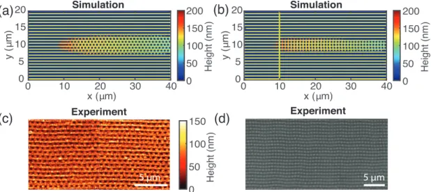
We simulate the evolution of periodic nanostructures using the mathematical model introduced in [2]. All surfaces used as a substrate here are first tiled with periodic horizontal nanolines, which are themselves created with NLL using horizontally polarized light. We then scan this substrate with a vertically polarized laser. As the beam propagates in positive x direction, a surface tiling emerges resembling a checkerboard pattern (Fig. 1(a)). This same initial substrate is modified to study the effect of a vertical line-defect, located at x = 10µm (Fig. 1(b)). The vertically polarized laser starts to the left of the vertical line-defect and is scanned in the positive x direction. We observe that a surface tiling emerges resembling a mesh pattern (Fig. 1(b)).
To compare with experiments, titanium (Ti) thin films (50 nm) were used. The experimental setup is detailed in [2]. We first scanned with a horizontally polarized laser to tile two surfaces with horizontal nanolines and used them as substrates. First substrate is scanned with a vertically polarized beam. The AFM image of this surface shows a checkerboard like pattern (Fig. 1(c)). The second substrate is modified with a vertical line, and then scanned with a vertically polarized laser (Fig 1(d)). We observed a mesh-like pattern as predicted by the simulations of Fig 1(b). The initial defect strongly influences the surface tiling, forcing the surface pattern to a mesh-like structure.
0 1 2 3 4 0 0.5 1 1.5 2 0 50 100 150 Simulation x (µm) 0 5 10 15 20 Height (nm ) 0 50 100 150 200 Experiment y (µ m) Simulation
(a)
5 µm Experiment 0 10 20 30 40 x (µm) 0 10 20 30 40 0 5 10 15 20 y (µ m) Height (nm ) 0 50 100 150 200(b)
(c)
(d)
Height (nm ) 5 µmFig. 1 (a) Surface pattern obtained by scanning the laser from (x,y) = (10,10) µm to (40,10) µm. (b) Surface pattern obtained by scanning the laser from (x,y) = (10,10)µm to (40,10) µm. (c) AFM image of the experiments corresponding to (a). (d) Optical microscopy image of the experiment corresponding to (b). The laser has a beam diameter of 10µm.
Although emergence of patterns in NLL is a stochastic process due to the intrinsic surface roughness, there is still a causal relationship between initial surface conditions and the final pattern. We exploit this relationship by manually introducing defects to influence the final 2D patterns. The intensity pattern induced by the additional defect (vertical line) is propagated during the laser scan. In conclusion, we demonstrated a novel method to control the evolution of surface structures formed by NLL. Initial surface defects along with polarization determines the final surface tiling. Notably, more complex periodic surface tilings, such as honeycomb lattices or quasicrystals might be obtained, and controlled by engineering the initial surface conditions.
References
[1] M. L. Brongersma, Y. Cui and S. Fan, “Light management for photovoltaics using high-index nanostructures,” Nature Mat.13, 451 (2014). [2] B. Oktem, I. Pavlov, S. Ilday, H. Kalaycioglu, A. Rybak, S. Yavas, M. Erdogan, and F. ¨O. Ilday, “Nonlinear laser lithography for indefinitely large-area nanostructuring with femtosecond pulses,” Nature Photon.7, 897 (2013).