Phys. Status Solidi RRL 10, No. 11, 792–796 (2016) / DOI 10.1002/pssr.201600204
www.pss-rapid.com
pss
CVD grown 2D MoS
2layers:
A photoluminescence and fluorescence
lifetime imaging study
Ayberk Özden*, 1 , Hüseyin Şar2 , Aydan Yeltik4 , Büşra Madenoğlu1 , Cem Sevik3 , Feridun Ay2 , and Nihan Kosku Perkgöz*, 2
1 Department of Materials Science and Engineering, Faculty of Engineering, Anadolu University, 26555 Eskisehir, Turkey 2 Department of Electrical and Electronics Engineering, Faculty of Engineering, Anadolu University, 26555 Eskisehir, Turkey 3 Department of Mechanical Engineering, Faculty of Engineering, Anadolu University, 26555 Eskisehir, Turkey
4 Department of Physics, UNAM Institute of Materials Science and Nanotechnology, Bilkent University, 06800 Ankara, Turkey
Received 30 June 2016, revised 24 August 2016, accepted 30 August 2016 Published online 5 September 2016
Keywords MoS2, two-dimensional materials, fluorescence lifetime imaging microscopy, photoluminescence, Raman spectroscopy,
chemical vapor deposition
* Corresponding authors: e-mail [email protected], Phone: +99 535 4172654; [email protected], *Phone: +0222 321 35 50, Ex: 6472
© 2016 WILEY-VCH Verlag GmbH & Co. KGaA, Weinheim
1 Introduction Understanding and control of the in-direct to in-direct electronic band gap transition of the transi-tion metal dichalcogenides (TMDCs) have attracted sig-nificant interest for the realization of atomically thin, flexi-ble and transparent optoelectronic devices [1]. With this motivation, various optoelectronic device configurations and light driven applications have been reported for 2D MoS2 (a prototypical material of the TMDCs family) where it is used as an active material in photodetectors, phototransistors, light-emitting diodes, solar cells and in
photocatalytic water splitting applications [2–4]. Moreover, lack of inversion symmetry and strong spin orbit coupling of these materials provides a possible mechanism of selec-tive photoexcitation of carriers with defined spin and val-ley indices leading to a new field of valval-leytronics [5]. In-teresting optical properties are not limited by the band gap transition and spin–orbit coupling effects but also include the wealth of exciton physics arising due to strong quan-tum confinement of excitons because of the larger Bohr radius of excitons (0.9 nm) than the thickness of the MoS2
In this letter, we report on the fluorescence lifetime imaging and accompanying photoluminescence properties of a chemi-cal vapour deposition (CVD) grown atomichemi-cally thin material, MoS2. µ-Raman, µ-photoluminescence (PL) and fluorescence
lifetime imaging microscopy (FLIM) are utilized to probe the fluorescence lifetime and photoluminescence properties of individual flakes of MoS2 films. Usage of these three
techniques allows identification of the grown layers, grain boundaries, structural defects and their relative effects on the PL and fluorescence lifetime spectra. Our investigation on in-dividual monolayer flakes reveals a clear increase of the fluo-rescence lifetime from 0.3 ns to 0.45 ns at the edges with re-spect to interior region. On the other hand, investigation of the film layer reveals quenching of PL intensity and lifetime at the grain boundaries. These results could be important for applications where the activity of edges is important such as in photocatalytic water splitting. Finally, it has been
strated that PL mapping and FLIM are viable techniques for the investigation of the grain-boundaries.
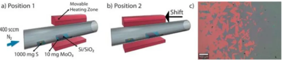
Figure 1 (a) Schematic configuration of the growth system and the initial furnace position (position 1). (b) Furnace position 2 is used when the growth temperature is reached. Furnace is shifted on the sulfur powder. (c) Resulting MoS2 film and large triangles at the
edge of the film. Note that scale bar is 100 µm.
monolayer (0.7 nm) [6, 7]. In addition, low quantum yield due to defective structure of CVD MoS2 can be increased from 0.6% to near unity (95%) by surface engineering [8].
Harnessing all these exotic phenomena for practical re-alization of devices, beyond the expensive and laboratory scale fabrication techniques such as electron beam lithog-raphy, requires growth of larger monolayer flakes, which is not possible using material synthesis techniques such as mechanical exfoliation. Moreover, to evaluate the device performance or fundamental properties including exciton lifetime, material homogeneity in terms of number of lay-ers, structural defects and compositional variation across the flake is of utmost importance. Therefore, in this letter, we use chemical vapour deposition as a primary growth method because of its potential (record high flake size achieved with CVD, larger than 300 µm [9]) to address the large area growth problem of 2D materials. To determine the material homogeneity, we use µ-Raman, µ-PL and Fluorescence Lifetime Imaging (FLIM). Although FLIM on the single and few layer mechanically exfoliated MoS2 decorated with CdSe quantum dots have already been per-formed by Prins et al. [10], we report the FLIM analysis of CVD grown bare MoS2 layers and flakes with intrinsic film features for the first time. We observe that CVD grown flakes and films exhibit heterogeneous features in both their photoluminescence and lifetime maps. We report fluorescence lifetimes of MoS2 in the range of 0.2 ns to 0.45 ns (error is ±0.1 ns) changing based on the micro-structure and position of the flakes (separate or merged in-to a film).
2 CVD growth In our study, a modified face-down approach similar to Wang et al. is used [11]. 1 g elemental S and 10 mg of MoO3 are used as precursors and realized reaction at 700 °C and at atmospheric pressure to grow MoS2 monolayers on the SiO2/Si substrate with a 285 nm thick amorphous SiO2 layer. The distance between S and MoO3 is fixed at 18 cm. Split furnace is used to have a mobile heater body to control the growth process carefully. When the growth temperature is reached, the furnace is shifted to the S precursor region to achieve sufficient flux of gaseous sulphur to prevent formation of molybdenum oxides. When all the sulphur evaporates, the upper furnace is lifted up for fast cooling to prevent secondary nucleation. When the furnace is used in static position (when it is not shifted toward sulphur and not lifted up), nanowall like growth of MoS2 structures with secondary oxide phases is
observed and reported in [12]. Optimisation of this particu-lar growth process will be reported elsewhere in detail. The schematic illustration of the furnace and furnace positions before and after reaching the growth temperature is dem-onstrated in Fig. 1(a) and (b) together with the resulting film formations containing up to 80 µm 2D triangular few layer flakes (Fig. 1(c)) that merge to form around 1 cm2 few layer MoS2 film. Subsequent characterisation of the flakes and film area is given in lifetime measurements, Section 3.
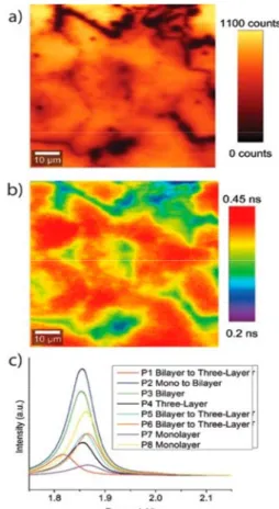
3 Lifetime measurements All measurements in this letter are performed at room temperature using Witec α-300 R µ-Raman system. Raman and PL measurements are performed with a continuous 532 nm excitation laser. Fluorescence lifetime measurements are performed using a 485 nm pulsed laser with 80 MHz repetition frequency and a resulting pulse width (FWHM) of 90 ps. Micro Photon Device’s PDM series photon counting detector module is used for the lifetime imaging measurements. 75 µm × 75 µm regions are selected for mapping. 375 × 375 data points (140625 total data points, meaning 200 nm pixel size) are scanned and resulting data proc-essed to get desired mapping images in Figs. 3 and 4. De-tails of the lifetime measurements and exponential decay fitting procedure can be found in the Supporting Informa-tion (Fig. S3 and S4). In the first part of these measuments, we performed a structural characterisation on a re-gion selected from the film zone. Confocal optical image of this zone is given in Fig. 2(a). Inspection of the confocal image provides additional layers and crack like boundaries (white lines) on a smooth surface. Splitting the furnace when the sulphur is completely finished might result in an additional stress on the film due to the thermal expansion mismatch between MoS2 and SiO2 underlayer. In addition to cracks (or wrinkles), thicker boundaries (greener con-trast in Fig. 2(a)) are observed as an extension of the cracks, suggesting that these cracks might behave as addi-tional nucleation sites. Therefore, this selected region pro-vides all the interesting points for PL and lifetime inspec-tion: layer properties, structural defects (cracks), secondary nucleation on these boundaries and regions demonstrating no defect in the confocal image. Point µ-Raman analysis of these zones is given in Fig. 2(b). E2g and A1g Raman peaks demonstrate the existence of MoS2 layers with changing layer number with respect to structure on the film. Raman inspection except for obvious thicker points (1, 4, 5
794 A. Özden et al.: CVD grown 2D MoS2 layers
Figure 2 (a) Confocal image of the film zone. Colored cross marks are the points where single point Raman measurement is per-formed. (b) Raman spectrum of point 1 (P1, red cross mark) to point 8 (yellow cross-mark). (c) A1g and E2g peak center differences and
corresponding layer number of the cross marked points. Horizontal dashed lines indicate specific values corresponding to number of layers in Refs. [13, 14].
and 6) indicates few layered MoS2. AFM measurements also point to the presence of few layered MoS2 as can be seen in Fig. S1, Supporting Information. In fact, our PL measurements reveal that these flakes are mostly in the form of few layers because we observe PL peak centers be-tween 1.82 and 1.86 eV, which is consistent with mono-layer and few mono-layer PL measurements of MoS2 [23, 24]. Number of layers of the selected points can be seen in Fig. 2(c). Raman spectra and its FWHM analysis can be found in Fig. S2 and Table S1 of the Supporting Information. Figure 3(a) demonstrates the total photoluminescence intensity map and Fig. 3(b) demonstrates the FLIM image of the same region introduced in Fig. 2. Figure 3(c) is the single point photoluminescence measurement of the points (coloured cross marks) given in Fig. 2 together with num-ber of layers indicated in the legend of Fig. 3(c). First of all, PL map reveals black lines (non-luminescent area) that we already mentioned as cracks (or wrinkles) in the confocal image (Fig. 2(a)). On the other hand, PL map also reveals secondary, very thin black lines, that separate hexagonal like grains which were not visible by confocal imaging. Total photoluminescence intensity map also reveals quenching of PL intensity at the boundaries (grain boundaries or cracks). Lifetime imaging is in line with the photoluminescence map that demonstrates a higher life-time in single layer regions (red zones) of the image (Fig. 3(b)) with respect to the defective sites (secondary layers and grain boundaries). Still, the measured fluores-cence lifetime is within the range of reported room tem-perature theoretical value of bright A exciton of monolayer MoS2, that is 0.27 ns [7]. PL peak centre of single point measurements shifts from 1.82 eV to 1.86 eV. As men-tioned earlier, cracks are the indication of possible stress. Profound local stress effect on the narrowing of the band gap (up to 90 meV with 2.5% tensile strain) is reported [15]. Therefore, in addition to thickness and composition, stress is not a negligible effect when considering PL shifts. Moreover, it has been demonstrated that CVD grown flakes possess also a compositional variance across the flakes possibly due to substrate position and concentration gradient along the quartz tube [11]. Variation of the PL in-tensities with respect to number of layers is also visible in
Fig. 3(a) and (c), suggesting different quantum yields in multi-layered structures.
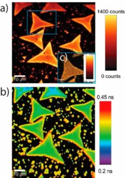
Herein, we also demonstrate lifetime imaging of sepa-rate flakes, which do not exhibit grain boundaries and other structural defects, such as stress related cracks. Fig-ure 4(a) and (b) shows the PL map and corresponding life-time imaging of the same region, respectively. Figure 4(c) (inset of Fig. 4(a)) is the map of Raman shift difference be-tween E2g and A1g peak centers of a selected flake. Delta values between 18 and 22 in Fig. 4(c) indicate a homogene-
Figure 3 (a) Total PL intensity map, (b) fluorescence lifetime map, (c) single point photoluminescence measurements. See Fig. 2 for the position of the points.
Figure 4 (a) PL mapping and (b) FLIM mapping of the separate flakes. (c) Map of difference between peak centers of E2g and A1g.
ous monolayer flake. Absence of such a graboundary in-teraction and a better pristine structure (no PL visible cracks or wrinkles) let us visualize the effect of the edges more clearly with respect to the interior part of the flake. Total PL intensity and lifetime of the edges are higher with respect to the interior or central regions (0.3 ns at interior and 0.45 ns at edges).
As demonstrated in Fig. 3(b), interaction of grains via a grain boundary quenches lifetime and decreases PL inten-sity, possibly by increasing the non-radiative decay chan-nels. As noted above, MoS2 flakes exhibit brighter PL and longer lifetimes at the edges of the flakes when compared to the interior parts of the standalone flakes (Fig. 4). In general, these results are attributed to the numerous fac-tors such as charge carrier density, defect density, strain, screening, band-bending, crystallinity and grain boundaries [16–20]. The possible reasons for the brighter PL with the longer decay lifetimes at the edges and lower PL with the shorter decay lifetimes at the interior points can be listed as the higher defect density, change in crystallinity and higher charge carrier density. For the further investigation of these findings, we performed PL measurements by using 532 nm CW laser and at various laser powers, and we obtained steady-state PL spectra from the interior region and the edges of the standalone flakes. As given in Fig. 5, we ob-served a significant red-shift in the PL spectra as the meas-urement point is moved from the lower PL point (interior region) to the higher PL point (edge region). Furthermore, this shift is significantly increasing with the increase in ex-citation power from 3 mW (10 meV) to 9 mW (19 meV). These observations, made under relatively high excitation powers, indicate that one possible reason for the weaker PL
Figure 5 Comparison of the PL spectra of edge and interior points at (a) 3 mW CW laser power with 10 meV PL shift and (b) 9 mW CW laser power with 19 meV PL shift.
and shorter lifetimes at the interior regions of the flakes could be a favored formation of trions and excitons to-gether leading to exciton–exciton annihilation or charge screening [21, 22]. Furthermore, in addition to exciton and trions, the formation of other species of excitons such as biexcitons and/or bound excitons could lead to increased contribution of radiative component at the edges.
4 Conclusion As a conclusion, we demonstrate the ef-fect of structural deef-fects, multiple layers, grain boundaries and edges on the optical properties of CVD grown MoS2 layers. The structural defects and additional layers change the optical properties. It is observed that the existence of grain boundaries both decrease the photoluminescence in-tensity and quench fluorescence lifetime, leaving defect free monolayers (inner of grains) with higher PL intensity and lifetime. Separate flakes on the other hand, exhibit an opposite behaviour, where edges have higher lifetime and photoluminescence intensity. This could be important for applications where edges play a key role, e.g. hydrogen evolution catalysts. Our results further demonstrate that even for perfect monolayer flakes or films there exists an optical heterogeneity, possibly due to stress or local com-positional change in flakes. Finally, usage of three imaging techniques (lifetime, Raman and PL) are demonstrated as a set of powerful tools to evaluate optical properties of a 2D material.
Supporting Information Additional supporting informa-tion may be found in the online version of this article at the pub-lisher’s website.
796 A. Özden et al.: CVD grown 2D MoS2 layers
Acknowledgements This work was supported by Anadolu University Research Projects no: BAP1407F335, BAP1505F271, BAP150BF228, and BAP1605F24. C.S. and A.Ö acknowledges support from Turkish Academy of Sciences (TUBA-GEBIP).
References
[1] K. F. Mak, C. Lee, J. Hone, J. Shan, and T. F. Heinz, Phys. Rev. Lett. 105, 136805 (2010).
[2] O. L. Sanchez, D. Lembke, M. Kayci, A. Radenovic, and A. Kis, Nature Nanotechnol. 8, 497 (2013).
[3] D. Li, R. Cheng, H. Zhou, C. Wang, A. Yin, Y. Chen, N. O. Weiss, Y. Huang, and X. Duan, Nature Commun. 6, 7509 (2015).
[4] H. Li, C. Tsai, A. L. Koh, L. Cai, A. W. Contryman, A. H. Fragapane, J. Zhao, H. S. Han, H. C. Manoharan, F. Abild-Pedersen, J. K. Nørskov, and X. Zheng, Nature Mater. 15, 45 (2016).
[5] D. Xiao, G. B. Liu, W. Feng, X. Xu, and W. Yao, Phys. Rev. Lett. 108, 196802 (2012).
[6] H. Shi, R. Yan, S. Bertolazz, J. Brivio, B. Gao, A. Kis, D. Jena, H. G. Xing, and L. Huang, ACS Nano. 7, 1072 (2013).
[7] M. Palummo, M. Bernard, and J. C. Grossman, Nano Lett.
15, 2794 (2015).
[8] M. Amani, D.-H. Lien, D. Kiriya, J. Xiao, A. Azcat, J. Noh, S. R. Madhvapathy, R. Addou, S. KC, M. Dubey, K. Cho, R. M. Wallace, S.-C. Lee, J.-H. He, J. W. Ager III, X. Zhang, E. Yablonovitch, and A. Javey, Science 350, 1065 (2015).
[9] Z. Lin, Y. Zhao, C. Zhou, R. Zhong, X. Wang, Y. H. Tsang, and Y. Chai, Sci. Rep. 5, 18596 (2015).
[10] F. Prins, A. J. Goodman, and W. A. Tisdale, Nano Lett.
14, 6087 (2014).
[11] S. Wang, Y. Rong, Y. Fan, M. Pacios, H. Bhaskaran, K. He, and J. H. Warner, Chem. Mater. 26, 6371 (2014).
[12] N. K. Perkgöz and M. Bay, Nano-Micro Lett. 8, 70 (2016).
[13] H. Li, Q. Zhang, C. C. R. Yap, B. K. Tay, T. H. T. Edwin, A. Olivier, and D. Baillargeat, Adv. Funct. Mater. 22, 1385 (2012).
[14] J. Jeon, S. K. Jang, S. M. Jeon, G. Yoo, Y. H. Jang, J. H. Park, and S. Lee, Nanoscale 7, 1688 (2015).
[15] A. Castellanos-Gomez, R. Roldá, E. Cappelluti, M. Bus-cema, F. Guinea, H. S. J. van der Zant, and G. A. Steele, Nano Lett. 13, 5361 (2013).
[16] Z. Liu, M. Amani, S. Najmaei, Q. Xu, X. Zou, W. Zhou, T. Yu, C. Qiu, A. G. Birdwell, F. J. Crowne, R. Vajtai, B. I. Yakobson, Z. Xia, M. Dubey, P. M. Ajayan, and J. Lou, Nature Commun. 5, 5246 (2014).
[17] J. Feng, X. Qian, C.-W. Huang, and J. Li, Nature Photon. 6, 865 (2012).
[18] S. Tongay, J. Suh, C. Ataca, W. Fan, A. Luce, J. S. Kang, J. Liu, C. Ko, R. Raghunathanan, J. Zhou, F. Ogletree, J. Li, J. C. Grossman, and J. Wua, Nano Lett. 13, 2831 (2013). [19] W. Bao, N. J. Borys, C. Ko, J. Suh, W. Fan, A. Thron,
Y. Zhang, A. Buyanin, J. Zhang, S. Cabrini, P. D. Ashby, A. Weber-Bargioni, S. Tongay, S. Aloni, D. F. Ogletree, J. Wu, M. B. Salmeron, and P. J. Schuck, Nature Commun.
6, 7993 (2015).
[20] A. M. V. D. Zande, P. Y. Huang, D. A. Chenet, T. C. Ber-kelbach, Y. You, G.-H. Lee, T. F. Heinz, D. R. Reichman, D. A. Muller, and J. C. Hone, Nature Mater. 12, 554 (2013). [21] K. F. Mak, K. He, C. Lee, G.-H. Lee, J. Hone, T. F. Heinz,
and J. Shan, Nature Mater. 12, 207 (2013).
[22] K. P. Dhakal, D. L. Duong, J. Lee, H. Nam, M. Kim, M. Kan, Y. H. Lee, and J. Kim, Nanoscale 6, 13028 (2014). [23] N. Scheuschner, O. Ochedowski, A.-M. Kaulitz, R. Gillen,
M. Schleberger, and J. Maultzsch, Phys. Rev. B 89, 125406 (2014).
[24] Y. Jung, J. Shen, and J. J. Cha, Nano Convergence 1, 1–18 (2014).