PHYSICS. CHEMISTRY AND APPLICATION OF NANOSTRUCTURES. 2009
ELECTRIC FIELD EFFECTS ON OPTICAL PROPERTIES OF SEMICONDUCTOR NANORODS
L. 1. GURINOVICH, A. A. LUTICH, A. P. STUPAK, S. Va. PRISLOPSKII
B.I. Stepanov Institute of Physics NASB. Nezavisimosti Ave. 68. 220072 Minsk. Belarus [email protected]
M. V. ARTEMYEV, E. K. RUSAKOV
Institute for Physico-Chemical Problems, Belarusian State University Leningradskaya I4, 220080 Minsk. Belarus
H. V. DEMIR
Department of Physics, Department of Electrical and Electronics Engineering Nanotechnology Research Center, Bilkent University
Bilkent, TR-06800 Ankara, Turkey
We studied electric field effects on optical properties ofCdSe/ZnS nanorods integrated in thin films sandwiched between transparent electrodes. It was demonstrated that P-polarized component of the photoluminescence of CdSelZnS nanorods is quenched stronger by external electric field than the S-polarized component. Quantum dots are more sensitive to external electric field than the nanorods. A mechanism of external electric field influence on the luminescence spectrum of semiconductor nanorods is discussed.
1. Introduction
It was previously demonstrated theoretically [1] and experimentally [2] that semiconductor quantum dots (QDs) show strong dependence of optical properties on an electric field. Chemically synthesized semiconductor nanorods also exhibit the electric field effects. For example, quantum-confined Stark effect and luminescence quenching of single nanorods were previously demonstrated [3-5]. Unlike QDs, the nanorods exhibit quantum confinement only in two dimensions. It is reasonable to assume that the electric field applied along a nanorod may result in the strong polarization dependence of photoluminescence (PL). In the present paper, we investigate the influence of an external electric field onto luminescent properties of chemically synthesized CdSe/ZnS nanorods.
2. Sample preparation
CdSe/ZnS core-shell nanorods ca. (dx!) 4x25 and 5x20 nm were synthesized according to the published procedures [6]. The polymeric polymethylmetacrylate
133
(PMMA) film with CdSe/ZnS nanorods was placed between two transparent ITO electrodes sealed with epoxy glue. The electric field influence on the nanorods PL was studied by applying a constant voltage between the transparent ITO electrodes. The PL spectra of S- and P-polarization were measured by a spectrofluorimeter "CM 2203 Solar".
3. Results
3.1. Electricjield effect on PL ojCdSe/ZnS nanorods
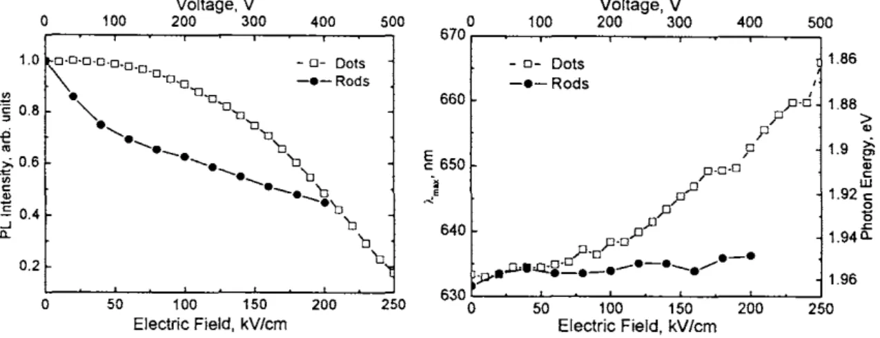
Fig. 1 shows PL intensity and PL peak position of CdSe/ZnS nanorods in PMMA film at different applied voltages in comparison with QDs with average size of 4 nm. ~ ~O.6 2 E 0.4 ...J 11. 0.2 Voltage, V Voltage, V 100 200 300 400 500 0 100 200 300 400 500 r----.~--r----r----._--_. 6 7 0 r - - - - r - - - - . -__ ~--~ __ --~ - 0- Dots -e-Rods 50 100 150 200 250 Electric Field, kVlcm - 0- Dots -.-Rods 660 p p 640 pod p 1.86 1.88 ~ 1.9 ~ " c w 1.92 c o (5 1.945: 1.96 630 0'----:5:':-0---:1..,OO,..--1-':-50:---2:-:'-OO.,--~250 Electric Field, kV/cm
Figure I. Relative PL intensity and PL peak wavelength (Amax) of CdSe/ZnS nanorods
(ca. 4x25 nm) film at different applied electric fields in comparison with quantum dots of average
size of4 nm.
The curves in Fig. 1 demonstrate the decrease of PL intensity (quenching) and the red shift of PL maximum with the voltage increased. At the values of electrical field strength E up to 105 V Icm the PL of nanorods is quenched more than PL of QDs. However, the wavelength shift of PL maximum with applied electric field for nanorods increases very weak. Evidently, due to the elongated shape of nanorods, the external electric field effect may differ for S- and P-polarized PL. This property is important for application of this material in optoelectronic nanodevices. To understand reasons of the electric field effect difference between QDs and nanorods, the mechanism of nanorodsPL quenching has to be studied. The quantum-confined Stark effect is probably not the single factor in force.
134
3.2. Polarization of CdSeJZnS nanorods photoluminescence
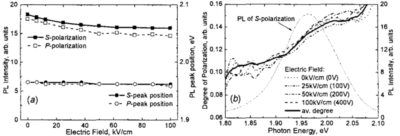
PL polarization of CdSe/ZnS nanorods (ca. 5x20 nm) at different electric fields was studied. The P-polarized component of the PL is quenched more efficiently than the S-component (Fig. 2a). Spectral positions of PL maxima for both components deviated weakly with voltage increased. The degree of polarization was calculated using the equation:
(I)
with Iii (h) being the components of emitted radiation with parallel (orthogonal) polarization with respect to the polarization of the excitation radiation. The average degree of polarization was calculated from the data of different experiments.
PL of nanorods is partially polarized and the degree of polarization is nearly field-independent. The difference of the polarization degree from left and right sides of PL band makes evident that PL spectrum has a complex structure (Fig.2b). 20 ".--_~_-~_-~_--,--,2.1
~~.--~.--.--.~~-
- "'0. - -0 • • • • ~S-pOlarizatiO~'" -0-'" -0. - -0-'" -0- --0 o '215 " €..
- 0- P-polarization c of10
~ 2.0~ (a) ~ 5 o-o~e~e~e~o-o-o-o~e-e-S-peak position
- 0- P-peak position L-.L.----'-~~~~----'-~J-11.9 o 20 40 60 SO 100 Electric Field, kV/cm Cl. ~
..
~ ~ c ~ 0.12 .~ ~ 0.10 o Q) ~o.os (b) o Electric Field: . OkV/cm (OV) •..•.. 25kV/cm (100V)· ···50kVlcm (200V) _ •• 100kVlcm (400V) -av.degree ., ... 0.06 0 1.S0 1.S5 1.90 1.95 2.00 2.05 2.10 Photon Energy, eVFigure 2. PL intensity and peak positions of S· and P·polarization (a) and average degree of PL
polarization (b) ofCdSelZnS nanorods ca. 5x20 nm vs electric field applied.
3.3. Electric field effect on absorption of CdSeJZnS nanorods
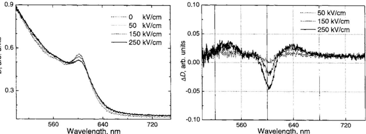
Fig. 3 displays the absorption spectra of CdSe/ZnS nanorods with average size of ca. 4x25 nm in the PMMA film at different applied voltage. The differential absorption spectra demonstrate the essential width and decrease in the first peak magnitude with the voltage increased. However, the quantum-confined Stark red shift [7,8] of the peak spectral position does not occur.
2 0.9 '--~----'---'---r---, . ···0 kV/cm 50 kV/cm -.--.-- 150 kV/cm 135 0 . 1 0 , - , - - - - r - - - , - - - , ... 50 kVfcm .---. 150 kV fcm -250kVfcm "§ 0.6 -250kV/cm 'c 2 :::> 0.3 c:i <l -0.05 -0.10 L - L - _ L - _ - ' - - _ - ' - - _ - ' - - _ - ' - - - - ' 560 640 720 560 640 720 Wavelength, nm Wavelength, nm
Figure 3. Absorption (D = 19 loll) and differential absorption (M) = D- D()v) spectra of CdSe/ZnS
nanorods ca. 4x25 nm versus electric field applied.
4. Conclusions
PL of CdSe/ZnS nanorods is partially polarized and the degree of polarization is nearly independent of external electric field. The P-polarized component of the PL is quenched more efficiently than the S-component. Spectral positions of PL maxima for both components have been deviated weakly with the voltage increased. The effect of sensitivity of PL properties of CdSe/ZnS nanorods with respect to electric field may find application in luminescent electromodulators.
Acknowledgement
This work is partially supported by PhOREMOST Network of Excellence and Belarusian-Turkish Joint Research Project (TOBiTAK-NASB).
References
1. S. Gaponenko, Optical Properties of Semiconductor Nanocrystals
(Cambridge University Press, 1998).
2. A. Lutich, S. Gaponenko, M. Artemyev, E. Ustinovich, 1. Soganci et aI., in: Physics, Chemistry, and Applications of Nanostructures, ed. by
V.E. Borisenko, S.V. Gaponenko, V.S. Gurin, (World Scientific, Singapore, 2007), p. 137.
3. E. Rothenberg, M.Kazes, E.Shaviv, U.Banin, Nano Lett. 5, 1581 (2005).
4. J. Muller, lM. Lupton, P.G. Lagoudakis et aI., Nano Lett. 5,2044 (2005).
5. R.M. Kraus, P.G. Lagoudakis et aI., Phys. Rev. Lett. 98,017401 (2007).
6. T. Mokari, U. Banin, Chern. Mater. 15,3955 (2003).
7. S.A. Empedocles, M.G. Bawendi, Science 278, 2114 (1997).