ESTIMATION OF RECEIVER SAMPLING CLOCK
TIMING IMPURITY IMPACT ON CHANNEL
ORTHOGONALITY IN OFDM BASED
COMMUNICATION SYSTEMS
a thesis
submitted to the department of electrical and
electronics engineering
and the institute of engineering and sciences
of bilkent university
in partial fulfillment of the requirements
for the degree of
master of science
By
H. Onur TANYER˙I
August 2009
I certify that I have read this thesis and that in my opinion it is fully adequate, in scope and in quality, as a thesis for the degree of Master of Science.
Dr. Tarık REYHAN(Co-Supervisor)
I certify that I have read this thesis and that in my opinion it is fully adequate, in scope and in quality, as a thesis for the degree of Master of Science.
Prof. Dr. Erdal ARIKAN(Co-Supervisor)
I certify that I have read this thesis and that in my opinion it is fully adequate, in scope and in quality, as a thesis for the degree of Master of Science.
Assist. Prof. Defne AKTAS¸
I certify that I have read this thesis and that in my opinion it is fully adequate, in scope and in quality, as a thesis for the degree of Master of Science.
Assist. Prof. F. ¨Omer ˙Ilday
ABSTRACT
ESTIMATION OF RECEIVER SAMPLING CLOCK
TIMING IMPURITY IMPACT ON CHANNEL
ORTHOGONALITY IN OFDM BASED
COMMUNICATION SYSTEMS
H. Onur TANYER˙I
M.S. in Electrical and Electronics Engineering
Co-Supervisor: Prof. Dr. Erdal ARIKAN
Co-Supervisor: Dr. Tarık REYHAN
August 2009
The growing need for high-speed wireless communication systems has led com-munication engineers to design and implement comcom-munication systems at higher frequencies where more bandwidth is available, use digital modulation schemes with more complex constellations and place carriers closer together with little guard-band in the pursuit of designing communication systems closer to the channel capacity. These new designs have placed tighter constraints on the per-formance of oscillators and timing devices of transceivers. In this work, the effects of timing clock jitter on the receiver Analog-to-Digital Converter (ADC) of Orthogonal Frequency Division Multiplexing (OFDM) based communication systems are examined and Inter-Carrier Interference (ICI) effects are quantified in order to prevent unnecessary over designs in OFDM ADC circuitry. In this respect, a simulation tool that synthesizes jitter processes with defined spec-tral characteristics is prepared. The generated jitter processes are utilized in an
sampling jitter. Using these two tools, ICI levels of certain OFDM systems are examined and guidelines for OFDM ADC circuitry design are proposed.
Keywords: Phase Noise, Phase Noise Synthesis, Jitter, ADC Sampling Jitter,
Orthogonal Frequency Division Multiplexing (OFDM), Inter-Carrier Interference (ICI)
¨
OZET
ALMAC
¸ ¨
ORNEKLEME ZAMANLAMA HATALARININ OFDM
HABERLES¸ME S˙ISTEMLER˙INDEK˙I KANAL
ORTOGONAL˙ITES˙INE ETK˙IS˙IN˙IN TAHM˙IN˙I
H. Onur TANYER˙I
Elektrik ve Elektronik M¨uhendisli¯gi B¨ol¨um¨u Y¨uksek Lisans
Ortak Tez Y¨oneticisi: Prof. Dr. Erdal ARIKAN
Ortak Tez Y¨oneticisi: Dr. Tarık REYHAN
Agustos 2009
Y¨uksek hızlı kablosuz haberle¸sme sistemlerine artan talep ve ihtiya¸c haberle¸sme m¨uhendislerini daha fazla bant geni¸sli˘ginin bulundu˘gu y¨uksek frekanslarda haberle¸sme sistemleri tasarlayıp yapmaya, daha karma¸sık mod¨ulasyon ¸semaları kullanmaya ve frekans ¸coklamalı sistemlerde bilgi barındıran ta¸sıyıcıların frekanslarını birbirlerine daha yakın koymaya zorlamı¸stır. Bu yeni tasarım gereksinimleri alma¸c ve g¨onderme¸clerdeki osilat¨or ve zamanlama elemanları ¨uzerine yeni performans kısıtlamaları getirmi¸stir. Bu ¸calı¸smada Ortogonal Frekans C¸ oklamalı (OFDM) temelli haberle¸sme sistemlerindeki alma¸cların Ana-log Dijital C¸ eviricilerinin (ADC) ¨ornekleme zamanlarındaki titre¸smelerin OFDM temelli haberle¸sme sistemlerine etkileri incelenmistir. Bu inceleme sayesinde bahsedilen bu etkilerin b¨uy¨ukl¨ukleri belirlenerek OFDM alma¸c devrelerinde yapılan a¸sırı sıkı tasarımlar engellenebilir. Bu etkilerin belirlenmesi i¸cin ¨oncelikle belirli tayf yo˘gunluk karakteristiklerine sahip ¨ornekleme zamanlaması titre¸sme sinyallerini sentezleyebilen bir program hazırlanmı¸stır. Bu programın ¸cıktı
sinyal-saatinde kullanılarak bu titre¸smelerin kanal ortogonalitesine olan etkileri ve yarattıkları Ta¸sıyıcılar Arası Enteferans (ICI) seviyeleri sim¨ulasyonlarla belir-lenmi¸stir. Belirlenen bu seviyeler temel alınarak OFDM alma¸c ADC tasarımında kullanılabilecek ¨oneriler sunulmu¸stur.
Anahtar Kelimeler: Faz g¨ur¨ult¨us¨u, Zamanlama titre¸smesi, Analog Dijital C¸ evirici, ¨ornekleme zamanı titre¸smesi, Ortogonal Frekans C¸ oklamalı Haberle¸sme Sistemleri (OFDM), Ta¸sıyıcılar Arası Enteferans (ICI)
ACKNOWLEDGMENTS
I would like to thank my father ˙Ibrahim TANYER˙I, my mother Erg¨ul TANYER˙I and my sister Ba¸sak TANYER˙I for supporting me all my life. Their presence is a blessing.
I would also like to thank all of my teachers and professors for enlightening me and helping me discover the beauty of engineering. I would especially like to thank Dr. Tarık REYHAN for bearing with me for the last three years and constantly teaching me through this time.
I would also like to thank my Co-supervisor Prof. Dr. Erdal ARIKAN for all of his efforts. Especially for helping me understand the methodology in scientific research.
Last, but not least, I would like to thank all of my friends Anıl BAYER, Ceyda BAYER, And S ¨UREKC˙IG˙IL, Barbaros S¸ERBETC¸ ˙I, Sıla KURAL and my colleagues at Biluzay that encouraged and helped me constantly.
Contents
1 Introduction 1
2 OFDM As a Bandwidth Efficient Communication System 7
2.1 OFDM . . . 7
2.2 OFDM Fundamentals . . . 8
2.3 OFDM Parameters . . . 20
3 Oscillator Fundamentals and Timing Impurities of Oscillators 22 3.1 Oscillator Fundamentals . . . 22
3.2 Phase Noise and Phase Noise Definition . . . 25
3.3 Phase Noise Models . . . 28
3.3.1 Oscillator Phase Noise Models . . . 30
3.4 Jitter and Phase Noise to Jitter Conversion . . . 34
4.1 The ICI Effects of Local Oscillator Phase Noise on OFDM
Com-munication Systems . . . 36
4.1.1 Mitigation From ICI Due to Local Oscillator Phase Noise . 39 4.2 The ICI Effect Due to The Timing Jitter on Receiver ADC . . . . 41
5 Simulations on Receiver ADC Timing Jitter ICI Effects 46 5.1 Generating Phase Noise With Certain Spectral Characteristics . . 47
5.2 Quantifying ICI Due to Timing Jitter on OFDM Receiver ADC . 51 5.3 Case Studies . . . 54
5.3.1 Case 1: IEEE 802.11a Communication System . . . 55
5.3.2 Case 2: IEEE 802.15.3a Communication System . . . 60
5.4 Minimum White Phase Noise in An Amplifier . . . 63
5.5 Discussion on Simulations and Design Guidelines . . . 65
5.6 Additional Factor Effecting ICI . . . 67
6 CONCLUSIONS 68 APPENDIX 73 A MATLAB Code For Quantifying ICI 73 A.0.1 Quatifying The ICI Due to Jitter Caused by Colored Jitter in A/D . . . 73
List of Figures
1.1 Zero-IF OFDM Transmitter Used in Simulations . . . 4
1.2 Zero-IF OFDM Receiver Used in Simulations . . . 4
2.1 Simple OFDM Transmitter Block Diagram . . . 9
2.2 Simple OFDM Receiver Block Diagram . . . 9
2.3 Sample Transmit and Receive Filters For an OFDM Communica-tion System . . . 12
2.4 OFDM Filters Created by IFFT Operation For an Eight Channel OFDM System(Frequency Domain) . . . 14
2.5 OFDM Filters Created by IFFT Operation For an Eight Channel OFDM System(Time Domain) . . . 15
2.6 Block Diagram of an OFDM Transmitter Using IFFT For Multi-Carrier Modulation . . . 15
2.7 Block Diagram of an OFDM Receiver Using FFT For Multi-Carrier Demodulation . . . 16
3.2 Output of an Ideal Oscillator . . . 26
3.3 Output of a Real Oscillator . . . 27
3.4 Sample Phase Noise Plot of an Vectron VCC6-QCD-250M000 Os-cillator [31] . . . 28
3.5 Injected Noise to Phase Noise Conversion Mechanism . . . 32
3.6 Illustration of Timing Jitter . . . 34
4.1 OFDM Transmitter Block Diagram Displaying the Transmit Local Oscillator Causing ICI . . . 37
4.2 OFDM Receiver Block Diagram Displaying the Receive Local Os-cillator Causing ICI . . . 37
4.3 Example for Spectral Phase Noise Estimation . . . 41
5.1 Sample Phase Noise Plot of an Vectron VCC6-QCD-250M000 Os-cillator [31] . . . 48
5.2 Synthesized White Phase Noise . . . 49
5.3 Phase Noise Power Spectral Density Created by a Random Walk with Step Strength 1fs and 400fs White Phase Noise on a 250 MHz Oscillator . . . 50
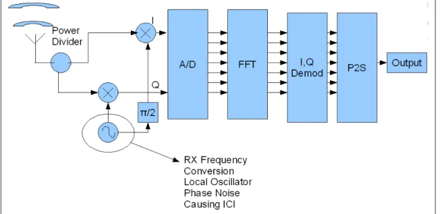
5.4 OFDM Receiver with Timing Jitter on ADC . . . 51
5.5 Plot Showing Interference to Carrier Power Ratios due to ICI and Intra Carrier Interference on a 4-QAM 10 MHz Bandwidth in an OFDM system with 64 Carriers having 100ps Random Walk Jitter 54
5.6 Phase Noise Power Spectral Density of Sample Oscillator 1 Used in IEEE 802.11a Simulations . . . 55
5.7 Interference to Signal Power Ratio created by Sampling Jitter on Sample Oscillator 1 . . . 56
5.8 Interference to Signal Power Ratio created by Sampling Jitter on Sample Oscillator That Only has 3ps Random Walk Jitter . . . . 57
5.9 Interference to Signal Power Ratio Created by Random Walk Sam-pling Jitter, Only Channel 10 is Used . . . 59
5.10 Interference to Signal Power Ratio Created by White Sampling Jitter, Only Channel 10 is Used . . . 59
5.11 Interference to Signal Power Ratio Created by Sampling White Jitter, Only Channel 1 is Used . . . 60
5.12 Sample 500MHz Oscillator 1 Used For Simulations of IEEE 802.15.3a UWB Communication System . . . 61
5.13 Interference to Signal Power Ratio Created by Timing Jitter Cre-ated Sample 500 MHz Oscillator 1 . . . 61
5.14 Sample 500MHz Oscillator 2 Used For Simulations of IEEE 802.15.3a UWB Communication System . . . 62
5.15 Interference to Signal Power Ratio Created by Timing Jitter Cre-ated Sample 500 MHz Oscillator 2 . . . 63
Chapter 1
Introduction
The electromagnetic spectrum is a very valuable and scarce resource. The ever increasing need for high-speed wireless communication systems has caused the electromagnetic spectrum to get crowded with information bearing carriers. This situation has forced communication engineers to design communication systems at higher frequencies where more bandwidth is available. Still, the availabil-ity of new frequency bands in the spectrum, if not protected by regulations, is destined to get crowded. This fact indicates the need to maximally utilize the electromagnetic spectrum. This can be done by designing bandwidth efficient wireless communication systems that can operate close to the channel capac-ity. This means, placing carriers close together in frequency division multiplexed systems and using complex digital modulation schemes in order to transmit at higher data rate using small bandwidths. By performing the actions mentioned above, one can make better use of the spectrum. These actions place some con-straints on certain parameters of communication systems. One set of concon-straints is placed on timing devices of wireless transceivers. Parameters like phase noise, jitter and stability that define the purity of oscillators are closely related to these constraints. These challenges in the design can be overcome by various expen-sive solutions with excesexpen-sive designs, such as using over qualified components
in the design, like unnecessarily stable oscillators with unnecessarily low phase noise performance. But the telecommunication market favors cheap, simple and lightweight(mobile) systems that consume less power.
In this work, Orthogonal Frequency Division Multiplexing (OFDM) based communication systems which are highly bandwidth efficient communication systems are investigated. OFDM is being increasingly used as standard digi-tal multi-carrier modulation method in various communication systems due to its bandwidth efficient nature and its robustness against multipath effects. The bandwidth efficient nature of OFDM comes from the fact that channel filtering (selection) is done by the orthogonality of the OFDM carriers. OFDM systems do not require guard-band. Furthermore, OFDM channels spectrally overlap in the frequency domain. This kind of spectral efficiency comes with its cost. OFDM communication systems are highly vulnerable to synchronization errors. This vulnerability results in stringent requirements for the timing elements of OFDM communication systems. The impact of these constraints should be quantified and converted into design specifications for efficient designs.
In this thesis, the focus is on the effects of receiver ADC sampling clock timing jitter on OFDM communications. In the thesis a perfect channel is assumed, only the timing jitter on the receiver sampling clock is considered as an impurity (i.e impurities like quantization noise, ADC aperture jitter are not included in the analysis). The amount of Inter-Carrier Interference (ICI) caused by timing jitter in OFDM receiver ADC’s is quantified for various OFDM communication systems. For this purpose jitter processes are modelled and generated. The generated processes are used in MATLAB simulations and ICI levels in OFDM carriers have been quantified for various OFDM communication systems. This
In Chapter 2, OFDM communication systems and the fundamental properties of OFDM are examined. The principles of OFDM communication systems are presented. OFDM parameters and OFDM parameters that are important for the analysis of receiver ADC sampling jitter effects are stated. Lastly, the effects of certain timing impurities on OFDM systems has been investigated.
In Chapter 3, oscillator fundamentals, oscillator parameters and timing impu-rities on oscillators are examined. Phase noise is studied in detail, because phase noise will be used extensively in the analysis. The definition of phase noise, the sources of phase noise, factors adding onto phase noise, ways of modelling phase noise, the relation between oscillator phase noise and timing jitter are presented.
In the Chapter 4 a summary of the previous studies performed on ICI created by local oscillator phase noise and ICI created by the timing jitter of the oscillator driving the receiver ADC of the OFDM receiver is presented. First, the previous work on the ICI effects caused by the phase noise of local oscillators performing frequency conversions are reviewed. Also, the techniques that are proposed for eliminating these effects are reviewed. Finally, the previous work on ICI caused by receiver ADC sampling clock timing jitter in OFDM systems is presented.
In Chapter 5, the analysis and studies performed on the ICI effects caused by OFDM receiver ADC sampling clock jitter are presented. First, the simulation tool that is prepared to generate jitter processes with defined phase noise spec-trum is presented. Then, the model that is used for simulating the ICI effects created due to jitter is presented.
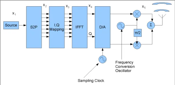
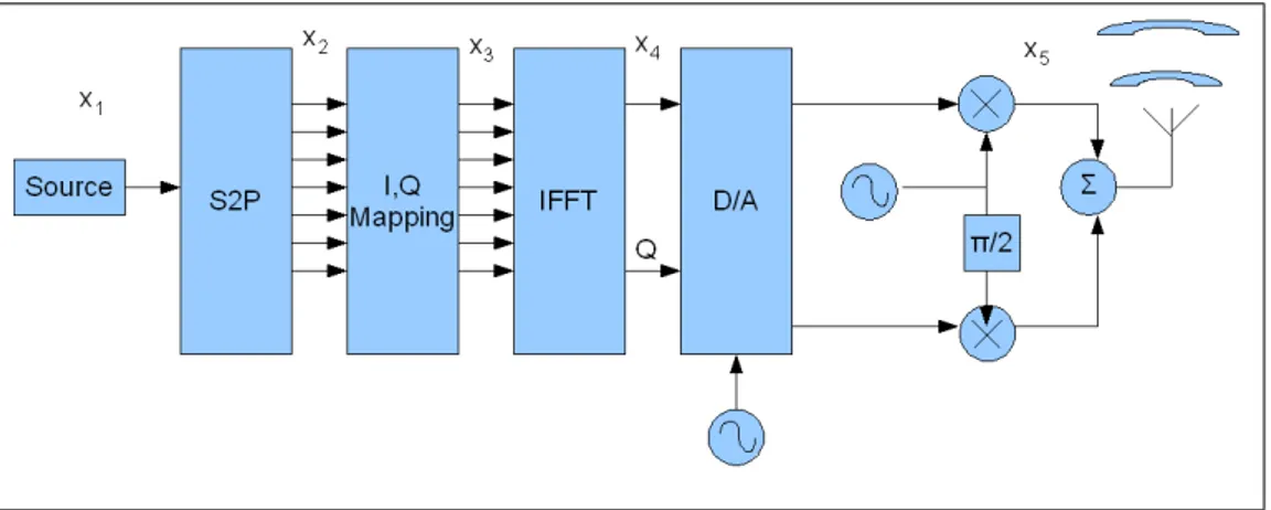
For quantifying the ICI caused by receiver ADC sampling jitter, Zero-IF trans-mitter and receiver structures which perform frequency conversions with a single
I, Q mixer are considered. The block diagrams of the OFDM transmitter and receiver that are used in the simulations are depicted in fig. 1.1 and fig. 1.2.
Figure 1.1: Zero-IF OFDM Transmitter Used in Simulations
Figure 1.2: Zero-IF OFDM Receiver Used in Simulations
˜ x[m] = 1 N N 2−1 X k=−N 2 N 2−1 X n=−N 2 ³ x[n]ej2π(k+ζ)(n−m)N ´ (1.1)
In eqn. 1.1 x[n] denotes the transmitted data, ˜x[m] denotes received data, k
denotes the time normalized to the sampling period, n denotes the frequency normalized to the system bandwidth, ζ denotes the cumulative time jitter in sampling and N denotes the total number of carriers in the system.
Jitter processes generated by the aforementioned simulation tool are injected into the communication system through the ADC depicted in fig. 2.2. In gener-ating jitter processes oscillators from different oscillator manufacturers are con-sidered. The spectral qualities of the generated processes are matched to the information on the datasheets of the oscillators that are considered. For analysis, two communication systems using OFDM as a Digital Multi-Carrier modulation method is considered. Simulations are performed on sample IEEE 802.11a and 802.15.3a communication systems and the ratio of interference power to carrier power (I/C) in OFDM carriers are computed. These kinds of ratios are important in design of communication systems since, the maximum level of noise allowed in the system is distributed among sources of noise and interference. Thus, by quantifying the interference caused by sampling jitter in the receiver ADC the other parameters in the system can be chosen such that the maximum noise and interference level in the system is kept under the limits for desired communication quality.
Based on the results obtained from the simulations, discussions are presented on the effects of the sampling jitter in OFDM communication systems. These discussions provide information on the relations between certain OFDM system
parameters and the interference created due to sampling jitter with certain spec-tral distribution. Finally, some guidelines for the design of OFDM ADC circuitry are proposed.
In Chapter 6, the conclusions obtained from the studies and the simulations carried out were stated and the thesis is concluded by pointing out to future work that may be done to further investigate the effects of timing impurities on OFDM systems.
Chapter 2
OFDM As a Bandwidth Efficient
Communication System
2.1
OFDM
In this chapter of this thesis, Orthogonal Frequency Division Multiplexed (OFDM) communication systems are examined as bandwidth efficient commu-nication systems that are effected by receiver ADC sampling jitter. OFDM parameters and the parameters that are important for the analysis of ICI effects caused by receiver ADC sampling clock timing jitter are stated.
OFDM is a digital multi-carrier modulation method. It is a communica-tion scheme that is being used increasingly in wireless communicacommunica-tion systems. OFDM has been adopted as a standard multi-carrier modulation method in com-munication systems like IEEE 802.11a, 802.11g, HIPERLAN/2, ETSI DVB-T, WiMAX and many more. The reasons behind the widespread acceptance of OFDM are listed below;
• Bandwidth Efficiency: OFDM allows high datarate transmission in a
band-width efficient manner.
• Robustness Against Multipath effects: OFDM are robust to multipath
ef-fects due to the fact that the low symbol rate in OFDM carriers
• Ease of Implementation: Modulation on orthogonal carriers can be easily
implemented using FFT and IFFT operation
The fundamentals of OFDM operation, OFDM parameters, the advantages and disadvantages of OFDM are explained in the following parts of this chapter.
2.2
OFDM Fundamentals
The first study on OFDM dates back to 1966. Robert W. Chang of Bell Labs filed a U.S patent [6] that introduced the idea of dividing the transmission bandwidth into consecutive channels and modulating parallel datastreams on orthogonal carriers without guard-band, thus performing high data-rate trans-mission in a bandwidth efficient manner. The main idea of operation in OFDM communication systems is as follows;
The source (serial data) stream is divided into parallel lower data-rate sub-streams (channels) with equal datarates, then digital modulation (mapping the symbols to the I, Q plane) is performed on the parallel data substreams. After-wards these modulated substreams are modulated with orthogonal carriers. On the receiver side, the received signal is demodulated using the same orthogonal carriers and digital demodulation is performed. Afterwards parallel datastreams (bit sequences) are demultiplexed (de-parallelized) into a single stream. These
Figure 2.1: Simple OFDM Transmitter Block Diagram
Figure 2.2: Simple OFDM Receiver Block Diagram
It is just to explain how OFDM communication systems work and state the conditions for zero Inter Symbol Interference(ISI) and zero Inter-Carrier Interfer-ence(ICI). In this respect the following part from the aforementioned patent [6] that explains zero ICI and zero ISI conditions for OFDM communication systems is presented.
Let cn represent the digitally modulated symbols that will be transmitted
through the ith channel with 1/T symbol rate, a
of the transmit filter of the ith channel and H(f ).ejφ(f ) denote the spectral
re-sponse of the transmission media. The output of the ith filter produces the
following output sequence;
c0ai(t), c1ai(t − T ), c2ai(t − 2T )... (2.1)
Thus the received sequence is as given below;
c0ui(t), c1ui(t − T ), c2ui(t − 2T )... (2.2)
Where ui(t) is the combined impulse response of the channel and the transmit
filter of the ith channel.
ui(t) =
Z ∞
−∞
h(t − τ )ai(τ )dτ (2.3)
The received signal has no Inter Symbol interference (ISI) if the Nyquist zero ISI criterion is satisfied. Namely;
Z ∞
−∞
ui(t)ui(t − kT )dt = 0, ∀k = ±1, ±2, ... (2.4)
In order to show that OFDM channels do not interfere with each other a similar path is used and conditions for zero ICI is derived.
d0uj(t), d1uj(t − T ), d2uj(t − 2T )... (2.5)
Where dn’s denote the symbols transmitted through channel j with symbol
rate 1/T and uj’s denote the combined impulse response of the jth bandpass
filter and the channel. Thus;
uj(t) =
Z ∞
−∞
h(t − τ )aj(τ )dτ = 0 (2.6)
Although the symbols received from the ithand the jthchannel overlap in time
there will be no ICI if;
Z ∞
−∞
ui(t)uj(t − kT )dτ = 0, ∀k = 0, ±1, ±2, .... (2.7)
Conditions given in eqn. 2.4 and eqn. 2.7 lead to information on the transmit filter characteristics. The Fourier transform of zero ISI criterion 2.4 states that the joint response of the transmit filter (with spectral representation Ai(f )) and
the channel (H(f )) must satisfy the following spectral properties for zero ISI.
Z ∞
0
H2(f )A2i(f ) cos(2πf kT )df = 0∀, k = ±1, ±2.... (2.8)
The Fourier transform of the zero ICI conditions give the following information about the transmit filters of the channels.
Z ∞
Z ∞
0
H2(f )A
i(f )Aj(f ) sin(βi(f ) − βj(f )) cos(2πf kT )df = 0, k = ±1, ±2....
(2.10)
Where βi(f ) and βj(f ) denote the phase response of the ith and jth channels
transmit filters. Filters satisfying these conditions are fit for OFDM communi-cations.
In [8] a method is given find and design filters satisfying the aforementioned zero ISI and zero ICI conditions. This method is left out of this work. A Sample OFDM filter bank satisfying the aforementioned conditions is given in fig. 2.3.
5 10 15 20 25 30 0 0.1 0.2 0.3 0.4 0.5 0.6 0.7 0.8 0.9 1 Frequency Amplitude−Linear Scale
Sample OFDM filters
Figure 2.3: Sample Transmit and Receive Filters For an OFDM Communication System
In this filter family the ith channel transmit filter is defined with the following
OFDM communication systems with carriers separated by frequency fs(where
fs = 1/Ts is the symbol rate of a single channel) are capable of performing data
transmission at a symbol rate of 2fs per OFDM carrier. This is a very
band-width efficient communication system, since every carrier can carry the maximum symbol rate and spectral overlap can take place as depicted in fig. 2.3. This is possible due to the orthogonality of OFDM carriers. This is, one of the many advantages of OFDM communication systems. Another advantage of OFDM is its robustness against frequency selective channel effects. Since the total band-width is divided (distributed) among carriers, the frequency selective fading will only effect certain carriers. These effects could be dealt with, by using relatively simple equalizers at the receiver. This property is very desirable to have, espe-cially in systems with high bandwidth because it reduces the complexity of the OFDM receiver.
Another reason for OFDM to be a widely used multi-carrier modulation method is due to the ease of implementation. The modulation of substreams onto orthogonal carriers and the filtration which enables the spectral efficiency of OFDM can be implemented by an IFFT (Inverse Fast Fourier Transform) operation at the transmitter and a FFT (Fast Fourier Transform) operation at the receiver. The advances in microprocessor technologies enables high data-rate OFDM systems to be implemented with a single microprocessor. OFDM carriers generated from an IFFT operation is depicted in the frequency domain in fig. 2.4 and in time domain in fig. 2.5.
OFDM has its disadvantages as well. The orthogonality property of OFDM that enables OFDM to be a bandwidth efficient communication system causes OFDM systems to be very vulnerable to synchronization errors. Due to the fact that neighbouring channel rejection (filtering) depends only on orthogonality, any synchronization error effecting the orthogonality of OFDM carriers causes
leakage through (and between) the OFDM channels. These leakages result in quick decreases in the the Signal to Noise Ratio (SNR) in OFDM channels, leading to an increase in Bit Error Rate (BER).
Another disadvantage of OFDM communication systems is that they require very linear amplifiers. The crest factor (Peak Power to Average Power ratio) in OFDM systems can get very high. This is possible, since symbols on different carriers can align in phase and cause very large signal levels that can push the power amplifiers at OFDM transmitters to saturation. The crest factor depends on the number of carriers and the type of constellation mapping used in the system. In OFDM systems crest factors can go as high as 12 dB [30]. This systems require highly linear power amplifiers and high back-off values in OFDM transmitters. 1 2 3 4 5 6 7 8 −0.4 −0.2 0 0.2 0.4 0.6 0.8 1 subcarrier number amplitude
Figure 2.4: OFDM Filters Created by IFFT Operation For an Eight Channel OFDM System(Frequency Domain)
0 0.2 0.4 0.6 0.8 1 1 2 3 4 5 6 7 8 −1 0 1 subcarrier number time amplitude
Figure 2.5: OFDM Filters Created by IFFT Operation For an Eight Channel OFDM System(Time Domain)
In order to carry out the analysis, OFDM communication equations must be derived using the communication system that is assumed. In this thesis, a typical OFDM communication system with zero-IF architecture using a IFFT for the multi-carrier modulation and FFT as the multi-carrier demodulation method is considered. Figure 2.6 depicts such a transmitter using IFFT for multi-carrier modulation and fig. 2.7 depicts the matching receiver.
Figure 2.6: Block Diagram of an OFDM Transmitter Using IFFT For Multi-Carrier Modulation
Figure 2.7: Block Diagram of an OFDM Receiver Using FFT For Multi-Carrier Demodulation
The signals and the operations on the signals through the marked nodes on the block diagrams are explained below;
The input datastream consisting of a bit sequence will be parallelized accord-ing to the number of parallel channels in the system. In an N-channel OFDM communication system, if the input consisting ofof N symbols is denoted by ~x1
the signal at x2 is x2 = ~x1t, meaning the input symbol stream is parallelized. In
short, the 1 by M stream is multiplexed into N by M/N substreams throughout serial to parallel converter.
After the datastream is parallelized, the digital modulation(constellation map-ping) is performed. The order of multiplexing and constellation mapping oper-ations can be interchanged. At node x3 N substreams consisting of complex
symbols on the I, Q plane are present.
Multiplication with the complex exponents in the IFFT operation results in modulation onto orthogonal carriers. The mathematical formulation is shown below;
X[k] = N 2−1 X n=−N 2 x[n]ej2πkn/N (2.12)
In eqn. 2.12, k denotes the time index normalized to the symbol period Ts,
n denotes the frequency index normalized to the symbol rate fs and N denotes
the total number of carriers in the communication system. Notice that IFFT operation with the complex multiplication operations corresponds modulating the low datarate substreams onto orthogonal frequencies with frequency index
n. The real and imaginary components of the IFFT output are separated into I
and Q components for frequency upconversion.
After the substreams are modulated onto orthogonal carriers, they are input to Digital to Analog Converter(DAC) and frequency upconversion is performed at x5 with an I, Q mixer and a local oscillator. The output of the transmitter is
given in eqn. 2.13. s(t) = √1 N N 2−1 X n=−N 2 (x[n]ej2πkn/N)ejωtrt (2.13)
The signal detected at the receiver antenna x6 undergoes I, Q frequency
down-conversion using two oscillator signals locked in 90 deg phase and an I, Q mixer. The resulting I and Q signals are digitized using a ADC. At x7 the frequency
downconversion is completed and the orthogonally modulated carriers are at baseband.
The digitized I and Q signals are input to a processor and FFT is performed on these signals. Afterwards the complex symbols on the I, Q plane are de-mapped onto parallel bit sequences. After x9, bit sequences are demultiplexed(serialized)
and after the parallel to serial conversion the data transmission is complete. The formula at the output of the receiver is given eqn. 2.14 the simplified version of the equation is given in eqn. 2.15.
˜ x[m] = 1 N N 2−1 X k=−N 2 N 2−1 X n=−N 2 (x[n]ej2πkn/N)e−j2πkm/Nejωtxte−jωrxt (2.14) ˜ x[m] = 1 N N 2−1 X k=−N 2 N 2−1 X n=−N 2 (x[n]ej2πk(n−m)/N)ej(ωtx−ωrx)t (2.15)
In 2.15, k denotes the time index normalized to Ts, n denotes the frequency
index on the transmitter side normalized to the symbol period fs, m denotes
the frequency index on the receiver side normalized to the carrier spacing, N denotes the total number of carriers in the system, ωtx and ωrx denote the radial
frequencies of the frequency conversion oscillators at the transmitter and receiver respectively.
In order to understand how the communication system works one can examine eqn. 2.15. It can be seen that the output ˜x[m], is equal to the input x[n] when n = m and ωtx= ωrx. Note that if n 6= m and ωtx = ωrx, ˜x[m] = 0. This means,
there is no Inter-Carrier Interference from carrier n to carrier m. This condition is actually a discrete equivalent of the zero ICI condition given in eqn. 2.7.
Note that receiving the transmitted signal correctly highly depends on the or-thogonality of carriers. If ωtx6= ωrx or there is some frequency errors during the
FFT or IFFT operations the carriers will quickly leak into each other causing In-terference in neighbouring carriers. These kinds of errors are named as frequency offsets. These errors can be dealt with using carrier recovery methods, [15],[20] gives details on several carrier recovery algorithms.
The basic idea behind carrier recovery relies on estimating the frequency offset between transmit receive signals and compensating for these offsets. This com-pensation is done by de-rotating the I, Q (constellation) plane with the offset frequency between the transmitter and the receiver.
Estimation of the frequency offsets are generally done with OFDM pilot signals. Pilot signals are signals with known content that are transmitted through certain OFDM carriers. At OFDM receivers, the degradation on the pilot signals are used as observations to estimate the effects of the transmission medium on the OFDM carrier. Pilot signals can be also used to compensate for the ICI effects caused by the phase noise of the local oscillators performing frequency conversion. This effect and some mitigation techniques are presented in Chapter 4.
Even if there are no frequency offsets between carrier frequencies of the trans-mitter and the receiver (meaning they synchronized in terms of frequency), there may be rapid fluctuations in the phase that cause the carrier spectrum to broaden and degrade the orthogonality of OFDM carriers. Also, even if there are varying timing errors between the transmitter and receiver, the orthogonality of carriers will not be met. The varying phase difference in the oscillator is caused phase noise of the oscillator and the varying timing drifts is caused by timing jitter in sampling instants. The effect of these impurities on OFDM will be presented in Chapter 4. These rapid fluctuations in the phase and timing do not degrade
the SNR in OFDM carriers as much as frequency offsets but these effects are bottlenecks[27] for efficient communication and they need to be quantified for efficient designs.
2.3
OFDM Parameters
In this section, the OFDM system parameters are stated. The fundamental parameters of an OFDM system are listed below;
• System Bandwidth: Total bandwidth in which data transmission occurs.
The unit for bandwidth is Hertz (Hz).
• Symbol Rate: Total symbol rate carried over the bandwidth. The unit for
Symbol rate is symbols per second.
• Data Rate: The data rate carried over the communication system. This
value depends on the type of constellation mapping used in the system. For a data communication system using 4-QAM data rate is double the symbol rate. The unit for data rate is bits per second.
• FFT Size: The total number of carriers in the system.
• Effective Number Of Carriers: The number of carriers excluding the
num-ber of unused carriers and pilot carriers in the system.
• Cyclic Prefix or Guard Time: In the beginning of an OFDM symbol, a
certain portion from the end of the same symbol is placed. This is to prevent Inter Symbol Interference due to multipath effects and the value of this parameter depends on the delay spread of the environment. The unit for guard time is seconds.
From the parameters given above the parameters that are important for the analysis in this thesis are the total number of carriers, bandwidth and digital modulation type.
In this chapter OFDM based communication systems were examined. OFDM properties and fundamentals of OFDM communication systems were presented. The informative background presented here will be used for analyzing the effects of receiver ADC timing jitter on OFDM communication systems.
Chapter 3
Oscillator Fundamentals and
Timing Impurities of Oscillators
3.1
Oscillator Fundamentals
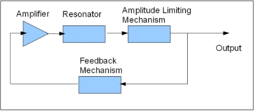
An oscillator is an electronic circuit that outputs a periodic waveform with de-termined frequency. The output has a certain amplitude, frequency and phase. Oscillators are used as timing elements in electronics systems. They are key elements in frequency conversion applications along with mixers. They also pro-vide timing information to various digital components. A typical oscillator block diagram is given in fig. 3.1
An oscillator consists of a frequency selective element (resonator), an active device (amplifier), an amplitude limiting mechanism and a positive feedback from the output to the input. The oscillator depicted in fig. 3.1 works as explained below;
Figure 3.1: Typical Oscillator Block Scheme
The thermal noise inherent in the system is amplified by the amplifier. The resonator filters out the undesired frequency components in the signal and the positive feedback mechanism creates instability in the system causing the system to output a signal with increasing amplitude. Certain amplitude limiting mech-anisms are placed in the oscillators to control the amplitude of the oscillation. Thus the oscillator outputs a signal with certain amplitude at steady-state. The frequency content of the output signal is determined by the characteristics of the resonator.
If the feedback mechanism is not set properly, the depicted oscillator is essen-tially a (frequency) tuned amplifier. There exists a condition to guarantee the oscillation. This condition is known as the Barkhausen oscillation condition[12]. This condition essentially states, the need for an unstable loop to create a grow-ing signal which reaches to a stable amplitude after the transient effects wear out.
The oscillator parameters that can be found on a datasheet are listed below;
• Frequency of oscillation: Defines the center frequency of the resonator used
in the oscillator. The unit for this parameters is Hz.
• Tuning: If the resonator of the oscillator can be tuned in a certain frequency
range the oscillator is said to be tunable. Tunable oscillators are very widely used in communication systems. The unit for this parameter is Hz.
• Frequency stability: Oscillation frequency of an oscillator tends to drift
with time. There are many reasons for the oscillation frequency to drifts. Some examples causing frequency drift are; temperature changes in the system, the effect of ageing in various components of the oscillator, mi-crophonic (vibration based) effects etc. The units for frequency stability is given ppm(parts per million). For example, the frequency stability of a crystal oscillator could be given as ±1 ppm in the temperature range
−40 + 85◦C. This would mean an oscillators central oscillation frequency
will deviate from its central oscillation frequency by a fraction of 10−6 (i.e
if the oscillator has central oscillation frequency of 10 MHz, 1 ppm drift would result in 10Hz frequency drift causing the oscillator to oscillate at a frequency of 10MHz ± 10 Hz.
• Frequency push: The variations in the supply voltages cause the resonator
center frequency to change resulting in a drift in the oscillation frequency, the amount of frequency drift caused by supply voltage variation is called frequency push. The unit for frequency push is Hz/Volts.
• Frequency pull: The variations on the load of the oscillator loads the
res-onator and causes frequency drifts in the center frequency of oscillation. The frequency drift, caused by loading, is named as frequency pull. The unit for frequency pull is Volts/Ω.
• Phase noise: Phase noise is a parameter defining the spectral purity of the
oscillator, it is closely related to the wandering in the phase of oscillation. The unit for phase noise is dBc/Hz.
In this thesis, the focus is mainly on short term non-static impurities on the phase of oscillators. This does not mean that other impurities are not important in OFDM systems. On the contrary, the orthogonality is drastically effected by all sorts of synchronization errors, such as frequency offsets and drifts in central oscillation frequency. These topics are well studied and these problems can be handled with carrier recovery algorithms. Some studies on carrier recovery algorithms are given in [15],[20]. Also, frequency offsets in oscillators due to ageing and temperature changes are processes that are relatively slow processes. These impurities can be considered as frequency offsets. The frequency drifts due to power supply and load instabilities can be decreased by providing isolation to the resonator from the source and the load as much possible. However, phase noise is not so easily handled. The rest of this chapter focuses on, phase noise and jitter as oscillator impurities and presents models for these impurities.
3.2
Phase Noise and Phase Noise Definition
The phase noise of an oscillator is a spectral quantity describing the purity of an oscillator and the short time fluctuations in the phase of oscillation. These kinds of timing impurities (along with frequency offsets) cause Inter-Carrier In-terference(ICI). These effects cannot be dealt with, by using carrier recovery methods.
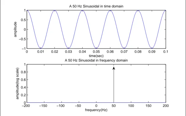
The output of an ideal oscillator is expected to be a pure sinusoidal. The output of the ideal oscillator is in the following form;
Where, Av denotes the amplitude of oscillation, fosc denotes the frequency of
oscillation and φ denotes the phase of the oscillation. This oscillator output corresponds to a pure dirac-delta function in the frequency domain. Figure 3.2 demonstrates the output of an ideal oscillator in time and frequency domain.
0 0.01 0.02 0.03 0.04 0.05 0.06 0.07 0.08 0.09 0.1 −1 −0.5 0 0.5 1
A 50 Hz Sinusoidal in time domain
time(sec) amplitude −2000 −150 −100 −50 0 50 100 150 200 0.2 0.4 0.6 0.8 1
A 50 Hz Sinusoidal in frequency domain
frequency(Hz)
amplitude(log scale)
Figure 3.2: Output of an Ideal Oscillator
However, real oscillators have all kinds of impurities. The amplitude of oscilla-tion, Av may have some randomness. There may be drifts in fosc, the frequency
of oscillation and random phase fluctuations in φ(t) may be observed at the out-put of the oscillator. All of the mentioned impurities, may be caused by intrinsic effects or caused by external perturbations. In any case they, will degrade the purity of the oscillator and limit the performance of the communication system. Figure. 3.3 depicts an example for the output of an oscillator with impurities.
0 0.02 0.04 0.06 0.08 0.1 −1 −0.5 0 0.5 1
A 50 Hz Sinusoidal with impurities in time domain
time(sec) amplitude(volts) −500 0 500 −20 −10 0 10 20
Power Spectral Density of a real 50 Hz sinusoidal
frequency(Hz)
amplitude(dBW/Hz)
Figure 3.3: Output of a Real Oscillator
In early studies, phase noise was defined as follows;
For an oscillator with central oscillation frequency, fosc, phase noise at
fre-quency fosc+ ∆f is the ratio of the power measured at fosc+ ∆f (in one hertz
bandwidth), to the total power of the carrier.
This definition is ambiguous, because it includes the spectral broadening due to other effects, such as amplitude noise. Later, a phase noise definition was given by IEEE standard 1139-1999. This definition isolated phase and amplitude noise in oscillators. This standard defines phase noise using the power spectral density of the phase function in the oscillation Sφ(f ). According to this standard the
phase noise at frequency fosc+ ∆f is defined as; half of the power level in one Hz
bandwidth measured at offset frequency fosc+ ∆f [22]. Phase noise has units of
The mathematical expression for the definition of phase noise is given in eqn. 3.2;
L(fosc+ ∆f ) =
1
2Sφ(fosc+ ∆(f )) (3.2)
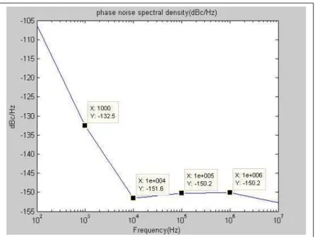
Figure 3.4: Sample Phase Noise Plot of an Vectron VCC6-QCD-250M000 Oscil-lator [31]
3.3
Phase Noise Models
In order to examine a system one has to develop and assume some models for the elements in the system (i.e assuming small signal models for analyzing am-plifier blocks or assuming a noise source and noiseless elements to perform noise analysis). In order to understand the effects of phase noise on communication
Phase noise is often modelled as a Wiener random process (Brownian motion). This means that the phase of an oscillator performs a random walk with time. It will be just to mention, the main properties of a Wiener random process. The main properties of Wiener random processes are listed below;
• W0 = 0, starting point of the process is zero by definition.
• The wandering of the process is continuous.
• E[Wt] = 0 The mean of the Wiener process is zero.
• E[WtWs] = min(t, s) this is the auto-correlation function of the Wiener
random process. This implies that the phase wanders boundlessly as time passes.
• Increments of Wt on non overlapping intervals are independent.
This process is not a wide sense stationary process, meaning that the statis-tical properties (autocorrelation function) of the process cannot be expressed as a function of the time difference between delayed Wiener processes. It is not mathematically correct to mention a Power Spectral Density(PSD). This is one of the challenging parts of working with phase noise.
The wandering of the phase of an oscillator output is modelled by a random walk. The amount or strength of the phase noise on a particular oscillator output will be defined by certain parameters of the oscillator. Various models have been developed to model oscillator phase noise. In the following section, several oscillator phase noise models will be explained.
3.3.1
Oscillator Phase Noise Models
One of the earliest studies on oscillator phase noise modeling was published in 1966 by D. B. Leeson[2]. This study presents a model to determine the phase noise spectrum for oscillators. The model accounts for and builds up on the spectral characteristics of the resonator, the effective noise figure of the oscillator, the 1/f noise characteristics of the active device used in the oscillator and the signal level at the input of the oscillator active device. The phase noise model offered by this study is as below;
Sφ(wm) = · α ωm+ 2F kT /Ps ¸· 1 + ( ω0 2Qωm )2 ¸ (3.3) In this equation;
• α represents a constant determined by the 1/f noise corner of the active
device,
• F is the noise figure of the active device used in the oscillator, • k is the Boltzmann constant,
• Ps is the signal level entering the active device of the oscillator,
• ω0is the central oscillation frequency,
• Q is the quality factor of the resonator used in the oscillator, • ωm is the offset frequency at which phase noise is calculated,
stat-Another oscillator phase noise model is proposed in [3]. In this study, the authors assume a linear periodic-time variant model for the oscillator. This as-sumption depends on, the periodic nature of the oscillator and the time variant response of the oscillator to injected noise currents. An oscillator injected with noise at the peak of the oscillation does not create any phase error, but cre-ates randomness in the amplitude. However, if noise is injected during the zero crossing of the oscillator causes the maximum phase error.
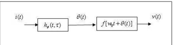
With the linear periodic time variant oscillator assumption, the study bisects the injected noise to phase noise conversion in two steps; first, they define the injected noise to phase transfer function.
hφ(t, τ ) = Γ(ω0τ )
qmax
u(t − τ ) (3.4)
Where Γ(x) denotes the Impulse Sensitivity Function (ISF), qmax is the
maxi-mum charge displacement across the capacitor and u(t) is the unit step function. This impulse response function represents the change of phase, in an oscillator, when an impulse current is injected at phase ωoτ . Here it is just to explain the
ISF denoted as Γ(x). This function is a dimensionless, frequency and amplitude independent 2π periodic function which is named as the Impulse Sensitivity Func-tion. The ISF gives information on the sensitivity of the oscillator to injected noise current at various phases. The calculation of this function is explained in detail in [3]. The output of the injected noise to phase transfer function will un-dergo a phase to voltage transformation and produce phase noise. The injected noise to phase noise conversion mechanism is simply the phase modulation of the output waveform. Figure 3.5 depicts the two step injected noise to phase noise conversion mechanism.
Figure 3.5: Injected Noise to Phase Noise Conversion Mechanism
By the help of the parameters above, the phase noise spectrum of an oscillator is characterized. For the 1/f2 region the phase noise spectrum is given by;
L(∆ω) = 10log µ i¯2 n ∆fΓ2rms 4q2 max∆ω2 ¶ (3.5)
Where in denotes the noise current ,Γrms is the rms value of the ISF.
For the 1/f3 region, the phase noise spectrum of the oscillator is given by
L(∆ω) = 10log µ ω 1/fc20 ¯ i2 n ∆f 8q2 max∆ω3 ¶ (3.6)
Where indenotes the noise current c0 denotes the first Fourier series expansion
coefficient of the periodic ISF and ω1/f is the 1/f corner frequency.
For further frequency offsets from the oscillation, the phase noise converges to the phase noise model proposed by Leeson.
This oscillator phase noise model adds improvements to the Leeson phase noise model through the calculation of the ISF and incorporating the 1/f2 and 1/f3
The final oscillator phase noise model investigated in this thesis is the model by Demir et al.[5]. In this study, oscillator phase noise is examined rigorously without any assumptions(such as, high Q assumption for the resonator). This study performs a non-linear perturbation analysis and shows that orbital (am-plitude) deviations remain small, for small perturbations, but the perturbations in the phase can grow unboundedly large with time. These findings fit the be-haviour of phase noise in oscillators as the phase uncertainty in oscillators grows unboundedly with time. The variance of the phase uncertainty is modelled as linearly increasing.
After this analysis, the study characterizes the Probability Distribution Func-tion (PDF) of phase noise and derives the power spectral density of an oscillator with phase noise.
S(ω) = ∞ X i=−∞ XiXi∗ ω2 0i2c 1 4ω40i4c2+ (ω + iω0)2 (3.7)
Where Xi’s denote the Fourier coefficients of the periodic unperturbed
oscil-lation and c denotes the linear increase in the variance of the phase uncertainty in the phase of the oscillation.
The mentioned oscillator phase noise models are very useful for designing os-cillators with low phase noise specifications, because they provide insight on the phase noise phenomenon and its sources in oscillators.
3.4
Jitter and Phase Noise to Jitter Conversion
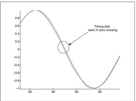
In order to investigate the effect of Analog Digital Converter (ADC) sampling jitter, it will be useful to investigate jitter and phase noise to jitter conversion. The next section explains the jitter and jitter to phase noise conversion. Jitter is defined as the variations in the periodic behaviour of a signal. Jitter is measured by the RMS values of the deviation of the periodic signal from the ideal periodic signal. The units for jitter is given in seconds for time jitter and in radians for phase jitter. Figure 3.6 depicts the timing jitter in a sinusoidal signal.
80 85 90 95 −1 −0.8 −0.6 −0.4 −0.2 0 0.2 0.4 0.6 0.8 Timing jitter seen in zero crossing
Figure 3.6: Illustration of Timing Jitter
The output of an oscillator and the component causing jitter should be exam-ined, in order to derive a conversion from phase noise to timing jitter.
In eqn. 3.8, Av denotes the amplitude of the oscillation and the argument of
sinusiodal is the phase. Thus, the statistcs of φ(t) represent the phase jitter (deviation from the expected output phase) in radians. In order to find the timing jitter, the phase deviation should be divided by the radial frequency of oscillation namely, timing jitter tj = 2πfφosc. In order to find the rms power of
jitter, the power spectral density of φ(t) should be integrated in the bandwidth of interest[26]. The expression for calculating rms power of phase jitter is given in eqn. 3.9 and for timing jitter rms power calculation is given in eqn. 3.10.
Ppj = sZ BW Sφ(f ) (3.9) Ptj = 1 2πfosc sZ BW Sφ(f ) (3.10)
In this chapter, the fundamentals of oscillators and timing impurities on oscilla-tors were presented. Furthermore, oscillator parameters and oscillator impurities that are important for quantifying the ICI effects on OFDM communication sys-tems caused by timing jitter on receiver ADC were stated. A summary of the previous studies on phase noise, phase noise models and oscillator phase noise models was presented. The information presented here will provide the basis for the analysis and the simulations presented in Chapter 5.
Chapter 4
Inter-Carrier Inteference Effects
on OFDM Systems
In the previous chapters, a large portion of the literature review was presented. This review involved information on oscillators and OFDM communication sys-tems that is necessary to analyze the effects of timing jitter in receiver ADC sampling clocks on OFDM based communication systems.
In this chapter, a summary of existing work on the ICI caused by phase noise in OFDM local oscillators and the ICI caused by ADC sampling jitter is presented.
4.1
The ICI Effects of Local Oscillator Phase
Noise on OFDM Communication Systems
In this section, the previous studies on ICI caused by the phase noise of the local oscillator driving the mixers that perform the frequency upconversion and
The local oscillators causing ICI in OFDM communication systems are shown in fig. 4.1 and fig. 4.2. Notice that, the transmitter and the receiver are in zero IF configuration.
Figure 4.1: OFDM Transmitter Block Diagram Displaying the Transmit Local Oscillator Causing ICI
Figure 4.2: OFDM Receiver Block Diagram Displaying the Receive Local Oscil-lator Causing ICI
The equation for OFDM communication was given in eqn. 2.15. If there is no frequency offset between the carrier and the receiver the received signal is similar to eqn. 2.15. However, the difference between the transmitter and receiver phase noise is multiplied with the signal as shown below;
˜ x[m] = ½ 1 N N 2−1 X k=−N 2 N 2−1 X n=−N 2 (x[n]ej2πk(n−m)N ) ¾ ej(φtr(t)−φrx(t)) (4.1)
In eqn. 4.1, φrx(t) denotes the phase noise of the local oscillator at the receiver.
Notice that if n = m and φtx(t) − φrx(t) = 0, the OFDM system works properly.
However, the phase fluctuations in the transmitter and receiver local oscillator namely, φtx(t) and φrx(t), prevent the system from having perfect
synchroniza-tion. Thus, the orthogonality is degraded by the phase noise in the receiver and the transmitter. The error signal can be found by subtracting the ideal output from the output obtained in eqn. 4.1. Then, interference power in a certain OFDM channel can be calculated using the error signal shown in eqn. 4.3.
err(t) = ½ 1 N N 2−1 X k=−N2 N 2−1 X n=−N2 (x[n]ej2πk(n−m)N ) ¾ − ½ 1 N N 2−1 X k=−N2 N 2−1 X n=−N2 (x[n]ej2πk(n−m)N ) ¾ ej(φtr(t)−φrx(t)) (4.2) err(t) = ½ 1 N N 2−1 X k=−N 2 N 2−1 X n=−N 2 (x[n]ej2πk(n−m)N ) ¾ (1 − ej(φtr(t)−φrx(t))) (4.3)
This error consists of two parts; the first part is due to the common phase rotation in the I, Q plane. This part is caused by the mean of the error signal. This portion of the error is called Common Phase Error (CPE). The second
This ICI effects can be prevented by using ICI removal algorithms at the receiver. In the next section, previous studies that have worked on the removal of these effects are reviewed.
4.1.1
Mitigation From ICI Due to Local Oscillator Phase
Noise
Numerous studies have been performed to analyze the local oscillator ICI ef-fects. Some solutions for the removal of these effects have been proposed in [23],[24].
The ICI removal algorithms depend on estimation of the phase noise waveform causing ICI and removing these effects by de-rotating the I,Q plane to compen-sate for the phase noise effects. The OFDM pilot signals provide a base for estimations. Since the pilot signals are signals with known content, the effects due to channel and phase effects can be estimated and compensated.
In [23], the phase noise waveform is estimated by using a Kalman filter. In this study perfect frequency and timing synchronization is assumed. In this model, the received signal is shown as in eqn. 4.4.
r(n) = (x(n) ⊗ h(n))ejφ(n) + ζ(n) (4.4)
In eqn. 4.4 x(n) denotes the data that is transmitted by the transmitter, h(n) denotes the impulse response of the transmission medium, ζ(n) denotes the Ad-ditive White Gaussian Noise(AWGN) in the communication system, ⊗ denotes circular convolution operation and φ(n) denotes the phase noise effecting the
After performing FFT at the receiver, the mth symbol at the lth channel is found as; Rm,l= Xm,lHm,lIm(0) + N −1 X n=0,n6=l Xm,nHm,lIm(l − n) + ηm,l (4.5)
In this equation, Im represents the discrete spectral realization of the phase
noise exponential ejφ(t), during the mth symbol duration.
After this characterization, the authors place a model for the phase noise func-tion. They model phase noise by a random walk. The phase noise is generated using eqn. 4.6.
φ(n) = φ(n − 1) + ω(n) (4.6)
Where ω(n) is a Gaussian random process with zero mean and variance 4π2f2 ccTs.
Using these two models for phase noise and the OFDM system the phase noise is estimated using a Kalman filter and de-rotation is performed. Details of this algorithm can be found in [23].
In [24] the ICI effects are removed using the spectral estimates of phase noise. The communication system is modeled as done in [23]. The communication equation is as shown in eqn. 4.4. One example for the spectral estimation of phase noise is presented in fig. 4.3. The details of the estimation method can be found in [24].
0 50 100 150 200 250 300 350 400 450 500 −0.08 −0.06 −0.04 −0.02 0 0.02 0.04 0.06 0.08 0.1 time index
Estimating the phase noise waveform spectrally
Zero order estimate
Phase noise waveform
First order estimate
Second order estimate
Figure 4.3: Example for Spectral Phase Noise Estimation
After the estimation of the phase noise waveform is complete, the ICI can be compensated by de-rotating the I, Q plane according to the estimates. The better the phase noise is estimated, the lower the residual ICI.
4.2
The ICI Effect Due to The Timing Jitter on
Receiver ADC
In this section, a summary of the previous work on ICI caused by the timing jitter on OFDM receiver ADC’s is presented. The common practice in these studies is to introduce models for OFDM systems and sampling jitter, followed by performing analysis and simulations using these models.
In [17] the OFDM system model is presented with the following equations. Equation 4.7 shows the model for the transmitted OFDM signal and eqn. 4.8 shows the signal received that is subject to sampling jitter.
s(t) = N 2 X k=−N 2+1 skej2πfkt (4.7) s(n∆t + τn) = N 2 X k=−N 2+1 skej2πfk(n∆t+τn) (4.8)
As it can be seen from eqn. 4.8, this study assumes a perfect transmission medium and no other impurities except sampling jitter in the system. In the equations given above, k denotes the frequency index, n denotes the time index, ∆t denotes the sampling period and τ denotes the timing jitter in sampling time.
In this study, timing jitter is assumed to be a Wide Sense Stationary(WSS) Gaussian process with zero-mean and variance, σ2
j. Afterwards, correlation
coeffi-cients between jitter samples have been assumed. The assumed correlation coef-ficients (Gaussian and exponential correlation respectively) are given in eqn. 4.9 and eqn. 4.10.
ρ(t) = e−β2t2 (4.9)
ρ(t) = e−αt (4.10)
Where α and β are positive numbers dictating the correlation between jitter samples.
ˆ sm = 1 N N 2 X n=−N 2+1 s(n∆(t) + τn)e −j2πmn N (4.11) ˆ sm = N 2 X k=−N 2+1 sk µ 1 N N 2 X n=−N 2+1 ej2πN (k−m)nej2πfkτn ¶ (4.12)
Afterwards, eqn. 4.12 is separated into two parts which show the Inter-Carrier Interference(ICI) and Common Phase Error(CPE). This bisection is shown in eqn. 4.13
ˆ
sm = ηmsm+ αm (4.13)
Where αm denotes the ICI introduced and ηm denotes the common phase error.
αm and ηm are given in open form below;
αm = N 2 X k=−N 2+1,l6=m sk µ 1 N N 2 X n=−N 2+1 ej2πN (k−m)nej2πfkτn ¶ (4.14) ηm = 1 N N 2 X n=−N 2+1 ej2πfkτn (4.15)
After these characterizations, ICI levels are determined by using the afore-mentioned characterizations on the jitter correlation ρ(t). The details of the calculations and results can be found in [17].
In [18] a similar method is used for the characterization of ICI. The OFDM transmit signal is given as;
s(t) =
N −1X k=0
Skej2πk∆f t (4.16)
Where, sk denotes the symbols to be transmitted and k is the carrier index.
The the signal obtained after it has been demodulated using orthogonal carri-ers(FFT operation) is as given below;
ˆ sk = 1 N N −1X l=0 sl N −1X n=0 ej2π(l−k)nN ej2πlδnT (4.17)
Where, δn denotes the jitter at the receiver sampling instant. The assumption, δn
T << 1 simplifies eqn. 4.17 into the following form.
ˆ sk= 1 N N −1X l=0 sl N −1X n=0 ej2π(l−k)nN µ 1 + j2πlδn T ¶ (4.18)
Noting that the error signal is defined as ˜sk = ˆsk−skand using this information
together with eqn. 4.18, the error signal due to sampling jitter at the OFDM receiver is shown below;
˜ sk= 1 N N −1 X l=0 slj2πl µN −1X n=0 ej2π(l−k)nN δn T ¶ (4.19)
After this characterization calculations on ICI are made and signal to inter-ference ratios are calculated. Further information on the results can be found in [18].
The main difference between the aforementioned studies and the analysis pre-sented in this thesis is the synthesis of colored jitter processes. Synthesizing receiver ADC jitter with its spectral characteristics will help quantify the ICI effect created by OFDM receiver more accurately. In [17], it is stated that Gaus-sian and exponential correlation functions have been assumed, because no model exists describing correlation function of jitter. This thesis does not offer a model for jitter correlation, instead ICI is calculated by generating a process that sim-ulates the behaviour of a certain ADC circuitry.
In this chapter, the previous work on ICI effects caused by the phase noise of the local oscillators performing the frequency conversion in OFDM systems were reviewed. Also, a review of the previous work on the ICI effects due to OFDM sampling jitter was presented. These studies provide the basis for the analysis in the next chapter.
Chapter 5
Simulations on Receiver ADC
Timing Jitter ICI Effects
In this chapter, the simulations that are performed for quantifying the ICI effects caused by timing jitter in OFDM receiver ADC’s are presented. For per-forming these simulations, a simulation tool that can generate phase noise with defined spectral qualities was prepared. The MATLAB source code of this tool can be found in Appendix A. With this tool, close-in phase noise spectral density resulting from random walk in oscillator phase and the white portion of phase noise that is observed at high frequency offsets can be generated. In order to investigate the ICI effects created by the generated phase noise processes, an-other simulation tool that computes the ratio of the interference power to carrier power ratio created by the sampling jitter on OFDM receiver ADC was prepared. Using these two tools the ICI created by sampling jitter on OFDM receiver ADC is computed for various OFDM systems that are subject to sampling jitter with defined spectral characteristics at the OFDM receiver. Discussions are presented on the resulting ICI plots and guidelines are proposed for the design of OFDM
5.1
Generating Phase Noise With Certain
Spectral Characteristics
The typical phase noise spectral density of an oscillator consists of a random walk portion and a white phase noise skirt that the phase noise spectrum settles to at higher offsets, to generate this spectrum first the white noise portion of phase noise was generated. This way the spectral density of the created white phase noise can be verified analytically and the power spectral densities of the created processes can be verified.
For a generated white phase noise sequence of an oscillator at frequency fosc,
that has standard deviation σj, the power spectral density for the timing jitter
can be calculated by spreading the jitter power over the Nyquist bandwidth using eqn. 5.1. St(f ) = σ2 j fosc (5.1)
For phase jitter the power spectral density obtained in eqn. 5.1 must be multiplied by 2πfosc.
Sφ(f ) = St(f ) × (2πfosc)2 (5.2)
Using the equations aforementioned above white phase noise was generated. The obtained power spectral density was verified. For a 250 MHz oscillator with 300 ps standard deviation, the timing jitter power spectral density can be
St(f ) = σ2 j fosc = (3 × 10 −13)2 250 × 106 = 3.6 × 10 −34 (5.3) Sφ(f ) = St(f )×(2πfosc)2 = 3.6×10−34×(2π250×106)2 = 8.9×10⁻¹⁶ ' −150.5dBc/Hz (5.4)
The measured phase noise power spectral density for the sample oscillator is as depicted in fig. 5.1.
Figure 5.1: Sample Phase Noise Plot of an Vectron VCC6-QCD-250M000 Oscil-lator [31]
The synthesized white phase noise has the power spectral density depicted in fig. 5.2.
Figure 5.2: Synthesized White Phase Noise
It can be seen that the analytically determined white phase noise power level is obtained with the synthesized phase noise and it is representative of the sample oscillator depicted in fig. 5.1. Figure 5.2 is obtained by performing Monte carlo simulations that apply the Fourier transform of the autocorrelation function (Calculate the Power Spectral Density). Details can be found in Appendix A.
After being able to synthesize white phase noise with determined spectral density random walk was superposed to create a realistic phase noise spectrum. Random walk phase noise was generated using eqn. 5.5.
φ[n] = φ[n − 1] + N(0, σ22πf
osc) (5.5)
was checked to verify the input. As stated in Chapter 3 random walk is not a Wide Sense Stationary(WSS) process. This means that, Power Spectral Density can not be computed in a straightforward manner. Still, the Fourier transform of the autocorrelation function will give a good estimate of the Power Spectral Spectral Density of the synthesized phase noise.
Sφ(f ) =
Z
Rφ(τ )ej2πf τdτ − (2πfosc) (5.6)
Equation 5.6 shows the phase noise power spectral density. In logarithmic scale the units for the output is dBc/Hz. Figure 5.3 shows the phase noise power spectral density for the synthesized phase noise
Figure 5.3: Phase Noise Power Spectral Density Created by a Random Walk with Step Strength 1fs and 400fs White Phase Noise on a 250 MHz Oscillator
![Figure 5.1: Sample Phase Noise Plot of an Vectron VCC6-QCD-250M000 Oscil- Oscil-lator [31]](https://thumb-eu.123doks.com/thumbv2/9libnet/5735495.115255/62.892.262.695.511.842/figure-sample-phase-noise-plot-vectron-oscil-oscil.webp)