Full Terms & Conditions of access and use can be found at
https://www.tandfonline.com/action/journalInformation?journalCode=tphm20
Philosophical Magazine
ISSN: 1478-6435 (Print) 1478-6443 (Online) Journal homepage: https://www.tandfonline.com/loi/tphm20
Electronic and optical properties of black
phosphorus doped with Au, Sn and I atoms
E. Kutlu, P. Narin, S. B. Lisesivdin & E. Ozbay
To cite this article: E. Kutlu, P. Narin, S. B. Lisesivdin & E. Ozbay (2018) Electronic and optical properties of black phosphorus doped with Au, Sn and I atoms, Philosophical Magazine, 98:2, 155-164, DOI: 10.1080/14786435.2017.1396375
To link to this article: https://doi.org/10.1080/14786435.2017.1396375
Published online: 03 Nov 2017.
Submit your article to this journal
Article views: 254
PhilosoPhical Magazine, 2018 Vol. 98, no. 2, 155–164
https://doi.org/10.1080/14786435.2017.1396375
Electronic and optical properties of black phosphorus
doped with Au, Sn and I atoms
E. Kutlua, P. Narina, S. B. Lisesivdina and E. Ozbayb,c,d
aFaculty of science, Department of Physics, gazi University, ankara, Turkey; bnanotechnology Research center, Bilkent University, ankara, Turkey; cDepartment of Physics, Bilkent University, ankara, Turkey; dDepartment of electrical and electronics engineering, Bilkent University, ankara, Turkey
ABSTRACT
In this study, the electronic and the optical properties of monolayer black phosphorus (BP) doped with Gold (Au), Tin (Sn) and Iodine (I) atoms have been investigated by the density-functional theory (DFT) method. In the calculations, the electronic and the optical properties of monolayer BP have been substantially changed with doping. Monolayer BP has a narrow bandgap as 0.85 eV, BP doped with these atoms, results in a metallic behaviour and nearly spin gapless band gap behaviour. The dielectric constant of BP which shows anisotropic optical properties due to different edge states as zigzag and armchair has been changed with doping especially with Au.
1. Introduction
Since the discovery of graphene, two-dimensional (2D) materials have been attracted the attention of many researchers [1–4]. In recent years, 2D materials such as hBN (hexagonal boron nitride), transition metals dichalcogenides (TMD), black phosphorus (BP) have been intensively studied due to their unique electronic and structural properties [5–8]. The hBN and graphene have been thought as heterostructures for a number of applications [9–11].
TMDs are shown with a general formula MX2 (M: Mo, W, X: O, S, Se, Te) and are intensively investigated owing to different combinations with different elec-tronic properties. Just like these, the BP has remarkable the elecelec-tronic properties because of its controllable band gap at the gamma (Γ) point. The band gap of BP can be shown different from 0.3 to 2.0 eV depending on a number of layer of BP [12, 13]. Also, some studies are shown that the band gap of BP can be changed with strain as well [14].
© 2017 informa UK limited, trading as Taylor & Francis group
KEYWORDS
Black phosphorus; density-functional theory; electronic properties; optical properties ARTICLE HISTORY Received 27 February 2017 accepted 13 october 2017
The bulk and the single layer BPs are reported to be experimentally grown in the literature [15]. Previously, it was known that the BP can be prepared from white or red phosphorus under high pressure [16]. In addition, in different studies, the BP can be prepared directly from amorphous red phosphorus [17].
The BP crystals can be growth using some reaction promoters or mineralisation additions such as SnI4 and Au to obtain from red phosphorus [17–20]. In the results of BP growths, just as some side products can be formed like AuSnP, these atoms as Au, Sn and I may be settled into BP crystal as an impurity or doping atom in the during growth of the BP [21]. It is well known that these atoms have been significantly affecting the electronic and optical properties of the grown crystals [22–24]. Therefore, this situation has become important that the effect of Sn, I and Au atoms on electronic and optical properties of BP must be investigated. These impurity atoms may be found such as substitutional or add-atom in the crystal. For example, the electronic properties of BP with doped Au have been investigated in detail like add-atom and it is shown that some metal atoms have been changed the electronic properties of BP such as metallic, narrow band gap semiconductor and spintronic behaviours [22].
In this study, the electronic and the optical properties of monolayer BP doped with Sn, Au and I doping have been investigated via DFT method. The most stable structure for BP with doped impurity atoms has been determined by a result of calculations of the binding (Eb) and the formation energies (Ef). The static dielec-tric constant and the imaginary part of dielecdielec-tric function related to absorption have been calculated for each both edge such as zigzag and armchair edges.
2. Computational method
The electronic and the optical properties of monolayer BP have been investigated with Atomistix Toolkit-Virtual NanoLab (ATK-VNL) based on a DFT pseudo-po-tential method [25–27]. In the calculations, BP with 4 × 3 supercell containing 48 phosphorus atoms which has 64: Cmca space group and the orthorhombic crystal structure was used. As exchange-correlation energy, Spin-polarised generalised gradient approximation (SGGA) with Perdew–Burke–Ernzerhof (PBE) functional was used [28].
In geometry optimisation, the applied force to the structure was used less than 0.01 eV/Å. The cut-off energy and k-point sampling were used to converge the calculations 150 Ry and 7 × 7 × 1, respectively.
In the electronic calculations, the band structure, the density of states (DOS),
Eb, Ef and the total energy (Etot) were calculated. For each doped structure, the most stable structure was determined with the lowest Eb and Ef [29, 30]. The Eb and the Ef formulations were calculated by the help of Equations (1)–(3) [31]. In Equation (1), Etotdop, and Eatom are the total energy of doped BP and the sums of the energy of the each atom in the structure, respectively. In Equation (2), Etotpristine, μdop and μP are the total energy of the pure BP, the chemical potentials of doping and
PHILOSOPHICAL MAGAZINE 157
the phosphorus atoms, respectively. Equation (3) is also including the same expressions.
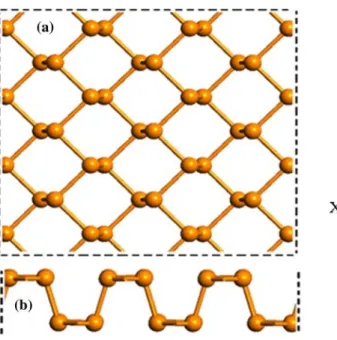
Figure 1 shows the top and the side views of monolayer BP used in the calculations. The BP has two different edges corresponding to zigzag and armchair edges, just like the graphene.
3. Results and discussion
Table 1 shows the lattice parameters of BP for both the numerical and the experi-mental studies. The calculations have been performed for lattice parameters close to experimental and theoretical lattice parameters.
(1) Eb =E dop tot −Eatom (2) Ef=E dop tot − [
Epristinetot + 𝜇dop− 𝜇P
]
(3) Eatom=n𝜇P +m𝜇dop
Figure 1. (colour online) (a) The top and (b) the side views of monolayer BP.
Table 1. lattice parameters of BP for both numerical and experimental studies.
Parameters Present study Numerical study [21] Experimental study [8]
a (Å) 3.31 3.35 3.31
c (Å) 4.38 4.62 4.38
In Table 2, Eb and Ef are calculated by means of Equations (1)–(3). When the comparison is made between the structures with impurities, it is seen that Sn doping has the lowest Eb and Ef values. Therefore, this doping state is energetically the most stable among the other doping states.
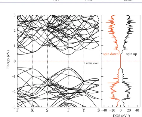
Figure 2 shows the band structure and the DOS of BP had direct band gap at gamma (Γ) point. The bandgap value is 0.85 eV and this result is similar to the previous results [12, 13].
The maximum point of the valence band and the minimum point of the conduc-tion band are in −0.42 and 0.43 eV with respect to Fermi Level, respectively. The Fermi level is located at nearly mid-point the between these bands. As expected, and shown in the DOS calculations, it is shown that there are no spin-dependent states.
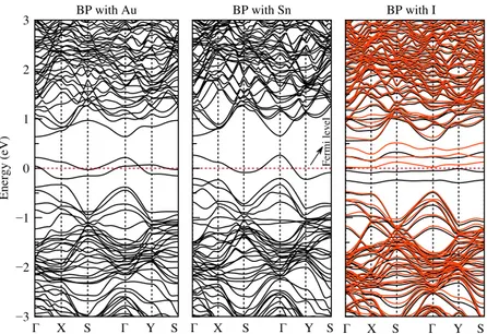
Figure 3 shows band structure of the BP doped with Au, Sn and I atoms. It is shown that the BP doped with Au and Sn atoms has been exhibited metallic behaviour which is independent of spin states. The Fermi level has been entered to the valence band. An impurity band is shown at the Fermi level due to Sn atom. In BP doped with I, it is shown that the band structure is spin-dependent.
Table 2. Ef, Eb and Etot values of BP doped with au, sn, i atoms.
Doping Atoms Ef (eV) Eb (eV) Etot per atom (eV)
au 6.70 −11.75 −279.70 sn −0.36 −18.81 −271.73 i 7.04 −11.42 −265.27 3 2 1 0 1 2 3 Energy (eV) 40 20 0 20 40 DOS (eV-1)
spin down spin up
X S Y S
Fermi level
Figure 2. (colour online) The band structure and the Dos of black phosphorus. note: Red and black lines are represented spin down and spin up states, respectively.
PHILOSOPHICAL MAGAZINE 159
Furthermore, there is nearly spin gapless semiconductor behaviour which has 32 meV of the bandgap in the BP doped with I. With I doping, the BP appears to have an indirect band gap for both spin up and spin down states between X and Γ points. These results are shown that the electronic band structure strongly depends on the specific doping type such as Au, Sn and I.
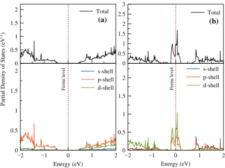
Figure 4(a) shows the partial density of states (PDOS) of a phosphorus (P) atom in the pure structure. The contributions from the shells of atoms contributing to total DOS are clearly visible. In pure structure, p and d shells of P atom formed the conduction band, but only p shell contributed to the valence band. In Au doping state, a charge density is shown at Fermi level. The source of these charge densities is found to be p and d shells. It is shown that the charge density from d shell of Au atom is higher than that of p shell at Fermi level. In contrary to pure structure, while s and p shells of Au atom contribute to the conduction band, d shell contributes to valence bands at near Fermi level, respectively.
Figure 5 shows PDOS of BP with Sn and I doping. It is shown that BP with Sn has a charge density at Fermi level which can be seen in Figure 5(a). As shown, this charge density results from s and p shells of Sn atom. PDOS of BP with I doping atom is shown in Figure 5(b). It is clearly observed that the BP with I doping atom depends on spin states. There are mutual spin states too close to the Fermi level. This may be important in order to control spintronic properties of BP. Previous studies are shown spin dependent for different doping atoms [22, 23]. In Figure
5(b), It can be seen that the source of these spin states mostly is p shell of I atom. Additionally, when compared with Au and Sn doping atoms, BP with I doping has a high charge density near Fermi level.
For a crystal dielectric function (εi,j(ω)) is given by Equation (4):
3 2 1 0 1 2 3 Energy (eV) S X Y S X S Y S X S Y S
BP with Au BP with Sn BP with I
Fermi leve
l
𝜀1(𝜔) is the real part of the dielectric function, while ɛ2(ω) is the imaginary part
of the dielectric function. The optical properties of the BP have been calculated (4) 𝜀i,j(𝜔) = 𝜀1(𝜔) +i𝜀2(𝜔) 0 0.5 1 1.5 2 2.5 3 Total 2 0 0.5 1 1.5 2 Energy (eV) s-shell p-shell d-shell 0 0.5 1 1.5 2
Partial Density of States (e
V -1) Total 2 1 0 1 2 1 0 1 2 0 0.5 1 1.5 2 Energy (eV) s-shell p-shell d-shell (b) (a) Fermi level Fermi level
Figure 4. (colour online) PDos for (a) pure BP and (b) BP with au.
5 0 5 10 spin up spin down 2 1 0 1 2 5 0 5 10 Energy (eV) s-shell p-shell d-shell 0 1 2 3 4
Partial Density of States (e
V -1) Total 2 1 0 1 2 0 0.5 1 1.5 2 2.5 3 Energy (eV) s-shell p-shell d-shell (b) (a) Fermi leve l Fermi leve l Total
Figure 5. (colour online) PDos for (a) BP with sn and (b) BP with i. note: Dashed lines are represented spin down states.
PHILOSOPHICAL MAGAZINE 161
between 0 and 5 eV photon energy values. To analyse the optical properties of the pure BP and BP doped with Au, Sn and I structures, well-known Kramers–Kronig equations (Equations (5) and (6)) were used [32]:
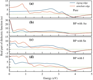
Figure 6 shows real part of dielectric function depending on photon energy for pure and doped BPs. Due to the different edges, it is expected that the different optical properties are exhibited. Thus, it is shown that there are anisotropic optical properties in the zigzag and the armchair edges. For each state, the static dielectric constants have been calculated with Equations (5) and (6). For different edges, different static dielectric constants have been determined and shown in Table 3. (5) 𝜀1(𝜔) =1 + 2 𝜋 𝛿 ∞ ∫ 0 𝜔𝜀2(𝜔) 𝜔 �2 − 𝜔2d𝜔 � (6) 𝜀2(𝜔) = e2h 𝜋n2𝜔2 ∑ ∑ ∫|| | ePif| | | 2 𝛿(EfK−EiK− ℏ𝜔)d3k 0 5 10 15 zigzag edge armchair edge 0 10 20 30
Real part of dielectric function
( ) 5 0 5 10 15 0 1 2 3 4 5 0 5 10 Energy (eV) Pure BP with Au BP with Sn BP with I (a) (b) (c) (d)
Figure 6. (colour online) The changes in the real part of the dielectric function depending on the energy for (a) pure BP crystal and for BP crystal doped with (b) au, (c) sn and (d) i.
Table 3. static dielectric constant and optical band gap values of BP with pure and au, sn and i. #States
Static dielectric constant Optical band gap (eV)
Zigzag Armchair Zigzag Armchair
Pure BP 3.06 7.47 2.75 0.90
BP with au 30.1 30.1 – –
BP with sn 6.44 8.66 0.40 0.45
BP state which has the highest dielectric constant among the studied doping state is Au-doped BP with a value of ~30.1 for both edges.
The imaginary part of the dielectric function depending on photon energy of the studied states are shown in Figure 7. The optical band gaps of each state have been calculated and are shown Table 3. The lower photon energies of BP doped with Au have been shown higher peaks than the others and thus it is expected that these energy values are a high absorption region.
4. Conclusion
In this study, the electronic and the optical properties of BP doped with Au, Sn and I have been investigated by DFT method. The band gap of the BP has been obtained consistent with the literature. The doping atoms have substantially changed the electronic and the optical properties of the BP. In the band structure calculations, BP doped with Au and Sn has exhibited metallic owing to important deep levels in the vicinity of the Fermi level. There are no any spin-dependent states in the BP doped with Au and Sn atoms. However, BP doped with I is found to be spin-dependent. It is determined that energetically the most stable structure is BP with Sn among the doping states others. Because of different edge states, the optical properties of BP have been shown the differences for both edges. The opti-cal properties of each doping states have been investigated and it is determined that BP doped with Au has exhibited a high-static dielectric constant and has shown a high absorption in the low energy regions. These doping atoms may play the important role the controlling of the electronic and the optical properties of BP.
0 5 10 15 zigzag edge armchair edge 0 5 10 15 20 25
Imaginary part of dielectric function
( ) 0 5 10 15 0 1 2 3 4 5 0 5 10 15 Energy (eV) Pure BP with Au BP with Sn BP with I (a) (b) (c) (d)
Figure 7. (colour online) The changes in the imaginary part of the dielectric function depending on the energy for (a) pure BP crystal, and for BP crystal doped with (b) au (c) sn and (d) i.
PHILOSOPHICAL MAGAZINE 163 Acknowledgements
One of the authors (Ekmel Ozbay) also acknowledges partial support from the Turkish Academy of Sciences.
Disclosure statement
No potential conflict of interest was reported by the authors.
Funding
This work is supported by the projects DPT-HAMIT, DPT-FOTON, and NATO-SET-193 and TUBITAK under the project Nos. 113E331, 109A015 and 109E301. This research was sup-ported in part by the Distinguished Young Scientist Award of Turkish Academy of Sciences (TUBA-GEBIP 2016).
References
[1] K.S. Novoselov, A.K. Geim, S.V. Morozov, D. Jiang, Y. Zhang, S.V. Dubonos, and A.A. Firsov, Electric field effect in atomically thin carbon films, Science. 306 (2004), pp. 666–669.
[2] W. Zhao, Z. Ghorannevis, L. Chu, M. Toh, C. Kloc, P.H. Tan, and G. Eda, Evolution of electronic structure in atomically thin sheets of WS2 and WSe, ACS Nano. 7 (2012), pp. 791–797.
[3] H. Shi, R. Yan, S. Bertolazzi, J. Brivio, B. Gao, A. Kis, and L. Huang, Exciton dynamics in suspended monolayer and few-layer MoS2 2D crystals, ACS Nano. 7 (2013), pp. 1072–1080. [4] D. Pacile, J.C. Meyer, Ç.Ö. Girit, and A. Zettl, The two-dimensional phase of boron
nitride: Few-atomic-layer sheets and suspended membranes, Appl. Phys. Lett. 92 (2008), pp. (133107) 1–3.
[5] Q.H. Wang, K. Kalantar-Zadeh, A. Kis, J.N. Coleman, and M.S. Strano, Electronics and optoelectronics of two-dimensional transition metal dichalcogenides, Nat. Nanotechnol. 7 (2012), pp. 699–712.
[6] H.O. Churchill and P. Jarillo-Herrero, Two-dimensional crystals: Phosphorus joins the family, Nat. Nanotechnol. 9 (2014), p. 330.
[7] L. Li, G.J. Ye, V. Tran, R. Fei, G. Chen, H. Wang, and X.H. Chen, Quantum oscillations in a two-dimensional electron gas in black phosphorus thin films, Nat. Nanotechnol. 10 (2015), pp. 608–613.
[8] Y. Maruyama, S. Suzuki, K. Kobayashi, and S. Tanuma, Synthesis and some properties of black phosphorus single crystals, Physica B+ C 105 (1981), pp. 99–102.
[9] G. Fiori, S. Bruzzone, and G. Iannaccone, Very large current modulation in vertical heterostructure graphene/hBN transistors, IEEE Trans. Electron Dev. 60 (2013), pp. 268–273.
[10] D.S. Abergel, J.R. Wallbank, X. Chen, M. Mucha-Kruczyński, and V.I. Fal’ko, Infrared absorption by graphene–hBN heterostructures, New J. Phys. 15 (2013), pp. (123009) 1–7. [11] J. Park, J. Lee, L. Liu, K.W. Clark, C. Durand, C. Park, and G. Gu, Spatially resolved one-dimensional boundary states in graphene–hexagonal boron nitride planar heterostructures, Nat. Commun. 5 (2014), pp. 1–6.
[12] V. Tran, R. Soklaski, Y. Liang, and L. Yang, Layer-controlled band gap and anisotropic excitons in few-layer black phosphorus, Phys. Rev. B 89 (2014), pp. (235319) 1–6.
[13] Y. Du, C. Ouyang, S. Shi, and M. Lei, Ab initio studies on atomic and electronic structures of black phosphorus, J. Appl. Phys. 107 (2010), pp. (093718) 1–4.
[14] A.S. Rodin, A. Carvalho, and A.C. Neto, Strain-induced gap modification in black phosphorus, Phys. Rev. Lett. 112 (2014), pp. (176801) 1–5.
[15] S. Endo, Y. Akahama, S.I. Terada, and S.I. Narita, Growth of large single crystals of black phosphorus under high pressure, Jpn. J. Appl. Phys. 21 (1982), pp. L482–L484.
[16] H. Liu, Y. Du, Y. Deng, and D.Y. Peide, Semiconducting black phosphorus: Synthesis, transport properties and electronic applications, Chem. Soc. Rev. 44 (2015), pp. 2732–2743. [17] M. Köpf, N. Eckstein, D. Pfister, C. Grotz, I. Krüger, M. Greiwe, and T. Hansen, Access and
in situ growth of phosphorene-precursor black phosphorus, J. Cryst. Growth 405 (2014), pp. 6–10.
[18] M. Zhao, X. Niu, L. Guan, H. Qian, W. Wang, J. Sha, and Y. Wang, Understanding the growth of black phosphorus crystals, Cryst. Eng. Comm. 18 (2016), pp. 7737–7744. [19] M. Zhao, H. Qian, X. Niu, W. Wang, L. Guan, J. Sha, and Y. Wang, Growth mechanism
and enhanced yield of black phosphorus microribbons, Cryst. Growth Des. 16 (2016), pp. 1096–1103.
[20] T. Nilges, M. Kersting, and T. Pfeifer, A fast low-pressure transport route to large black phosphorus single crystals, J. Solid State Chem. 181 (2008), pp. 1707–1711.
[21] S. Lange, P. Schmidt, and T. Nilges, Au3SnP7@ black phosphorus: An easy access to black phosphorus, Inorganic Chemistry 46 (2007), pp. 4028–4035.
[22] T. Hu and J. Hong, First-principles study of metal adatom adsorption on black phosphorene, J. Phys. Chem. C 119 (2015), pp. 8199–8207.
[23] W. Yu, Z. Zhu, C.Y. Niu, C. Li, J.H. Cho, and Y. Jia, Dilute magnetic semiconductor and half-metal behaviors in 3d transition-metal doped black and blue phosphorenes: a first-principles study, Nanoscale Res Lett. 11 (2016), pp. 1–9.
[24] X.B. Li, P. Guo, T.F. Cao, H. Liu, W.M. Lau, and L.M. Liu, Structures, stabilities, and electronic properties of defects in monolayer black phosphorus, Sci. Reports 5 (2015), pp. 1–11.
[25] Version 2016.4 QuantumWise A/S. Available at http://www.quantumwise.com. [26] M. Brandbyge, J.L. Mozos, P. Ordejón, J. Taylor, and K. Stokbro, Density-functional method
for nonequilibrium electron transport, Phys. Rev. B 65 (2002), p. B864.
[27] J.M. Soler, E. Artacho, J.D. Gale, A. García, J. Junquera, P. Ordejón, and D. Sánchez-Portal, The SIESTA method for Ab initio order-N materials simulation, J. Phys. Condens. Matter. 14 (2002), pp. 2745–2779.
[28] J.P. Perdew, K. Burke, and M. Ernzerhof, Generalized gradient approximation made simple, Phys. Rev. Lett. 77 (1996), pp. 3865–3868.
[29] E. Kutlu, P. Narin, G. Atmaca, B. Sarikavak-Lisesivdin, S.B. Lisesivdin, and E. ÿzbay, Effect of substitutional As impurity on electrical and optical properties of β-Si 3 N 4 structure, Mater. Res. Bull. 83 (2016), pp. 128–134.
[30] B. Sarikavak-Lisesivdin, S.B. Lisesivdin, and E. Ozbay, Ab initio study of Ru-terminated and Ru-doped armchair graphene nanoribbons, Mol. Phys. 110 (2012), pp. 2295–2300. [31] E. Kutlu, P. Narin, B. Sarikavak-Lisesivdin, S.B. Lisesivdin, and E. Ozbay, Electronic
properties of Li-doped zigzag graphene nanoribbons, Physica E. 84 (2016), pp. 543–547. [32] Y. Du, B. Chang, X. Fu, X. Wang, and M. Wang, Electronic structure and optical properties