Electronic and magnetic properties of graphane nanoribbons
H. Şahin,1 C. Ataca,1,2and S. Ciraci1,2,
*
1UNAM-Institute of Materials Science and Nanotechnology, Bilkent University, 06800 Ankara, Turkey 2Department of Physics, Bilkent University, 06800 Ankara, Turkey
共Received 27 January 2010; revised manuscript received 26 April 2010; published 12 May 2010兲
In this study, we investigate the electronic and magnetic properties of graphane nanoribbons. We find that zigzag and armchair graphane nanoribbons with H-passivated edges are nonmagnetic semiconductors. While bare armchair nanoribbons are also nonmagnetic, adjacent dangling bonds of bare zigzag nanoribbons have antiferromagnetic ordering at the same edge. Band gaps of the H-passivated zigzag and armchair nanoribbons exponentially depend on their width. Detailed analysis of adsorption of C, O, Si, Ti, V, Fe, Ge, and Pt atoms on the graphane ribbon surface reveal that functionalization of graphane nanoribbons is possible via these adatoms. It is found that C, O, V, and Pt atoms have tendency to replace H atoms of graphane. We showed that significant spin polarizations in graphane can be achieved through creation of domains of H vacancies and CH divacancies.
DOI:10.1103/PhysRevB.81.205417 PACS number共s兲: 73.22.Pr, 75.75.⫺c, 61.48.⫺c, 62.23.Kn
I. INTRODUCTION
After the synthesis of two-dimensional 共2D兲 graphene,1–6
its nanoribbons 共NRs兲 have been a subject of interest, both experimentally7,8 and theoretically.9–15 Advances in
experi-mental techniques are paving the way for integrating the ex-ceptional electrical, optical, and magnetic functionalities of these nanometer-sized materials into future electronic tech-nology. In addition to numerous theoretical and experimental works on graphene and its NRs, research efforts have been also devoted to synthesize its various derivatives. Notably, the synthesis of a 2D hydrocarbon in honeycomb structure,16
namely, graphane, followed its prediction through theoretical works.17,18 Detailed analysis of hydrogenation processes of
graphene leading to graphane and the existence of hydrogen 共H兲 frustrations were discussed very recently.19Furthermore,
it was reported that graphane NRs have more favorable for-mation energies than experimentally available graphene ribbons.20 Recently, we reported the possibility of obtaining
magnetization through dehydrogenation of domains on 2D graphane.21Modification of electronic structure of graphane by introducing either a hydroxyl group or a H vacancy was also investigated with GW self-energy calculations.22
Al-though there are several recent studies on graphane, electri-cal and magnetic properties of its NRs have remained unex-plored.
Recent advances in graphane have motivated us to ex-plore the properties of zigzag and armchair graphane NRs. In this paper, using first-principles plane-wave method within the density-functional theory共DFT兲 we investigated the elec-tronic and magnetic properties of bare and H-passivated graphane NRs. We also explored the effects of specific im-perfections on these properties. These are various foreign atoms adsorbed on the surfaces of graphane NRs, vacancies, and edge roughness. We found that these imperfections can attribute interesting functionalities by modifying the elec-tronic and magnetic properties of graphane NRs.
II. METHODS
We perform first-principles calculations23within DFT
us-ing projector augmented wave potentials24 and approximate
exchange-correlation functional by spin-polarized local-density approximation25 共LDA兲. Kinetic energy cutoff ប2兩k + G兩2/2m for plane-wave basis set is taken as 500 eV. In the self-consistent potential and total-energy calculations of 2D graphane, a set of共35⫻35⫻1兲 k-point sampling is used for Brillouin-zone 共BZ兲 integration. The convergence criterion of self-consistent calculations for ionic relaxations is 10−5 eV between two consecutive steps. By using the conjugate-gradient method, all atomic positions and unit cells are optimized until the atomic forces are less than 0.03 eV/Å. Pressures on the lattice unit cell are decreased to values less than 1.0 kbar.
In order to correct the energy bands and band-gap values obtained by LDA, frequency-dependent GW0 calculations are carried out.26 Screened Coulomb potential W, is kept
fixed at initial DFT value W0 and Green’s function G, is iterated five times. GW0 self-energy calculations are carried out with 15 Å vacuum spacing, default cutoff potential, 160 bands, and 64 grid points.
Graphane NRs are treated by the supercell geometry within periodic boundary conditions. Vacuum spacing of at least 15 Å is placed between adjacent graphane NRs to hinder the interactions. In specific cases double unit cell is used in our calculations to allow the possible antiferromag-netic 共AFM兲 orderings along the ribbon edges. Reciprocal space integrations are carried out with 1⫻1⫻15 Monkhorst-Pack k-point grids.
III. TWO-DIMENSIONAL GRAPHANE
For a better understanding of graphane NRs we start with 2D graphane which is derived from the hydrogenation of graphene, where each carbon atom is saturated by a single hydrogen atom. Accordingly, the primitive cell of graphane consists of two carbon and two hydrogen atoms. Chairlike configuration of infinite sheet of 2D graphane is formed, whereby each carbon atoms of A- and B-type sublattices are saturated by hydrogen atoms from above and below, respec-tively, as described in Fig. 1共a兲. This is known as the most favorable and stable hydrocarbon conformation.17,21The
pla-nar graphene honeycomb structure, which is stabilized by planar sp2-hybrid orbitals and bonding between adjacent perpendicular pzorbitals is puckered共buckled兲 as a result of the adsorption of H atoms, whereby a single C atom is bound to three adjacent C atoms and a single H atom through “tet-rahedrally coordinated” sp3-like hybrid orbitals. The buck-ling, ␦, i.e., the perpendicular distance between A-type and B-type carbon sublattices, is calculated to be 0.45 Å. As a result, the lattice constant of graphene increases from 2.46 to 2.51 Å and hence the C-C and C-H bond lengths become 1.52 Å and 1.12 Å, respectively, as indicated in Fig. 1共a兲. The charge-density contour plots given in Fig.1共b兲 indicate that the charge distribution in graphane especially around the C-C bond is reminiscent of that in tetrahedrally coordinated diamond. In graphane, the angle H between H-C and C-C bonds andC between adjacent C-C bonds are 107.35° and
111.51°, respectively. The mean value of these angles is equal to the tetrahedral angle Cof diamond. The maximum of the C-C bond charge in diamond and in graphane are found to be⬃0.282 e/Å3 and⬃0.286 e/Å3, respectively.
The cohesive energy of graphane共per unit cell兲 relative to free C and H atoms is obtained from Ec= 2⫻ET
H + 2⫻ET
C − ET
Gra
, where ETHand ETCare the total energies of single free C and free H, whereas ET
Gra
is the total energy of graphane. The cohesive energy depends whether the energies of mag-netic or nonmagmag-netic共NM兲 states of free C and free H atoms are considered. Here the cohesive energy per unit cell of graphane is calculated to be 23.57共27.65兲 eV by considering the magnetic 共nonmagnetic兲 states of free atoms. As for the average C-H bond energy, one can use the formula EC-H= 共−ET
Gra
+ ETGre+ 2⫻ETH兲/2, where ETGre is the total energy of graphene. The calculated value is 2.84共3.74 for nonmagnetic case兲. We reported21 that the desorption of a single H atom
from the graphane is an endothermic reaction with an energy of 4.79 eV. When compared with the energy of C-H bond, the desorption energy of single H is larger since the single H removal creates reconstruction of nearby atoms which fur-ther reduces the total energy of the system.
Due to sp3 saturation of C atoms, 2D graphane is a NM semiconductor with a direct band gap of 3.42 eV as shown in Fig. 1共c兲. However, this band gap, which is underestimated within DFT, is corrected by GW0approximation to become 5.97 eV.21,22 While the top of the valence band originates
from pxand pyorbitals of C atoms, the bottom of the con-duction band has C pz orbital character. Earlier, we also calculate21the phonon modes of infinite 2D graphane, which
yield all real frequencies in BZ. Having all frequencies posi-tive indicate the stability of graphane structure.
An exceptional feature of graphane is related with its in-teresting charging configuration. While graphene has a cova-lent bonding, upon the saturation of each C atom by a single H atom, a charge of␦Q⬃0.1 electrons is transferred from H to C. At the end, the negatively charged bilayer of carbon atoms becomes sandwiched between positively charged H layers. Graphane having this charging has the photoelectric threshold 共work function兲 calculated to be ⌽=4.97 eV, which is 0.2 eV larger than that of graphene. In TableI, we presented the calculated values related with structure, energy bands, photoelectric threshold, etc., of graphane and graphene for the sake of comparison. To be complete TableI also includes calculated elastic constants such as in-plane stiffness27 C 关=1
A共 2E
T
⑀2兲, where ET is the total energy of the system under strain,⑀is the uniaxial strain, and A is the area of the unit cell兴 and Poisson’s ratio28.
IV. GRAPHANE NANORIBBONS
The nanoribbons cut from a 2D graphane are structures providing important features for various technological appli-cations. Two major families of graphane NRs are distin-guished depending on their orientations, namely, armchair and zigzag graphane NRs. Apart from the orientation, graphane NRs are characterized by their widths. For arm-chair graphane NRs, the width, N, is defined by the number of C-C dimers in the unit cell which are parallel to the axis of b dC-C=1.52A 1 o A B (c) ) (b M K Γ K (a) b2 dC-H=1.12A o δ=0.45 Ao C C H H C C C C
θ
Cθ
Cθ
H Diamond Structure Graphane Structure -10 0 10Energy
(eV)
pz px p +sz py s EFFIG. 1. 共Color online兲 共a兲 Top and perspective view of the atomic structure of infinite 2D graphane sheet having honeycomb structure. Two sublattices of graphane are indicated by A and B. Black 共dark兲 and blue 共light兲 balls are for carbon and hydrogen atoms, respectively. 共b兲 Charge density contour plots of diamond and graphane are shown on a plane passing through C-C-C-C and H-C-C-H bonds, respectively. The tetrahedral angle of the diamond C= 109.47°. Arrows indicate the direction of increasing charge
density. The calculated values of C and H, namely, C-C-C and H-C-C bond angles in graphane, respectively, are given in TableI. Contour spacings are 0.0286 e/Å3. 共c兲 The LDA energy-band
structure where the orbital character of specific bands is also given. The band gap is shaded yellow/gray.
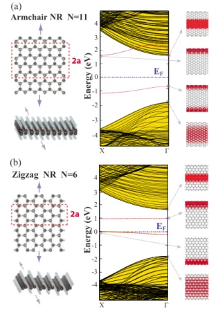
the nanoribbon; for zigzag graphane NRs, N denotes the number of zigzag carbon chains along the nanoribbon axis. The electronic structure changes depending on whether the dangling bonds of carbon atoms at the edge are free共bare兲 or passivated by single H atoms. In Figs.2共a兲and2共b兲we show the atomic and electronic structure of armchair and zigzag graphane NRs with N = 11 and N = 6, respectively.
Bare armchair graphane NR is a NM indirect band-gap semiconductor since the electrons at the dangling orbitals are paired. The band gap of 2D graphane is reduced due to the bands of edge states of dangling bonds occurring in the band gap. The charge-density analysis of these edge state bands presented in Fig.2共a兲clearly shows that they are localized at the edges of the NR. Upon hydrogen passivation of the three-fold coordinated edge atoms, the edge state bands in the gap disappear and the direct band gap opens up.
Similar to armchair graphane NRs, the dangling bonds of the threefold coordinated carbon atoms at both edges of zig-zag graphane NRs give rise to edge states in the band gap. Owing to relatively large distance between adjacent dangling bonds and hence their relatively smaller coupling, they have a minute dispersion. Charge density isosurfaces of these edge states confirm their localization at the edges. Also, owing to their weak coupling the spins of adjacent dangling bonds cannot be paired. Consequently, each carbon atom at the zig-zag edge attains a magnetic moment of 1 Bohr magneton 共B兲. The ordering of these magnetic moments is however dramatically different from that of the zigzag graphene NRs. The significant coupling between two spin states at different edges gives rise to AFM ordering along the graphene edge.
The physical origin of the magnetic interactions between the edges of graphitic fragments was treated earlier.9 For
zigzag graphene nanoribbon, collective alignment of the magnetic moments is along the same ribbon edge through the ferromagnetic 共FM兲 interaction but AFM ordering between opposite edges is attributed to magnetic-tail interactions. The magnetic ordering of a wide zigzag graphane NRs 共⬃2 nm兲 are examined in a supercell comprising two unit cells, whereby antiferromagnetic ordering between adjacent dangling bonds at the same edge is allowed. We consider four different orderings, such as AFM-AFM共where, respec-tively, the ordering of magnetic moments at the atoms lo-cated at different and same edge are antiferromagnetic兲, FM-AFM, AFM-FM, and FM-FM as described in Fig. 3. Here the difference charge density is defined as the ⌬=共↑兲 −共↓兲, where ↑共↓兲 is spin-up 共spin-down兲 charge. Since the
magnetic interaction between two edges vanishes, AFM-AFM and FM-AFM-AFM orderings have the same total energy corresponding to the ground state. These orderings are 125 meV energetically more favorable than the AFM-FM and
(a) Energy (eV) Γ X EF 1 2 3 4 -4 0 -1 -2 -3 Γ X E ArmchairNR N=11 F Energy (eV) 1 2 3 4 0 -1 -2 -3 -4 2a 2a (b) Zigzag NR N=6
FIG. 2. 共Color online兲 共a兲 Atomic structure of bare armchair graphane NR having N = 11. The double unit cell of the nanoribbon is delineated by red/dashed lines with the lattice constant 2a. Large/ black and small/light blue balls indicate carbon and hydrogen at-oms. Energy-band structure corresponding to the armchair graphane NR and charge density of selected bands are shown in the panels at the righthand side.共b兲 Atomic structure of bare zigzag graphane NR having N = 6 with double unit cell delineated by red/dashed lines and with lattice constant 2a. Energy-band structure and isosurface charge density of selected states corresponding to zigzag graphane NR are indicated. Bands shown by red/dotted lines are derived from edge states. Zero of energy is set to the Fermi level, shown by dashed-dotted lines, of the nanoribbons with H-passivated edges. In spin polarized calculations double unit cell is used to allow antifer-romagnetic order along the edges.
TABLE I. Comparison of the calculated quantities of graphene and graphane. Lattice constant, a; C-C bond distance, dC-C; C-H bond
distance, dC-H; the buckling,␦关see Fig.1共a兲兴; angle between adjacent C-C bonds,C关see Fig.1共b兲兴; angle between adjacent C-H and C-C
bonds,H; energy band gap calculated by LDA, EgLDA; energy band gap corrected by GW0, EGWg 0; cohesive energy EcNM,共Ecm兲 obtained with
respect to nonmagnetic共magnetic兲 free-atom energies; the C-H bond energy, EC-HNM共EC-Hm 兲 obtained with respect to nonmagnetic 共magnetic兲 free-atom energies; photoelectric threshold共work function兲, ⌽; in-plane stiffness, C and Poison ratio,.
Material共1⫻1兲 unit cell a 共Å兲 dC-C 共Å兲 dC-H 共Å兲 共Å兲␦ 共deg兲C 共deg兲H EgLDA 共eV兲 EgGW0 共eV兲 EcNM 共eV兲 Ecm 共eV兲 EC-HNM 共eV兲 EC-Hm 共eV兲 共eV兲⌽ C 共J/m2兲 Graphene 2.46 1.42 120 0.00 0.00 20.16 17.87 4.77 335a 0.16 Graphane 2.51 1.52 1.12 0.45 111.51 107.35 3.42 5.97 27.65 23.57 3.74 2.84 4.97 243b 0.07 aReference29. bReference30.
FM-FM orderings. From this analysis it is revealed that AFM spin alignment between adjacent atoms at the same edge is preferred by the zigzag graphane NRs. FM ordering between two spins has 62.5 meV higher energy. For zigzag graphane NR with N = 6, the magnetic coupling between two edges is negligible and hence either AFM-AFM or FM-AFM order-ings have the same energy and they are ground states. How-ever, when the width of the nanoribbon is less than 12 Å the degeneracy of AFM-AFM and FM-AFM states is broken. The bare zigzag graphane NR is an indirect and antiferro-magnetic semiconductor with an indirect band gap relatively smaller than that of 2D graphane. However, it becomes NM, direct band-gap semiconductor upon passivation of the dan-gling bonds. Also the magnetic edge states disappear and band gap becomes larger.
The value of the band gap of graphane NRs can differ from that of parent 2D structure due to a combined effects of quantum confinement, edge state bands as well as folding in the direction perpendicular to the NR axis. We note that the band gap of graphane NR depends on its width given by N. However, the quantum confinement effect is not as empha-sized as that found in graphene NR. In Fig.4, H-passivated armchair and zigzag graphane NRs display a quantum con-finement effect, namely, the band-gap reduction with increas-ing width or N. This behavior is fitted to an expression as
Egap共N兲 = 3.42 eV +␣exp共− N兲. 共1兲 Here␣ andare fitting parameters. The values of␣and are found to be 1.18 and 0.19 eV for zigzag graphane NRs
共2.15 and 0.14 eV for armchair graphane NRs兲. The band gaps of both types of graphane NRs go to 3.42 eV as N →⬁. Considering the GW0corrected value of the band gap, 5.97 eV, the above fitting can be expressed as Egap共N兲 = 5.97+␣exp共−N兲 assuming that the same scissor opera-tion is applicable for graphane NRs. Apparently, the band-gap values of graphane NRs calculated using DFT are under-estimated and hence their values are expected to occur ⬃2.5 eV larger than presented in Fig.4. Unfortunately, GW0 self-energy corrections cannot be performed for graphane NRs due to large computational time. We note that the varia-tion in band gap is relevant for N⬍22 for zigzag graphane NRs and N⬍30 for armchair graphane NRs. In Ref.20the band gaps of hydrogen saturated graphane NRs were calcu-lated for 6ⱕNⱕ15 using generalized gradient approxima-tion共GGA兲. In the present study band gaps are calculated for 10ⱕNⱕ40 using LDA. The hydrogenated graphane NRs included in both studies, namely, those 10ⱕNⱕ15 are in good agreement. Largest band-gap difference of 0.1 eV found between two studies is attributed to different approxi-mations 共i.e., LDA versus GGA兲 in representing exchange-correlation potential.
V. FUNCTIONALIZATION OF GRAPHANE NRs BY ADATOMS
Adsorption of adatoms is widely used and an efficient way to provide new functionalities to structures in nanoscale applications.31–33Adsorption of C, O, Si, Ge, Pt, V, Fe, and
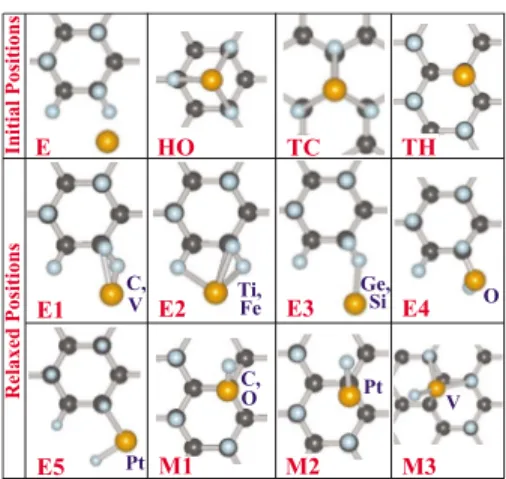
Ti adatoms on graphane nanoribbons is investigated by using 共1⫻1⫻6兲 supercell of H-passivated armchair graphane NR having N = 8. Adsorption geometry is determined by calcu-lating the lowest binding energy corresponding to the opti-mized structures. To this end, the binding energies of ada-toms at four initial sites described in Fig. 5: these are edge site E, hollow site HO, top site of the carbon TC, and top site of the hydrogen atom TH in the middle of NR. The stable binding sites are determined upon structure relaxation. In the
FM-FM AFM-AFM ∆E = 0.125 E = 0 FM-AFM E = 0 AFM-FM ∆E = 0.125
FIG. 3. 共Color online兲 Total energies of possible magnetic or-derings at the edges of bare zigzag graphane nanoribbons. Calcula-tions are performed in double unit cell delineated by red/dashed lines. Spin-up and spin-down states are shown by green/dark and gray/light isosurfaces of the difference charge density,⌬.
10 20 30 40 3.4 3.5 3.6 3.7 3.8 10 20 30 40
Band
G
ap
(eV
)
Ribbon Width (N)
Zigzag NR
Armchair NR
FIG. 4. 共Color online兲 Variation in the energy band gap of H-passivated zigzag and armchair NRs of graphane as a function of width given by N. The variation in the band gap with N is fitted to the curve given by continuous line.共See text.兲
E HO Initial Positions Relaxed Positions E1 E3 E4 E5 E2 M1 M2 M3 C, Fe Ge, O Pt Si Ti, V C, O Pt V TC TH
FIG. 5.共Color online兲 Schematic representations of possible po-sitions of adatoms on a large H-passivated armchair graphane nan-oribbon. Positions of adatoms obtained after the structure optimiza-tion through minimizaoptimiza-tion of total energy and forces exerting on the atoms are also shown.
same figure the positions of adatoms after relaxation are also shown. Binding energies共Eb兲 of these atoms are calculated by using the expression
Eb= − ET关NR + A兴 + ET关NR兴 + ET关A兴 共2兲 in terms of the total energies of the optimized structure of graphane NR with adatom, ET关NR+A兴; bare NR, ET关NR兴; and free adatom, ET关A兴. Owing to the large graphane nano-ribbon unit cell, k-point sampling is done only along the axis of the ribbon. All the energies are calculated in the same unit cell and obtained from the lowest ground-state total energies 共either magnetic or nonmagnetic兲. Initially, at least 2 Å dis-tance between adatom and outermost graphane atom is pro-vided to find the relaxation site of adatom on the ribbon.
An atom adsorbed on graphane NR may give rise to reso-nance states in the valence and conduction bands, and also localized states in the band gap. Owing to the periodic boundary conditions, the energy levels associated with these adatoms may form energy bands. Since we consider a super-cell consisting of six unit super-cell of H-passivated armchair graphane NR, the adatom-adatom distance is large and pre-vents coupling between adjacent adatoms. In this respect, the flat bands associated with adatoms can mimic either reso-nance or localized states relevant for dilute doping.
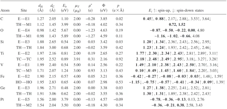
In Table II, we present nearest-neighbor distances be-tween adatom and H 共dH兲 and C 共dC兲, binding energy 共Eb兲, total magnetic moment of the system共T兲, and charge trans-fer between adatom and adsorbate 共ⴱ兲. Since the inversion symmetry of graphane can be broken by the adsorption of an
atom, a net electric dipole moment can be induced thereof. Thus electric dipole moment values calculated in the direc-tion normal to graphane NR surface p, induced by adatom are also listed in Table II. Photoelectric threshold of the adatom+ graphane system perpendicular to the plane of NR, ⌽, is calculated by the difference of the electrostatic poten-tial at distances where the gradient of it is negligible and the Fermi level of the adsorbed system. It should be noted that both p and ⌽ is relevant only for uniform coverage of graphane. For a dilute impurity, these calculated values con-verge to that of armchair graphane. When the width of arm-chair graphane NR is large enough, one expects the photo-electric threshold,⌽, and dipole moment, p, to converge to 4.97 eV and 0 eÅ, respectively.21
We found that some atoms, such as C, O, V, and Pt that are adsorbed on the H-passivated armchair graphane NR sur-face show a tendency to remove H atoms from graphane surface. Since the single atoms of C, O, V, and Pt have rather high binding energy, it seems possible to create graphene domains on graphane by striping H atoms but covering the domain by adsorbed atoms. Independent of their initial posi-tion, C and O atoms are adsorbed to carbon atoms of graphane by replacing H atoms. A typical binding configura-tion of C and O is indicated as M1 in Fig.5. Adsorption of C and O atoms occur at the middle of nanoribbon with strong binding energies of 5.89 eV and 3.99 eV, respectively. The resulting system is NM. Binding structures of Pt and V, which also remove H atom from the host C atom of graphane, are also shown in the same figure.
TABLE II. Summary of the calculated quantities for adatoms adsorbed on a H-passivated armchair graphane NR. The first and second lines in each row associated with a given adatom adsorbed to edge site and the sites near the center of the graphane NRs, respectively. dH, the adatom nearest hydrogen distance; dC, the nearest adatom carbon distance; Eb, adatom binding energy; T, magnetic moment per
supercell;ⴱ, excess charge on the adatom共where negative sign indicates excess electrons兲; ⌽, photoelectric threshold 共work function兲; p, dipole moment calculated in the direction normal to graphane NR surface; Eienergies of localized states associated with adatoms. Localized
states are measured from the top of the valence bands in electron volt. The occupied ones are indicated by bold numerals and their spin alignments are denoted by either↑ or ↓. Up to first seven adatom states of Eiare shown.
Atom Site dH 共Å兲 dC 共Å兲 Eb 共eV兲 共TB兲 ⴱ 共e兲 共eV兲⌽ p
共e⫻Å兲 Ei↑: spin-up, ↓: spin-down states
C E→E1 1.27 2.05 1.10 2.00 −0.28 3.85 0.02 0 . 45↑, 0.88↑, 2.17↓, 2.88↓, 3.53↑, 3.64↓ TH→M1 1.12 1.45 3.99 0.00 −0.18 4.02 0.34 0.72, 1.52 O E→E4 0.98 1.42 5.67 0.00 −1.23 4.63 0.19 −0 . 87, −0 . 50, −0 . 22, 0.00, 4.80 TH→M1 0.98 1.43 5.89 0.00 −1.27 4.59 0.11 −1 . 16, −1 . 02, −0 . 66, 4.08 Si E→E3 1.88 2.65 0.54 2.00 0.03 3.42 0.03 1 . 20↑ ,1.34↑, 2.36↑, 2.43↓, 2.56↓, 2.95↓ TH→TH 1.84 3.00 0.68 2.00 −0.02 3.59 0.42 1 . 23↑ ,1.24↑, 1.93↑, 2.42↓, 2.45↓, 2.46↓ Ti E→E2 1.97 2.16 0.81 2.00 0.19 2.65 0.27 1 . 77↑ ,2.30↓ ,2.34↑ ,2.43↑, 2.81↑, 2.89↑, 3.11↑ TC→TC 1.95 2.52 0.89 3.91 0.31 2.16 0.92 2 . 18↑ ,2.48↑ ,2.49↑ ,2.95↑, 3.18↓, 3.27↑, 3.28↑ V E→E1 1.99 2.40 0.54 5.00 0.14 2.56 0.22 1 . 49↑ ,2.10↑ ,2.38↑ ,2.43↑ ,2.50↑, 2.70↑, 3.16↓ TC→M3 1.71 2.07 1.24 3.00 0.93 3.13 0.43 0 . 10↑ ,0.49↓ ,1.45↑ ,1.60↑ ,1.84↑, 2.20↑, 3.03↓ Fe E→E2 1.90 2.15 0.57 4.00 0.05 3.21 0.36 −0 . 42↑ ,−0.27↑ ,−0.08↑ ,−0.03↑ ,0.03↑, 1.48↓, 1.59↑ HO→HO 1.95 2.83 0.65 4.00 0.07 2.98 0.53 −1 . 15↓ ,−0.75↑ ,−0.57↑ ,−0.41↑ ,−0.34↑ ,0.09↑, 1.39↑ Ge E→E3 1.96 2.71 0.48 2.00 0.00 3.38 0.03 1 . 27↑ ,1.38↑, 2.25↑, 2.41↓, 2.52↓, 2.81↓ TH→TH 1.91 3.06 0.62 2.00 −0.02 3.55 0.36 1 . 30↑ ,1.31↑, 1.89↑, 2.38↑, 2.42↑, 2.43↑ Pt E→E5 1.56 2.00 3.79 0.00 −0.13 4.57 −0.09 −0 . 78, −0 . 36, −0 . 13, 0.13, 2.76 TH→M2 1.54 2.04 3.50 0.00 −0.18 4.30 0.34 −0 . 36, −0 . 21, 0.38, 2.58, 3.43
Although H has very low binding energy 共and hence is not shown in Table II兲, it may be important for striping H atoms from graphane. Upon all geometry relaxations from different initial conditions, single adsorbed H atom prefers to bind on top of H atom of graphane and forms H2 molecule which is weakly bound to the nearest C atom. The binding energy of H2 molecule is calculated to be⬃36 meV.
VI. VACANCIES IN GRAPHANE NRs
In our recent study,21 we showed that a graphane, which
has a NM ground state, can be made magnetic simply by removing hydrogen atoms from the uniform hydrogen layers adsorbed on its both sides. It was found that the magnetiza-tion depends on whether the defect region is one sided or two sided. It was also shown that in certain circumstances re-markably large magnetic moments can be attained in a small domain on the sheet of graphane. Experimentally, removal of surface hydrogen atoms by using laser beam resonating with surface-atom bond,34 ionic vapor application,35 and
subna-nometer Pt clusters36are reported before. Since it is revealed
that the double-sided vacancies give higher magnetic mo-ments we focus on these type of vacancies on the nanorib-bons.
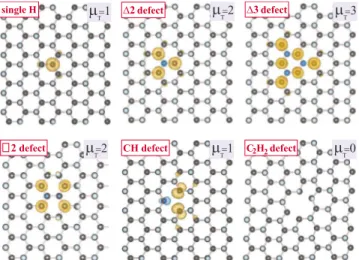
In this section we consider six different types of vacancies in a bare armchair graphane NR with N = 15. Upon desorp-tion of a single hydrogen atom, as shown in Fig. 6, local bonding through sp3-hybrid orbital is retransformed into pla-nar sp2and perpendicular p
zorbitals. At the vacancy site one electron accommodated by the dangling pz orbital becomes unpaired and hence contributes to the magnetization by 1 B. We also calculated that a single H vacancy located at the center of the NR has 70 meV lower energy than that located near the edge of the ribbon.
The situation is rather intriguing for the magnetization of large domains of hydrogen vacancies. As in the case of single H vacancy, leading to transformation of sp3 bonding into planar sp2 bonding, triangular ⌬, and rectangular 䊐 shaped large graphene islands can be created by removing H atoms hence by creating H-vacancy domains. As shown in Fig. 6, hydrogen desorbed triangle-shaped island consisting of n carbon atom at its each edge is defined as ⌬n-type H vacancy. Therefore, a ⌬n-type vacancy domain can be ob-tained by removing n共n+1兲/2 H atom from top side and n共n−1兲/2 H atom from down side of the graphane nanorib-bon. This means that n共n+1兲/2pz-orbital electrons freed from A-type and n共n−1兲/2pz-orbital electrons freed from B-type sublattice C atoms. According to the Lieb’s theorem37
net magnetic moment of such a system can be calculated from the difference between the sublattice atoms. For tri-angle vacancies this difference is simply equal to n and thus the⌬n-vacancy domain has net magnetic moment with nB. However, the 䊐-type domains do not yield large magnetic moments and have values between 0 and 2 B. It is seen that magnetic interactions in double-sided triangular and square H-vacancy domains resulting in net magnetic moments are relatively straightforward and are in good agreement with Lieb’s theorem.
We also consider CH and C2H2vacancies, the synthesis of them are relatively easier than creating only H vacancies. In our study, these vacancies are first created in a NR by remov-ing involved atoms and subsequently their structures are op-timized. Calculated values of magnetic moments of the struc-ture are presented in Fig. 6. After the creation of a CH vacancy on a graphane nanoribbon, geometric structure rear-ranges itself via Jahn-Teller-type distortion in the lattice. Charge-density plot in Fig. 6 shows the unpaired up- and down-spin electron states located on the region surrounding the vacancy. It is seen that a bare armchair graphane NR, which is NM semiconductor when it is defect free, attains permanent magnetic moment in the presence of CH vacan-cies. While CH-type vacancy makes small changes in the geometric structure, Stone-Wales-type deformation occurs after formation of the C2H2 vacancy. Since electrons are paired in C2H2 vacancy, the ground state is again NM and thus there is no visible difference charge density in Fig. 6. From the point view of Lieb’s theorem, removal of a CH couple results in an absence in the number of pz-orbital elec-tron belonging to a A-type 共or B-type兲 sublattice. Upon the creation of C2H2vacancy, both the A- and B-type sublattices lose one electron and thus the difference is zero resulting in a NM ground state. Our results are consistent with the re-cently reported values for CH vacancies in infinite sheets of graphane.38
VII. EDGE ROUGHNESS
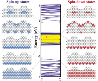
Earlier, it was shown that the edge roughness of graphene NRs can affect their electronic39–41and mechanical42
proper-ties. In particular, it was revealed that periodically repeating edge profiles can be treated within the superlattice structure, which result in confinement of spin states in zigzag NRs.43
Band alignments of these superlattice structures have been µT=1
single H
CH defect
∆2 defect µT=2 ∆3 defect µT=3
2 defect µT=2 µT=1 C H defect2 2 µT=0
FIG. 6.共Color online兲 Atomic structures corresponding to single H, double-sided triangular shaped⌬2 and ⌬3, double-sided rectan-gular shaped䊐2, CH and C2H2vacancies and resulting difference
charge density,⌬=共↑兲−共↓兲, surfaces for a bare armchair graphane NR. Large/black and small/light blue-gray balls indicate C and H atoms, respectively. Only a small part which includes vacancy re-gion and its nearby atoms, of the armchair graphane NR with N = 15 is shown.
studied both experimentally and theoretically.8 Here we
in-vestigated the effect of periodically repeating edge roughness of a bare zigzag graphane NR. While one edge of NR is kept flat, periodically repeating undulations are carved at the other edge. The same structure can be viewed as periodically re-peating heterostructures of wide 共N=8兲 and narrow 共N=6兲 segments of zigzag graphane NRs. Atomic and electronic band structure of this superlattice, which mimics the edge roughness are shown in Fig. 7. Here we note that infinite bare zigzag graphane NR with N = 8 has a band gap of 0.8 eV while the band gap of infinite bare zigzag graphane NR with N = 6 is relatively wider and 0.9 eV. As pointed out in Sec. IV, wide band gap of H-passivated graphane NRs is reduced to 0.8–0.9 eV because of edge states of unpassivated dan-gling bonds of bare graphane NRs, which appear in the band gap. These edge states in Fig.7 of the superlattice occur as several closely lying flat bands below and above the Fermi level separated by a superlattice band gap of⬃0.8 eV. The character of various bands are revealed by plotting the charge-density isosurfaces of various states. Charge density isosurfaces of the highest filled spin-up and spin-down edge state indicate the localization at the flat edge. As for the charge distribution of the lower lying valence states is rather uniform along the narrow region. The states of the flat band at the edge of the conduction band is confined in the wide segment of the superlattice since they cannot find a matching state in the narrow region. As a proof of the concept, it is shown that electronic states can be confined at specific re-gions of periodic edge roughness. Of course, confinement,
superlattice band gap, etc., depend on the structural param-eters of superlattices and need detailed investigation.
VIII. DISCUSSIONS AND CONCLUSIONS
Research on recently synthesized graphane revealed inter-esting electronic and magnetic properties of this two-dimensional honeycomb structure. Graphane attains a sp3-like bonding through covering of its both sides by hydro-gen atom. This bonding is rather different from the sp2 bond-ing of graphene and attributes a number of additional prop-erties to graphane. For example, in contrast to semimetallic graphene with linear band crossing at the Fermi level, graphane is a nonmagnetic, wideband semiconductor.
The armchair and zigzag graphane NRs of graphane dis-play important number of properties and hence constitute basic structures to fabricate various devices. Both zigzag and armchair graphane NRs are wide band-gap semiconductor when their edges are passivated with hydrogen. The band gaps vary exponentially with their widths. For narrow graphane NRs the band gap is large due to quantum confine-ment effect but approaches to the band gap of graphane as the width increases. Unpaired, unpassivated dangling bonds at the edges have 1 B magnetic moment and have antifer-romagnetic coupling with adjacent dangling bonds. These graphane NRs can be functionalized to attain additional properties through H passivation of their edges, adatom ad-sorption, vacancy creation, edge profiling, and superlattice formation. In particular, graphane NRs attain magnetic mo-ment through the creation of H vacancy at the surfaces of graphane. This property can be utilized to achieve interesting functionalities through decoration and patterning of H vacan-cies on the graphane NRs. The possibility of generation of large magnetic moments at small domains of H vacancies makes graphane based structures promising for data storage and nanospintronic applications. These functionalities can be further extended by adsorbing adatoms to carbon atoms de-prived from hydrogen. In conclusion, the present study dem-onstrates that graphane NRs can be an important basic nano-material and presents interesting properties for future technological applications.
ACKNOWLEDGMENTS
Computing resources used in this work were partly pro-vided by the National Center for High Performance Comput-ing of Turkey共UYBHM兲 under Grant No. 2-024-2007. This work is partially supported by the project of The State Plan-ning Organization共DPT兲 of Turkey and by Academy of Sci-ence of Turkey 共TÜBA兲.
1K. S. Novoselov, D. Jiang, F. Schedin, T. J. Booth, V. V.
Khot-kevich, S. V. Morozov, and A. K. Geim, Science 306, 666 共2004兲.
2K. S. Novoselov, A. K. Geim, S. V. Morozov, D. Jiang, M. I.
Katsnelson, I. V. Grigorieva, S. V. Dubonos, and A. A. Firsov,
Nature共London兲 438, 197 共2005兲.
3Y. Zhang, Y.-W. Tan, H. L. Stormer, and Philip Kim, Nature -4 -2 0 2 4 Energy (eV) Γ X EF y 2 V)
Spin-up states Spin-down states
FIG. 7. 共Color online兲 Energy-band diagram and band projected charge-density isosurfaces of various states for bare zigzag graphane NR including edge roughness. The band gap between edge states are shaded yellow/gray. Zero of the band energy is set to the Fermi level.
共London兲 438, 201 共2005兲.
4C. Berger, Z. Song, X. Li, X. Wu, N. Brown, C. Naud, D.
Mayou, T. Li, J. Hass, A. N. Marchenkov, E. H. Conrad, P. N. First, and W. A. de Heer,Science 312, 1191共2006兲.
5M. I. Katsnelson, K. S. Novoselov, and A. K. Geim,Nat. Phys.
2, 620共2006兲.
6A. K. Geim and K. S. Novoselov,Nature Mater. 6, 183共2007兲. 7M. Y. Han, B. Özyilmaz, Y. Zhang, and P. Kim,Phys. Rev. Lett.
98, 206805共2007兲.
8X. Li, X. Wang, L. Zhang, S. Lee, and H. Dai, Science 319, 1229共2008兲.
9H. Lee, Y. W. Son, N. Park, S. Han, and J. Yu,Phys. Rev. B 72, 174431共2005兲.
10V. Barone, O. Hod, and G. E. Scuseria, Nano Lett. 6, 2748 共2006兲.
11D. A. Abanin, P. A. Lee, and L. S. Levitov,Phys. Rev. Lett. 96, 176803共2006兲.
12A. Cresti, G. Grosso, and G. P. Parravicini, Phys. Rev. B 76, 205433共2007兲.
13M. Ezawa,Phys. Rev. B 73, 045432共2006兲.
14J. Guo, D. Gunlycke, and C. T. White, Appl. Phys. Lett. 92, 163109共2008兲.
15O. Hod, V. Barone, J. E. Peralta, and G. E. Scuseria,Nano Lett.
7, 2295共2007兲.
16D. C. Elias, R. R. Nair, T. M. G. Mohiuddin, S. V. Morozov, P.
Blake, M. P. Halsall, A. C. Ferrari, D. W. Boukhvalov, M. I. Katsnelson, A. K. Geim, and K. S. Novoselov,Science 323, 610 共2009兲.
17J. O. Sofo, A. S. Chaudhari, and G. D. Barber,Phys. Rev. B 75, 153401共2007兲.
18D. W. Boukhvalov, M. I. Katsnelson, and A. I. Lichtenstein, Phys. Rev. B 77, 035427共2008兲.
19M. Z. S. Flores, P. A. S. Autreto, S. B. Legoas, and D. S. Galvao, Nanotechnology 20, 465704共2009兲.
20Y. Li, Z. Zhou, P. Shen, and Z. Chen,J. Phys. Chem. C 113, 15043共2009兲.
21H. Şahin, C. Ataca, and S. Ciraci,Appl. Phys. Lett. 95, 222510 共2009兲.
22S. Lebègue, M. Klintenberg, O. Eriksson, and M. I. Katsnelson, Phys. Rev. B 79, 245117共2009兲.
23G. Kresse and J. Hafner,Phys. Rev. B 47, 558共1993兲; G. Kresse
and J. Furthmüller,ibid. 54, 11169共1996兲.
24P. E. Blöchl,Phys. Rev. B 50, 17953共1994兲.
25D. M. Ceperley and B. J. Alder,Phys. Rev. Lett. 45, 566共1980兲. 26M. Shishkin and G. Kresse,Phys. Rev. B 74, 035101共2006兲. 27M. R. Sorensen, M. Brandbyge, and K. W. Jacobsen,Phys. Rev.
B 57, 3283共1998兲.
28H. Şahin, S. Cahangirov, M. Topsakal, E. Bekaroglu, E. Akturk,
R. T. Senger, and S. Ciraci,Phys. Rev. B 80, 155453共2009兲. 29C. Lee, X. Wei, J. W. Kysar, and J. Hone, Science 321, 385
共2008兲.
30M. Topsakal, S. Cahangirov, and S. Ciraci,Appl. Phys. Lett. 96, 091912共2010兲.
31H. Şahin and R. T. Senger,Phys. Rev. B 78, 205423共2008兲. 32C. Ataca, E. Aktürk, and S. Ciraci,Phys. Rev. B 79, 041406共R兲
共2009兲.
33K. T. Chan, J. B. Neaton, and M. L. Cohen,Phys. Rev. B 77, 235430共2008兲.
34Z. Liu, L. C. Feldman, N. H. Tolk, Z. Zhang, and P. I. Cohen, Science 312, 1024共2006兲.
35L. Breaux, B. Anthony, T. Hsu, S. Banerjee, and A. Tasch,Appl. Phys. Lett. 55, 1885共1989兲.
36S. Vajda, M. J. Pellin, J. P. Greeley, C. L. Marshall, L. A. Curtiss,
G. A. Ballentine, J. W. Elam, S. Catillon-Mucherie, P. C. Red-fern, F. Mehmood, and P. Zapol,Nature Mater. 8, 213共2009兲. 37E. H. Lieb,Phys. Rev. Lett. 62, 1201共1989兲.
38B. S. Pujari and D. G. Kanhere, J. Phys. Chem. C 113, 21063 共2009兲.
39D. Gunlycke, D. A. Areshkin, and C. T. White,Appl. Phys. Lett.
90, 142104共2007兲.
40Y. Yoon and J. Guo,Appl. Phys. Lett. 91, 073103共2007兲. 41M. Evaldsson, I. V. Zozoulenko, H. Xu, and T. Heinzel, Phys.
Rev. B 78, 161407共R兲 共2008兲.
42H. Şahin, C. Ataca, and S. Ciraci共unpublished兲.
43H. Sevinçli, M. Topsakal, and S. Ciraci, Phys. Rev. B 78, 245402共2008兲.