·;λ» /t'.
-ν' w’
7 //V ·..
'X 3 5
DESIGiN AND CHARACTERIZATION OF
RESONANT CAVITY ENHANCED SCHOTTKY
PHOTODIODES
A THESIS
SUBMITTED TO THE DEPARTMENT OF ELECTRICAL AND ELECTRONICS ENGINEERING
AND THE INSTITUTE OF ENGINEERING AND SCIENCES OF BILKENT UNIVERSITY
IN PARTIAL FULFILLMENT OF THE REQUIREMENTS FOR THE DEGREE OF
MASTER OF SCIENCE
Mjütjlü G-oKKAuAs
By
M utlu Gökkavas September 1996
τ κ
С 35 ©■éS"
I certify that I have read this thesis and that in my opinion it is fully adequate, in scope and in quality, as a thesis for the degree of Master of Science.
Asst. Prof. Dr. Orhan Aytür(Supervisor)
I certify that I have read this thesis and that in my opinion it is fully adequate, in scope and in quality, as a thesis for the degree of Master of Science.
Assoc. Prof. Dr. Irşadi Aksun
I certify that I have read this thesis and that in my opinion it is fully adequate, in scope cind in quality, as a thesis for the degree of Mcister of Science.
Asst. Prof.
Approved for the Institute of Engineering and Sciences;
Prof. Df. Mehmet Ba.ray'
Director of Institute of Engineering and Sciences
ABSTRACT
D E S IG N A N D C H A R A C T E R IZ A T IO N O F R E S O N A N T C A V I T Y E N H A N C E D S C H O T T K Y P H O T O D IO D E S ,
Vliitlii Gokkavas
M .S . in Electrical and Electronics Engineering Supervisor: A sst. Prof. Dr. Orhcin A
3
AÜ1
·September 1996
Recently, novel photodetectors which employ a multiple-pass detection scheme to increase the efficiency-bandwidth product have been developed. In this the sis. we present our work on .\iAs/GaAs resonant cavity enhanced (RCE) Schot- tky photodiodes w'ith an InGaAs absorber. Quantum efficiency enhancement is acconiplished by placing the InGaAs absorber inside a Fabry-Perot micro cavity whose mirrors are formed b}' the Au Schottky layer cind an rVlAs/GaAs quarter wave stcick (QW S) reflector. In the design and analysis of the struc tures, scattering (S) matrices are used. Reflectivity, transmissivity, quantum efficiency, and the loss in the Schottky metal are calculated, a.nd it is shown that, it is ¡possible to diminish the front-surface reflectivity using a Si:iN.| di electric coating to optimize the quantum efficiency. High speed and spectral efficiency/ measurements on fabricated photodiodes are also presented.
Ktyword.s : Resonant cavities, photodiodes, Schottky, scattering matrices (S matrices).
ÖZET
S E SE L IM L I O Y U K L A G Ü Ç L E N D İR İL M İŞ S C H O T T K Y F O T O D İY O T L A R I N T A S A R IM V E
N İT E L E N D İR İL M E L E R İ
M utlu Gökkavas
Elektrik ve Elektronik Mühendisliği Bölümü Yüksek Lisans Tez Yöneticisi: Yrd. Doç. Dr. Orhan A ytür
Eylül 1996
Son zamanlarda, verim-band genişliği çarpımını yükseltmek için, çok geçişli bir duyum düzeninden yararlanan fotodetektörler geliştirilmiştir. Bu tezde, bir IııGaAs soğurucusu olan, AlAs/GaAs seselimli oyukla güçlendirilmiş Schottky fotodiyotlar üzerine çalışmamızı suıun^oruz. Kuvantum verimin deki artış, InGaAs soğurucuyu, aynalarını .Aıı Schottky metal katmanı ve A lA s/G aA s çeyrek dalga dizisi (ÇDD) yansıtıcısının oluşturduğu bir Fabry- Perot mikrooyuğun içine yerleştirerek sağlanmıştır. Yapıların tasarım ve anal izinde dağılmış parametreli matrisler (S matrisleri) kullanılmıştır. Yansıma, ak tarma, kuvantum verimi, ve Schottky metalindeki kayıp hesaplanmış, ve kuvan tum verimini artırmak için Sİ3N4 dielektrik kaplama kulhınarak ön yüzeyden yansımayı yok etmenin mümkün olduğu gösterilmiştir, üretilen fotodiyotlar üzerinde yapılan yüksek hız ve tayf verim ölçümleri de sunulmuştur.
Anahtar Kelimeler : Seselimli oyuklar, fotodiyotlar, Schottky, dağılmış
parametreli matrisler fS matrisleri).
ACKNOWLEDGEMENT
I would like to express my deep gratitude to my supervisor Asst. Prof. Dr. Orhan Aytür, and to Asst. Prof. Dr. Ekmel Ozbay for their guidance, sugges tions and invaluable encouragement throughout the development of this thesis. I would also like to thank to Assoc. Prof. Dr. irşadı Aksun for reading and commenting on the thesis.
I would also like to thank to Saiful Islam for the fabrication of the test samples, to .Sanlı Ergim for his help during the high speed measurements, and to Güçlü Köı^rülü and Tolga Kartaloğlu, for their cooperation in the lab. I am indebted to Ercan Solak for his efforts to print this thesis, and I have to thank to Çağatay, Ercan, Zafer, Hakan, Kürşat, Saner, Makar and all other friends, past and present. After all it was their friendship that made Bilkent enjoyable. Finally, I have to thank to my mother. Nesrin Gökkavas, to my father, Hakkı Gökkavas, to my sister, Goncagiil Gökkavas, and to all other members of my family, for their continuous support, encouragement, patience, and love over \ ears. I always realized that being a member of my family is a gift to me.
TABLE OF CON TEN TS
1 INTRODUCTION
1
2 Schottky Photodiodes 4
2.1 Schottky .Junction as a Photodetector... 6 2.1.1 Response T i m e ... 7
2.1.2 Efficiency 10
2.1.3 Anti-Reflection Coating Design 11
2.2 Fabrication P r o c e s s ... 12 2.2.1 P re p a ra tio n ... 13 2.2.2 P h otolith ograph y... 13
2.2.3 Etching 15
2.2.4 D ep osition ... 15
3 Theory of Optical Multilayer Films 16
3.1 Review of Scattering M a tr ic e s ... 17
3.2 S-Matrix Analysis of Optical Multilayer F i l m s ... 20
3.2.1 Calculation of Absorption 23
3.2.2 Determination of the Field Distribution... 25
3.3 Simulations on Published Delta 26
4 A lA s/G a A s RCE Schottky Pliotodetectors with an InGaAs
Active Region 29
4.1 RCE Schottky Photodiode D esig n ... 31 4.1.1 Bottom iVlirror D e s i g n ... 33 4.1.2 Standing Wave E ffe ct... 36
4.1.3 Top Mirror Design 38
4.1.4 Wavelength S e le ctiv ity ... 43 4.1..5 Wavelength T u n in g ... 4-5
4.1.6 Simulation Results 47
5 Experimental Results 49
.5.1 Spectral Response M easurem en ts... 49 5.1.1 P hotolum in escence... 50
5.1.2 Reflectivity 52
5.1.3 Photocurrent 56
5.2 High Speed M easurem ents... 61
6 CONCLUSION 65
LIST OF FIGURES
2.1 Energy-band diagram of the Schottky diode... 5
2.2 Operation of ci Scliottky photodiode. 7
2.3 Photocurrent pulse shape for uniform absorption along the de
pletion layer. 8
2.4 High frequency equivalent circuit of a Schottky photodiode. . . . 10 2.5 Quantum efficiency improvement using dielectric coating... 12
2.6 Photomicrograph of fabricated diodes. 14
3.1 Traveling wave two-port 18
3.2 Cascaded two-port 19
3.3 Geometry of the 1-D problem in a multilayer of films... 21 3.4 Basic layers used in calculating S matrices... 22 3.5 Reflection and transmission of power from a two-port... 23
3.6 Absorptive layer in a stack. 24
3.7 Signal flow-graph to calculate absorption... 24
3.8 Simulation of e.xperimental data 1. 27
4.1 Quantum efficiency of an RCE photodiode... 31 4.2 RCE Schottky photodiode structure.s ... 32 4.3 Quarter wave stack... 34 4.4 Reflectivity and phase spectra of (JWS... 3.5
4.5 Standing wave pattern in the detector microcavity. 37
4.6 Dependence of qucintum efficiency on the absorbing region thick
ness... 37 4.7 Dependence of quantum efficiency on the absorbing region location 38
4.8 Reflectivity and phase of the Au mirror. 39
4.9 Absorption in the metallic layer for a single pa.ss. 41
4.10 Absorption in a 250
A
metallic layer on top of the re.sonant cavity. 41 4.11 Standing wave patterns in the dielectric and metallic layers atA — 900 nrn... 42 4.12 Dependence of the peak quantum efficiency on the metal and
dielectric thicknesses... 44
4.13 Dependence of finesse on absorbing region thickness. 46
4.14 Wavelength tuning of the cavity... 46 4.15 Simulated quantum efficiency... 48
5.1 Photoluminescence .setup. 51
5.2 Photoluminescence spectrum of InG aA s... 51
5.3 Reflectivity setup... 53
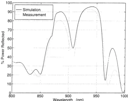
3.9 Simulation of experimental data 2. 2S
5.0 Simulcitecl and measured reflectivities of R C D i. 54
5.6 Simulated and measured reflectivities of RCD2. 54
5.7 Measured reflectivity of etched RCD2 sample. 55
5.8 Simulated reflectivity of etched RCD2 sample... 55
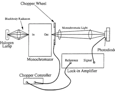
5.9 Photocurrent measurement setup... 56
5.10 Measured photocurrent from the RCD l sample... 58
5.11 Simulation of quantum efficiency for the R C D l sample. 58 5.12 Measured photocurrent from the RCD2 sample... 59
5.13 Simulation of quantum efficiency for the RCD2 sample. 59 5.14 Measured photocurrent from the 300A etched RCD2 sample. 60 5.15 Simulation of quantum efficiency for the 300A etched RCD2 sample. 60 5.16 High speed measurement setup... 61
5.17 High speed measurements at A = 850 n m ... 63
5.18 High speed measurements above GaAs band edge... 64
LIST OF TABLES
4.1 i' inal value of each design parameter... 47
Chapter 1
INTRODUCTION
There has been a fast progress in optical communication, processing and mea surement systems in the last decades in parallel to the development of high bandwidth sources, detectors and transmission media. The optical fiber has proven to be an ideal transmission medium with transmission capabilities that are theoretically four orders of magnitude higher than microwave communica tion systems [1]. To exploit the maximum of this potential, light sources and detectors with very high bandwidths are necessary. Semiconductor sources and detectors, with their fast electrical response and appropriate optical prop erties. have become the dominant devices. Diode lasers were the first semi conductor devices to einplo}^ a Fabry-Perot rnicrocavity to enhance emission properties. Recently, a photodetector structure with similar enhancement of detection properties at resonant wavelengths has been developed [2].
The desired properties for photodetectors in contemporary optical telecom munication technologies are high efficiency along with short response times. The efficiency of a photodetector is stated in terms of its c[uantum efficiency, i.e. the ratio of detected photons to incident photons. Since the absorption takes place as the optical field propagates along the absorbing layer, the quan tum efficiency of a conventional photodetector increases by increasing the ab sorbing layer thickness. The speed of ultrafast detectors, on the other hand, is generally limited by the time that is required for the pliotogenerated carriers
to traverse the absorbing la\^er. Hence, the speed of the device increases by decreasing the absorbing layer thickness. This trade-off between speed and effi ciency leads to the evaluation of the performance of a photodiode in terms of the gain-bcindwidth product. By phicing an absorbing layer inside a Fabry-Perot microcavity, the ciucintum efficiency of a photodetector can be enhanced at the resoricint wavelengths without effecting the speed of the device [2]. The resonant cavity enhcuiced (RCE) detection scheme has been used in different device structures such as Schottky [-3], [4] and metal semiconductor metal (MSM ) [5] photodiodes and heterojunction phototransistors (H PT) [6].
The photodetector structures preferred for high speed applications are Schottky and p-i-n photodiodes [7]. Schottky photodiode consists of a semiconductor-metal junction offering high frequency performcince for a va riety of material combinations. The speed and efficiency of a photodetector is determined by the optical and electronic properties of the materials used. Direct bandgap semiconductors are efficient photon absorbers. For high speed cipplications, direct bandgap materials that have high carrier mobilities are preferred. GaAs, satisfying both the direct bandgap and high carrier mobility requirements, is widely used in high speed applications. GaAs Schottky photo diodes with a 3dB bandwidth exceeding 230 GHz have been demonstrated[8]. The bandgap of the semiconductor also determines the operation wavelength of the photodetector. A semiconductor can not absorb photons with energies less than the bandgap energy. The bandgap energy of GaAs is 1.42 eV, hence GaAs is .sensitive to wavelengths shorter than 880 nm [7]. For longer wa,ve- length high speed applications, InGaAs, whose bandgap energy ma.y be as low as 0.36 eV [7] depending on the In concentration, is the preferred semiconduc tor.
In this thesis, we present our work on the characterization and design of G aA s/A lA s RCE Schottky photodiodes with a thin InGaAs absorbing layer. The optical field can be coupled to the microcavity either through the semi transparent Schottky metal (top illumination), or through the GaAs substrate (l)ottom illumination). Devices for both cases are designed by maximizing the absorption of the optical field in the InGaAs absorbing layer. The analysis of the optical held distribution within the resonant cavity is done by using a scattering matrix (S-matrix) method [9,10]. The loss in the Schottky metal and
the field distril:>ution in the cavity are calculated exactly and the dependence of quantum efhciency on various device parameters is investigated.
In Chapter 2, the operation principles of Schottky photodiodes are reviewed and the basic limitations on the speed and efficiency of the devices are ex plained. The S-matrix method used to analyze optical properties is outlined in Chapter 3. In Chapter 4, the steps followed to design the photodiodes are explained. In Chapter 5, the measurements on various fabricated diodes are presented and compared with simulations. (Jonclusions and discussions are presented in Chapter 6.
Chapter 2
Schottky Photodiodes
High-speed photodetectors are very important components in realizing the maximum potential of high-bandwidth optical systems. Photodetectors with shorter response times improve the information transmission capacity of opti cal communication systems by increasing the overall system bandwidth. Faster photodetectors also provide higher temporal resolution in the measurement of short optical pulses. Another important measure in evaluating the performance of a photodetector is its responsivity (current per optical power). For a pho todetector to be useful, it has to have a high responsivity at the wavelength band of interest.
Photons absorbed by a semiconductor generate mobile charge carriers (an electron-hole pair per absorbed photon). Semiconductor based photodetec tors are designed either as photoconductive devices or photodiodes. Photo- conductive devices operate by sensing the increase in the conductivity of the material, which is a result of the photogenerated charge carriers. Photodi odes. on the other hand, operate by transporting the photogenerated carriers rapidly through the diode junction, by means of the strong electric field that is supported in the junction depletion layer (the space-charge region at the junction, where the carrier densities are depressed). Photodiodes are classified in terms of the junction types forming the diode (p-n, p-i-n, Schottky [7]). .A p-n photodiode is a p-n junction whose reverse current increases when carriers
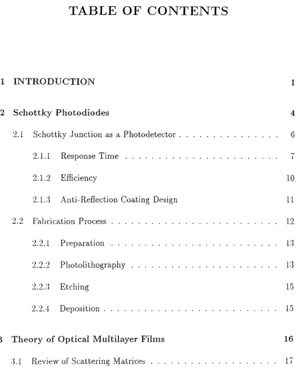
are Photogeaerated. A p-i-n photodiode is a p-n junction, with tin intrinsic (i) layer between the p and layers. The absorption of photons close to, l)ut outside of the depletion layer causes a slow diffusion of photogenerated carriers into the depletion layer. This effect decreases the speed of the device. One of the junction layers may be replaced with a metallic layer to increase the speed of the device, by minimizing the diffusion effect. The resulting device is called a Schottky photodiode and is shown in Figure 2.1.
In this chcvpter, the operation principles of Schottky photodiodes are re viewed. First, the limitations on the temporal respon.se of Schottky photodi odes are presented. The responsivity aspects of the diodes are later discussed. The design of an anti-reflection coating to increase the responsivity is explained. In the last section of the chapter, the processes necessary to fabricate a Schot tky photodiode are discussed.
E.
' /
V
2.1
Schottky Junction as a Photodetector
Schottky photodiodes are formed from metal-serniconductor junctions. When the metal and the semiconductor blocks are joined, charges transfer through the junction until thermal equilibrium is reached. In thermal equilibrium, the Fermi levels of the two materials become equal. The energy-band diagram of a junction formed by a metallic layer on an n-type semiconductor is shown in Figure 2.1, where, the energy level of the bottom of the semiconductor conduc tion iDand is denoted by Ec·, and the top of the semiconductor valence bcind is denoted l.)y E^. The difference between these two levels is tlu^ semiconductor bandgap energy E., = Ec — Ey. The common Fermi level of the materials is denoted li\· E j. The energy difference between the vacuum level and Ec is the electron affinity, denoted by y. The energy difference between the vacuum level and the Fermi level is the metal work function, denoted by IT. The injection of electrons from the metal into the semiconductor conduction band is prevented by the potential barrier IT —y. This barrier causes a depletion region of width cl with a total voltage drop of Vq across this region to be formed. The device
shown in Figure 2.1 is called a Schottky barrier diode and acts as a voltage rectifier just like a p-n junction.
The Schottky diode shown in Figure 2.1 can be used as a photodetector when reverse biased. Figure 2.2 shows the device of Figure 2.1 in this mode of operation. In the figure, d is the depletion Uwer, where the mobile carrier densities are degraded as a result of charge transfer at the junction. The velocities of electrons and holes are denoted respectively by rv; and u/i- The N~ layer is an n.-type semiconductor, which may be totally depleted when the diode is reverse biased. The layer is also an ?r-type semiconductor, with a higher doping concentration. Typical doping concentrations are N~ ~ 10^' cm “ ^ and
,Y+
^ 10^·'^ cm~^. The layer serves to contact the cathode of the .Schottky diode {N ~ layer) to the e.xternal circuit. This type of contact is called an ohmic (bilaterally resistive) contact, which prevents the formation of another Schottky junction at the cathode of the device. Applying negative bias (negati\'e voltage at the metal end) widens the depletion width d and in this way, all the N~ region can be depleted. The reverse bias also enhances the electric field E in the depletion region. When photons with photon energy hu greater lhan the-e — X — ---
d-x
bariclgap energy of the material are absorbed in the semiconductor, electron- hole pairs are generated. The portion of these carriers, that are generated in the depletion region, are swept away by the electric field inducing a photocurrent ip in the external circuit.
2.1.1
Response Time
When a photon is absorbed at an arbitrary position x in the depletion region, it creates an electron-hole pair as shown in Figure 2.2. The hole moves towards the Schottky metal (towards the left in the figure) with a velocity Vh and the electron moves away from the metal with velocity Ue· A carrier of charge Q that moves with velocity v{t) in the semiconductor induces an external current given by [7]
Q
i{t} =
(
2.
1)
(Q, v) being ( —e, We) fo>·' electrons and (e, y/J for holes, respectively. The essence of Equation 2.1 is that as long as a carrier is moving in the semicon ductor {v{t) 0), it contributes to the current in the external circuit. Since the carriers generated at position x have to travel the distances x and d — x in the semiconductor, and this requires time intervals th = xjvh and t. = (d — .r)/iy,
the current measured in the external circuit is not instantaneous. The to tal charge induced in the external circuit due to the absorption of a single photon can be found by integrating the hole and electron currents given by Ec(uation 2.1 to line!
vii X Vp d — X
r/ = e— — +
e-d Vh d = e. (2.2)
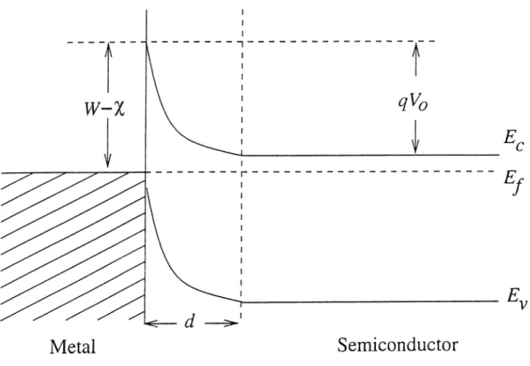
as expected. The response time of the device to a single photon is thus limited by the transit times and th of the carriers, the ultimate limit being the carrier that arrives later at the device terminals depending on the position X (an electron arrives at the Schottky metal, whereas a hole arrives at the j'Y+-yY- interface). The optical excitation usually has more than one photon and this results in photogeneration of carriers throughout the depletion region rather than at a single position x. The simplest case occurs assuming unifoi'm photogeneration along the depletion region. Figure 2.3 shows the hole, electron and total current due to a uniformly photogenerated total charge of Q [7]. Since the velocity of the holes is lower than the velocity of electrons, the latest arriving carrier is a hole generated at the N'^-N~ interface traversing the whole depletion region. The response time is equal to d/u/i.
From the above discussion, it is clear that the response time of the device increases with increasing depletion layer width. This is an important limitation, called the transit-time limit, which plays an important role in determining the speed of semiconductor devices, including Schottky photodiodes. When the detector material has a high absorption coefficient, most of the carriers are generated close to the Schottky metal. A similar situation occurs wdaen absorption occurs only in a thin absorbing layer, that is placed close to the
Qvj^/d
Figure 2.3: Photocurrent pulse shape for uniform absorption along the deple tion laver.
Schottky metal. The structure of the resonant cavity enhanced photocletectors (to be discussed later in Chapter 4) is such that, the absorption occurs in a thin absorbing layer, which is placed inside a thicker depletion region. The absorbing layer is placed close to the Schottky metal and the distance to the A'·*· layer is much longer. Hence, it is safe to assume that absorption occurs close to the metal surface. Under these conditions, the holes have to travel a shorter distance and the electrons are the limiting carriers. When the holes quickly reach the metal, their transport does not contribute to the current, and the electrons arr; the only carriers remaining to induce current. .All the electrons rea.ch the A" *· layer approximately at the same time, therefore we Ccui expect a rectangular current pulse [llj as given by
w =
/0 0 < t < te 0 L < t
(2.3)
where Iq is the magnitude of the induced current. In frequency domain, r i \ ·
Ip[uj) = smc The 3-dB roll-off frequency is given by
(2.4)
ft3—dB = 0.442 1 - (2.5)
The induced photocurrent is measured on a load resistor (as shown in Figure 2.4). The capacitor Cj. is the diode depletion layer capacitance and is given by
a (2.6)
where c and A are the permittivity of the material and the area of the diode, respectively. The RC circuit shown in Figure 2.4 also limits the transient response of the diode, where the 3-dB roll-off frequency is given by
d r'3—dB
__
J
rc
—
'IttRi sA (2.7)It is seen from Equations 2.5 and 2.7 that there is a trade-off between the effects of the two poles. The transit-time limited bandwidth is inversely proportional to the depletion layer width d whereas the RC time-constant limited bandwidth is directly proportional to it. To overcome this limitation, the area of the diode
can be decreased. However, diodes with areas smaller than 10/an'- are not leasible, because focusing of the optical beam becomes difficult and the series resistance ol the diode increases with decreasing area.
Another limitation to the temporal response of the diode is the diffusion of carriers that are generated in undepleted regions into the depletion region. The diffusion time of such carriers also effects the overall response. In a top- illuminated resonant cavity photodiode (to lx; discussed in Chapter 4), typically less than 10% of the light incident on the .Scliottky metal is rrausrnitted into undepleted regions. When the optical beam is well focused onto the diode area, the diffusion effect mгıy be neglected.
2.1.2
Efficiency
Another figure of merit for photodiodes is the quantum efficiency. In general, all photons incident on the photodiode do not create electron-hole pairs. The quantum efficiency ?/ is defined as the probability that a single photon inci dent on the photodiode will induce current in the external circuit. Quantum efficiency depends both on the optical and electronic properties of the semi conductor material and the physical structure of the device. Depending on materials, wavelength, and physical structure, only a portion of the incident optical power is absorbed in the depletion region, whereas the remaining por tion is reflected, transmitted, or absorbed in lossy regions such as the .Schottky
metal. The quantum efficiency is experimentally measured by the ratio of the absorbed optical power contributing to photocurrent to the incident op tical power. Since the number of detected electrons is ecpuil to the number of absorbed photons (neglecting recombination), quantum efficiency may also expressed as [7]
of detected electrons /p /e
7/ = (
2
.8
)# of incident photons Pin/hu
where Pin is the incident optical power, h is Planck’s constant, 2/ is the fre quency of the incident light. Ip is the measured photocurrenr,. and e is the electronic charge. Another expression for quantum efficiency is
V
= (I - R)(l -
(2.9)where R is the surface reflectivity and a is the i^ovver absorption coefficient of the detector material. In the equation, the first term represents the power that penetrates through the front surface of the photodiode. The second term rep resents the portion of the power that is absorbed along a layer of width d. From Equation 2.9, it is observed that, to increase rj either R should be decreased or d should be increased. The front surface reflectivity can be minimized us ing a dielectric coating as will be discussed in the next section, however, as was discussed in previous section, d can not be increased without increasing tlie transit-time. Another readily measurable figure is the responsivity 'R, the ratio of external photocurrent to incident optical power, expressed as
n = P = ^ .
P in h u
(2 .10 )
2.1.3
Anti-Reflection Coating Design
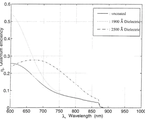
To increase the quantum efficiency of the photodiode, an anti-reflection coat ing rnciy be used on top of the Schottky metcil. The quantum efficiency for the coated photodiode can be calculated using a transmission line analogy em ploying Scattering matrices. This method will be discussed in greater detail in Chapter 3. The calculated quantum efficiency for a GaAs Schottky photodi ode having a depletion region width 0.3 ¡.tm. with Si.-jN.i dielectric coatings of different thicknesses is shown in Figure 2.5. From the figure, it is seen that by
Figure 2.5: Quantum efficiency improvement using dielectric coating. The curves are for uncoated, 1900
A
dielectric coated, and 2500A
dielectric coated diodes.depositing dielectric coatings of different thicknesses, it is possible to shift the wavelength corresponding to peak quantum efficiency.
2.2
Fabrication Process
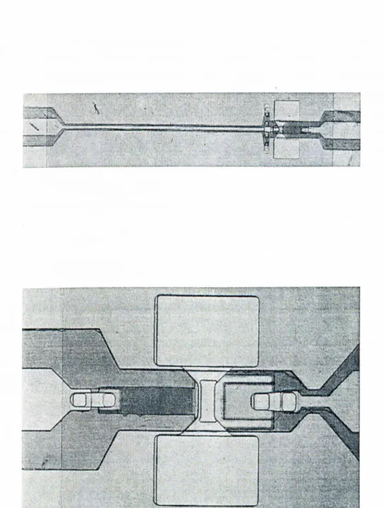
The properties and limitations of photodetectors also depend on the meth ods used to fabricate them. During the fabrication, the desired patterns are transferred onto the semiconductor surface using a mask (a plate with a ge ometrical pattern recorded on it) for each step. This is accomplished by a series of processes. The pattern on the mask is first transferred onto a pho toresist layer (a layer that is sensitive to ultraviolet light e.xposure) covering the semiconductor surface. Then, the patterns on the photoresist are copied onto the semiconductor surface by means of various methods such as etching and deposition. Figure 2.6 shows the photomicrograph ol labricated devices. The diode shown in the first photomicrograph is a device with an absorbing
area of 7 /im x l4 /irn . These devices are designed for transit-time limited high speed measurements. The device shown in the second photomicrograph has a.n area of 120/an xlOO/aa. The devices with larger areas are used for spectral elhciency measurements.
The resonant-cavity wafers that we have designed (to be discussed in Chap ter 4), were grown at Iowa State University and the photodetectors were fab ricated in the Physics Department at Bilkent University. In this section, a l)rief discussion of tlic; fabrication process and the methods that are employed is given.
2.2.1
Preparation
The mask used in the fabrication process is 0.5 c m x 0.5 cm. The wafer was cut to O.ScmxO.Scm samples. Mechanical and/or chemical cleaning methods such as brushing, boiling in chemicals, leaving in flowing de-ionized (DI) water, drying under Nitrogen gas flow and dehydration baking were employed before various process steps.
2.2.2
Photolithography
Photolithography is the proce,ss of patterning an ultraviolet light sensitive pho toresist material to be able to transfer desired geometric shapes onto the sam ple. First, the photoresist is poured onto the wafer and spun at 4000 rpm to achieve a uniform coating. The sample is baked dry and it is turned into a photographic plate. Then, the wafer is exposed to ultraviolet light through the mask plate that contains the desired pattern. Finally, the resist is developed and after an inspection of the success of the process, the samples are taken to the etching process.
Figure 2.6: Photomicrograph of fabricated diodes, (a) Device with an area of 7 /im x Id^ari. (b) Device with an area of 120/.imx 100/mi.
2.2.3
Etching
The patterns defined by photolithography are transferred onto the semicon ductor l)y means of etching. Etching is removal of the regions that are not protected by the photoresist pattern. Wet etching is a method that employs chemicals. The disadvantage of wet etching is that it is isotropic, i.e. it etches in all directions removing some material under the photoresist. Etching steps that are not much sensitive to isotropy such as mesa isolation and ohmic metal deposition were done by wet etching. In contrast, to etch patterns that require strictly vertical etching such as airbridge posts, reactive ion etching (RIE) was used. In this method, die wafer is etched with ion bombardment. Since the ions are accelerated in vertical direction, a vertical etching is achieved.
2.2.4
Deposition
Plasma enhanced chemical vapour deposition (PECVD) is the method that is used to deposite dielectric coatings (Si3N4) on the wafer. This is accom plished in a low pressure, high temperature chamber. The Schottky (Au) and ohmic contact metals as well as interconnect metals are deposited by thermal evaporation.
Chapter 3
Theory of Optical Multilayer
Films
A large variety of multilayer optical films are used in contemporary optical technology. These films find usage either in integrated devices such as verti cal cavity surface emitting lasers (VCSEL), resonant cavity enhanced (RCE) photodetectors, tunable micromachined Fabry-Perot filters [12] or in lumped elements such as dielectric mirrors. Also, the analysis of many optoelectronic components such as p-i-n, Schottky, and metal-semiconductor-metal (M.SM) photodetectors, heterojunction phototransistors (HPT) may be done by con sidering these devices to be composed of layers, and then using the tools to analyze multilayer films. A stack is a multilayer composed of materials that have different refractive indices. In a stack, there cire dielectric interfaces be tween material layers. These interfaces cause a series of multiple reflections of the incident held along the stack. Layers that have loss are modeled with a comple.x refractive index. In the design of an optical multila3fer stack, it is desirable to be able to calculate the reflection and transmission of the optical power at any boundary as well as the absorption in various lossy layers. In the literature, diflerent methods including transmission cind transfer matrices [13], impedance transformation [14], and self consistent consideration of the opti cal held [14] are employed to analyze multilayer stacks. Another systematic
metliod to analyze multilayer structures is the S-matrix (scattering-mcitrix) approach [15]. Whereas the above mentioned methods have limitations in cal- crdating the losses or the exact distribution of the held within the cavity, the S-matrix approach is unique in its power to evaluate the exact held distril^ution in pcissive structures.
3.1
Review of Scattering Matrices
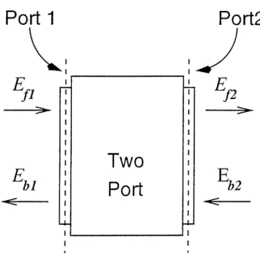
In the S-nicitri.x approach, a transmission line analogy that considers each ma terial layer in the stack as a two port transmission line with a normalized characteristic impedance Z = 1/n is used. Here n is the refractive index of the medium. As it is common in transmission line theory, traveling waves are used to characterize the optical two ports. The S parameters give the waves leaving the two port in terms of the waves entering the two port [9, 10].
In Figure .3.1, E fi denotes the forward traveling wave incident at port 1 and El,2 denotes the backward traveling wave incident at port 2. Ei,i and E j2
are the l)ackward traveling wave leaving port 1 and the forward traveling wave leaving port 2, respectively. Since the wave equation is linear, superposition of the wave equations at the ports yields
Ej2
El, I
¿12 Г21 ri2 ¿21 Ejx Еь2 (3.1)where /,·, and rij are the respectively transmission and reflection coefficients for the electromagnetic wave traveling from port i to port j . The (2 x 2 ) matrix on the right side of Equation 3.1 is known as the scattering-matrix for the two port in Figure 3.1.
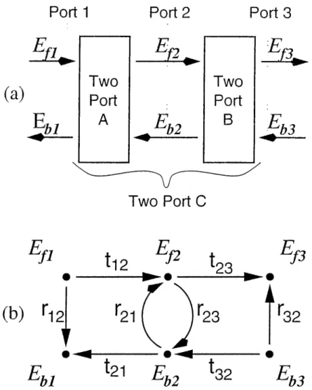
The rules for cascading scattering matrices are derived using Figure 3.2. In Figure 3.2(a), two-ports A and B are cascaded to form the two-port C. The signal flow-graph in Figure 3.2(b) represents the S parameters for the two-ports A and B. the nodes symbolize the traveling waves at input or output ports, where any wave component can be written as the sum of the incoming arrows to the node representing that wave component.
Port 1
Port2
Figure 3.1: Traveling waves entering and leaving a two-port.
Examination of the signal flow-graph in Figure 3.2(b) yields four equations for the traveling waves at the corresponding ports in terms of the input variables E fi and Ehs. These are
Ef2 = t\2Efi-\-r2lEb2 (3.2)
Eb2 = r2sEf2 -f ¿32^63 (3.3)
Eb\ = r\2Efi + t2\Eb2 (3.4)
Ej3 — ¿2 3F//2 + 1'32Eb3· (3.5)
The Equations 3.2 and 3.3 are coupled wave equations and have to be solved simultaneousljc Solving for E f2 and Ei,2 we get,
Ej2 Eb2 t\2Efl -b l'2li32Elj3 1 — /‘23 ■'"21 ¿32 Eb3 + •'"23^12^/1 i — '/’23''’ 21 (3.6) (3.7) 18
(a)
Port 1
Port 2
Ports
^ f 2 ^
Two
Two
Port
Port
A
B
^ b 3Two Port C
(b)
<'12
Figure .'j.’i; (a) Schematic showing the cascaded two-port, (b) Signal how-graph for the cascaded two-port.
Substituting these into Ecpiations 3.4 and 3.5 yields
IP ¿23^12 r , f , ’’'iih-ihi , p Efs — --- E fi -f I r32 -b --- I Eh2 i - r-23r21 1 - r^sr-n JP f , '23^12^21 ^ jp
,
¿2lFi2^
Ehi = ’/’ 12 + ^--- E f i + ----Eb 3. \ 1 — r23'/’21 / 1 ~ /'23/’21 Equations 3.8 and 3.9 are combined in matrix form,Ej3
¿ 1 3 /’ 3 1'Efi
■ . . . ' 3 3 ¿31 .Eb3
_ (3.8) (3.9) (3.10) 19T h e (2x2) m a tr ix o n th e rig h t side of E q u a tio n 3.10 is th e S - m a tr ix lo r th e c a s c a d e d tw o -p o rt in F ig u r e 3.2(a) a n d T.3 — Í. 3 1 — t\2Í23 ’>"31 — 1'32 + ''Зз — ''32 -г 1 - Г23Г21 t21^31 1 — ' ’ 2 3 ' ’ 2 1 ' ’21^23^32 1 — Г2 3Г21 12^21 1 - r23'’21 a re th e e le m e n ts o f th e S - m a tr ix for th e tw o -p o rt C in F ig u re 3.2(a ). (3.11) (3.1 2) (3.13) (3.14)
3.2
S-Matrix Analysis of Optical Multilayer
Films
In th is s e c tio n , c a lc u la tio n o f a b s o rp tio n , re fle c tio n a n d tr a n s m is s io n of lig h t u s in g S -m a tric e s is d e s c rib e d . In th e follow ing a n a ly s is , th e lig h t is a s s u m e d to be c o n s is tin g o f p la n e h a rm o n ic w aves, e x p re s s e d by
E = . (3 .1 5)
U n d e r n o r m a l in c id e n c e c o n d itio n s , th e p ro b le m o f d e te r m in in g th e o p tic a l h e ld d is tr i b u tio n in th e s tr u c t u r e sim p lifie s to d e t e r m in in g th e fo rw a rd a n d b a c k w a rd tr a v e lin g w ave a m p litu d e s in e a c h la y e r. T h e g e o m e tr y o f th e sim p lifie d p r o b le m is sh o w n in F ig u re 3.3.
In th e figu re, th e b o u n d a r ie s lie a t 2: = i = 1 ,2 ,... a n d th e y co v er th e e n t ir e x-y p la n e . T h e fo rw a rd (in c id e n t) E -field p r o p a g a te s in th e + z d ir e c tio n a n d th e b a c k w a rd (re fle c te d ) E -field p ro p a g a te s in th e —2- d ir e c tio n . As is also s e e n fro m F ig u re 3.3, th e sim p lifie d o n e d im e n s io n a l p ro b le m is to find all field p h a s o rs Eji,Ei>i, i = 1,2, .. .
^bl
= Z i
z= Ebi = Z i z= ‘ k+1 ^ i k + 1) ^b(k+l) Z—Zi,F ig u re .3.3: (.l('o rn etry o f th e 1-D p r o b le m in a m u ltila y e r o f iilm,s.
T o b e a b le to r e p r e s e n t o p tic a l la y ers u s in g S -m a tric e s , s im p le b u ild in g b lo c k s a re u se d . T h e S -m a tric e s for th e s e b lo c k s a re th e n c a s c a d e d to o b t a i n th e S -m a tri.x re p re .s e n ta tio n o f la rg e r s ta c k s . T h e s im p le s t case is a la y e r t h a t d o e s n o t c o n ta in a n in te rfa c e . In F ig u re 3 .4 (a ), th is ty p e of a la y e r is s h o w n . T h e m e d iu m h a s a comple.K r e f r a c tiv e inde.x n = ur + ini to a c c o u n t for a b s o r p tio n lo sses. T h e fo rw a rd a n d b a c k w a rd p r o p a g a tin g field p h a so rs u n d e rg o a p h a s e s h ift d u e to th e le n g th d of th e m e d iu m . H o w e v er, sin ce th e r e is n o p h y s ic a l in te r f a c e , no re fle c tio n o c c u rs . In th e c a se o f a c o m p le x r e f r a c tiv e inde.x, th e m a g n itu d e s of th e field p h a s o rs a re also m o d ifie d c o rre s p o n d in g to a lo ssy m e d iu m . T h e fo rw a rd a n d b a c k w a rd p r o p a g a tin g fields c an b e w r itt e n as
(3 .1 6 )
w h e re k = 'ItturIX a n d a = iTrnifX a re c a lle d th e p ro p a g a tio n a n d a tte n iu itio n c o n s ta n ts r e s p e c tiv e ly a n d A is th e fre e -s p a c e w a v e le n g th of th e in c id e n t lig h t. T h e (2 x2) m a tr ix on th e rig h t sid e of E q u a tio n 3.16 is th e S -m a tri.x fo r th e la y e r in F ig u re 3 .4 (a ).
In th e case of a p h y s ic a l in te r f a c e ei,t z = Zq b e tw e e n tw o s e m i-in fin ite m e d ia w ith re fra c tiv e in d ic e s ui a n d as sh o w n in F ig u re 3 .4 (b ), th e r e fle c te d a n d t r a n s m i t t e d fields m a y b e w r itt e n in S -m a tri.x n o ta tio n as
Ej [Z
= d+)
^ikd-fd
0
' Ej{Z = 0 - ) '
_
Ei{Z = 0-)
_
0
gikd-fd
_
Ek(Z
= d+) _
E A Z = Z i ) a , ( z = z „ -) i\2 '^'21 ^’12 ¿21 E ,( Z = Z i ) EAZ = Z i ) 21
n
n
n
"2
z=0
z=d
z=2o
F ig u re 0.4; Bci.sic Iciyers u sed in c a lc u la tin g S m a tric e s : (a) S im p le la y e r, (b ) In te rfa c e . w h e re ¿12 — ¿21 — 7’ 12 — T21 = 2n i ni + 712 2ri2 Ui + 712 721 - 722 721 + 722 722 — 72i (3 .1 8 ) (3 .1 9 ) (3 .2 0 ) (3 .2 1 ) 72l + 722
a r e F re s n e l’s re fle c tio n a n d tr a n s m is s io n c o e fficien ts for n o rm a l in c id e n c e [7], a n d th e (2x2) m a tr ix o n th e r ig h t sid e o f E q u a tio n 3.17 is th e S -n ic itrix for th e in te rfa c e in F ig u re 3.4(b ). U sin g th e tw o S -m a tric e s in E q u a tio n s 3.16 a n d 3.17 a n d th e ru le s for c a s c a d in g S - m a tr ic e s , th e S - m a tr ix r e p r e s e n ta tio n o f a n y p a s s iv e o p tic a l m u ltila y e r s ta c k m a y b e c a lc u h ite d .
T h e o p tic a l p o w er a s s o c ia te d by a p la n e w ave expres.sed as in E c p ia tio n 3.15 is g iv e n by
(3.22)
71
^ = F i r l ^ o 2rjo
w h e re n is th e re fra c tiv e in d e x of th e m e d iu m a n d r/o — 377 fi is th e v a c u u m c h a r a c te r i s t ic im p e d a n c e for e l e c tr o m a g n e tic w aves. T h e o p tic a l r e f le c tiv ity cincl tr a n s m is s iv ity of o p tic a l tw o -p o rts for a n y p o r t a re d e fin e d as th e r a tio o f th e re fle c te d a n d t r a n s m itt e d p o w ers to th e in c id e n t po w er w h e n no p o w e r is in c id e n t fro m th e o th e r p o r t. U sin g E q u a tio n 3.22. th e p o w er r e f le c tiv ity a n d tr a n s m is s iv ity for th e tw o -p o rt in F ig u re 3.5 a re
Port 1
Port 2
.. ^ T P
1 1^2 * 1
F ig u re 3.5: R e fle c iio n a n d tr a n s m is s io n of p o w er fro m a tw o - p o r t.
R - = b’-r·^
J-Iij — 1 / IJ 1 (¿,i) = (l,2),(2,l) (3.23)
To = Tii (tj) = (l,2),(2,l) (3.2.4) w h e re i?,·,· a n d 2}j a r e r e s p e c tiv e ly th e p o w e r re fle c tiv ity a n d tr a n s m is s i v ity for p o w e r in c id e n t o n p o r t f, a n d r'ij a n d i,y a re th e p a r a m e te r s of th e S - m a tr ix for th e tw o -p o rt in F ig u re 3.5.
3.2.1
Calculation of Absorption
In g e n e ra l, th e to ta l a b s o r p tio n in a m u ltila y e r s ta c k is
/!(% ) = 100 - B.{%) - T {% ). (3 .2 5 ) H o w e v er, in m o s t of th e cases, a b s o r p tio n o c c u rs in m o re t h a n o n e la y e r a n d o n e n e e d s to d is c r im in a te b e tw e e n a b s o r p tio n in d iffe re n t la y e rs. T o f o r m u la te th e a b s o r p tio n , th e s ta c k sh o w n in F ig u re 3.6 is irsed.
T o c a lc u la te th e a b s o r p tio n b e tw e e n p o r ts 2 a n d 3, th e s ig n a l flo w -g ra p h in F ig u re 3.7 is u sed . S in ce no p o w e r is in c id e n t o n p o r t 4, Ei,4 = 0, a n d u s in g E q u a tio n s 3.6 a n d 3.7 th e fo rw a rd a n d b a c k w a rd tra v e lin g w av es a t p o r ts 2
Po
(11
Por;t
2
Pprt
3
Pprt
4
P
in
n-
n . absorptive la y e rn-
n.
F ig u re 3.6: A b s o rp tiv e la y e r in a s ta c k . a n d 3 a re fo u n d to b e Ef^ = tg E fi 1 - ruVi i - 2,:3 E l)i — i — 2,.3. T h e p o w e r a b s o rb e d b e tw e e n p o r t 2 a n d p o r t 3 is PA = i P 2 f + P 3 b ) - i P 2 b + P 3 f ) . (3 .2 6 ) (3.2 7 ) (3 .2 8 )w h e re Pij a n d Pu, a re th e p o w ers a s s o c ia te d w ith th e fo rw a rd a n d b a c k w a rd tr a v e lin g w aves a t p o r t i. T h e first te r m in E ciu atio n 3.28 c o r r e s p o n d s to th e
F ig u re 3.7: S ig n a l flo w -g rap h to c a lc u la te a b s o r p tio n .
p o w e r e n te r in g th e a b s o r p tiv e la y e r a n d th e se c o n d te r m gives th e p o w e r le a v in g th e la y er. U sin g E q u a tio n s 3.2 2, 3.26, a n d 3.27 it is fo u n d t h a t
Pa = P .in 1 ---- p l 2 |'" ’- I / I |1 1 — lr-241 'n.3|^ 12 i — |r:34|· --- « 1 3
J-.
---T ■l’24/’2 i r | i - r 2 4 r 2 l | (3 .2 9 ) w h e re Pin is th e p o w e r in c id e n t o n p o r t 1, tij a n d rq· a re th e tr a n s m is s io n a n d re fle c tio n c o e fficien ts for th e e le c tr o m a g n e tic w ave in c id e n t o n p o r t i in th e S -rn a trix b e tw e e n p o r ts i a n d j . T h e h rs t te r m in th e p a r e n th e s is a b o v e c o rre s p o n d s to th e p o w e r tr a n s m i t t e d from p o rt 1 to p o r t 2 a n d th e s e c o n d t e r m c o rre s p o n d s to th e p o w er tr a n s m itt e d fro m p o r t 1 to p o r t 3. T o c a lc u la te th e a b s o r p tio n w h e n th e p o w e r is in c id e n t o n p o r t 4, th e in d ic e s 1 a n d 4 s h o u ld b e in te r c h a n g e d a n d th e in d ic e s 2 a n d 3 s h o u ld b e in te r c h a n g e d in t h e a b o v e e q u a tio n . In cases w h en th e re is po w er in c id e n t o n b o th p o r ts 1 a n d 4, th e p r in c ip le o f s u p e r p o s itio n m a y b e used .3.2.2
Determination of the Field Distribution
S in c e th e r e a re b o th fo rw a rd a n d b a c k w a rd tra v e lin g w aves in a m u ltila y e r s ta c k , th e r e is a s ta n d in g w ave p a t t e r n d u e to th e d e s tr u c tiv e a n d c o n s tr u c t iv e in te r f e r e n c e of th e o p p o s ite p r o p a g a tin g w aves. In s o m e cases it is d e s ir a b le to c a lc u la te th is field d is tr ib u tio n . As it w ill b e se e n in C h a p t e r 4. e x a c t k n o w le d g e of th e field d is tr i b u tio n w ith in a r e s o n a n t c a v ity p h o t o d e t e c t o r is e s s e n tia l. To c a lc u la te th e field d is tr ib u tio n , E q u a tio n s 3.26 a n d 3.27 m a y b e u s e d . T h e E -field a t a n a r b i t r a r y p o s itio n 2 in th e s ta c k c a n b e w r i t t e n as £ (--) = ( l + i - . z ) : t:Oz - E
/0
1 - r,zr,o w h e re th e p o in ts .2 = 0 a n d 2 = Z a re th e tw o e n d s o f th e s ta c k . (3 .3 0 ) 253.3
Simulations on Published Data
In th is s e c tio n , th e S -rn a trix m e th o d d is c u s s e d in th e p re v io u s s e c tio n s is u se d to s im u la te p u b lis h e d e x p e r im e n ta l re s u lts o n re s o n a n t c a v ity - e n h a n c e d s t r u c tu r e s . For c o m p a ris o n p u rp o s e s , th e e x p e r im e n ta l d a t a a re also in c lu d e d .
F hgure 3 .8 (a ) p re s e n ts e x p e r im e n ta l d a t a [4] o n r'esoricmt c a v i ty - e n h a n c e d Id P T s ( h e te r o ju n c tio n p h o to tr a n s is to r s ) w ith a 2 0 0
A
A u c o a tin g o n th e to p . In th e fig u re, th e a u th o r p re s e n ts w a v e le n g th tu n in g of th e p h o t o t r a n s i s t o r s p e c tr a l r e s p o n s iv ity b y m e a n s of c h a n g in g th e le n g th of th e m ic r o c a v ity in th e s tr u c t u r e . T h is is a c c o m p lis h e d by m e a n s o f e tc h in g th e s e m ic o n d u c to r s u rfa c e . T h e d iffe re n t c u rv e s c o rre s p o n d to th e m e a s u re d p h o to c u r r e n t fo r d e v ic e s t h a t h a v e b e e n e tc h e d 1050A,
700A,
a n d 350A.
A c u rv e for a d e v ic e t h a t h a s n o t b e e n e tc h e d a t all is also in c lu d e d . F ig u re 3 .8 (b ) is th e s im u la tio n o f th e s a m e s tr u c t u r e r e p o r te d in [4] u s in g .S -m atrices. T h e p e a k w a v e le n g th s o b ta in e d fro m th e s im u la tio n w ere in g o o d a g re e m e n t w ith e x p e r im e n ta l v a lu e s. .'\ v a r ia tio n b e tw e e n 0.25 a n d 0.35 in th e p e a k c iu a n tu m efficien cy fo r d iffe re n t d e v ic e s is p r e d ic te d b y th e s im u la tio n , w h e re a s th e p eak s for d iffe re n t d e v ic e s d o e s n o t se e m to v a ry in th e e x p e r im e n ta l d a ta . T h is is p r o b a b ly d u e to th e f a c t t h a t th e a u th o r h a s re s c a le d th e p e a k s in F ig u re 3.8(a ). A lso to n o te is t h a t th e im p ro v e m e n t in th e q u a n tu m effic ien cy of th e d e v ic e s is s im u l a te d to b e h ig h e r th a n th e a c tu a lly m e a s u r e d d a ta . T h is is b a s ic a lly d u e to th e id e a ln e s s of th e m o d e l u s e d in th e s im u la tio n s .F ig u re 3 .9 (a ) show s a n e x p e r im e n ta l r e fle c tiv ity m e a s u r e m e n t [16] o f a re s o n a n t c a v ity e n h a n c e d S c h o ttk y p h o to d e te c to r . T h e s tr u c t u r e is a b o t t o m il lu m i n a te d d e v ic e w ith a 1500
A
A1 c o a tin g o n th e to p . S im u la tio n in (b ) p e r f e c tly fits th e e x p e r im e n ta l d a t a in (a) a ro u n d th e re s o n a n c e w av ele n g th . (Ar = 1530 n m ). H o w e v er, th e r e is a d iffe re n c e b e tw e e n th e e x p e r i m e n t a l a n d s im u la te d p lo ts o u ts id e th is re g im e . T h is is d u e to th e fa c t t h a t , a l th o u g h th e w a v e le n g th d e p e n d e n t r e f r a c tiv e in d e x of A lIn A s [17] w as u s e d , th e w a v e le n g th d e p e n d e n c e of th e r e f r a c tiv e in d e x o f th e q u a te r n a r y In G a A lA s w as n o t a v a ila b le a n d a s s u m e d c o n s ta n t th r o u g h o u t th e w a v e le n g th re g im e of in t e r e s t.W A V G1..E N G T H Cnm )
F ig u r e 3.8: S im u la tio n (b ) o f e x p e r im e n ta l d a t a (a ). T h e firs t p lo t c o rre s p o n d s to 1050
A
e tc h e d d e v ic e , th e s e c o n d 700A
e tc h e d d e v ic e , th e th ii d 350.A
e tc h e d d e v ic e , a n d th e f o u rth a s-g ro w n d e v ic e .a ш хи 5>J ГіГг ^
,
İ-Cı L .ı.?j L lü'j / \ i \ / V -X- Ji^1 1CQ U.C3 L-:C'J LXCO îü^u lüCÜ ş*i X i ıiı]“^** S T S
l;C3 ійСО 1500 іѵ-ѵ'О
F ig u re 3.9: S im u la tio n (b) of e x p e r im e n ta l da,ta (a ).
Chapter 4
A lA s/G aA s RCE Schottky
Photodetectors with an InGaAs
Active Region
In o pticcil te le c o m m u n ic a tio n a n d m e a s u r e m e n t s y s te m s , p h o to c le te c to r s w ith h ig h q u a n t u m efficien cies a re d e s ira b le to m in im iz e s y s te m losses. T h e q u a n t u m effic ien cy of th e s e d e v ic e s is lim ite d b y th e th ic k n e s s d o f th e a ljs o rb in g la y e r a n d is g iv e n by E q u a tio n 2 .9, w h e re R is th e su rfa c e re f le c tiv ity a n d a is th e p o w e r a b s o r p tio n co e ffic ie n t of th e a b s o rb in g m a te r ia l. For a - 10"* cm ~^ ( ty p ic a l v alu e for G a A s a n d In G a A s a ro u n d b a n d e d g e ), th e pecik c{u an tu m effic ie n c y o f a 0.3/ivn (a ty p ic a l th ic k n e s s for a h ig h s p e e d S c h o ttk y p h o to d i o d e ) th ic k p h o to d e te c to r is lim ite d to 0.25 a n d to ac h ie v e q u a n t u m effic ien cies g r e a t e r th a n 0.80, p h o to d e te c to r s w ith a b s o rb in g la y ers th ic k e r t h a n 1 . 6 /m i a re n e c e ssa ry . H o w ev er, h ig h effic ien cy d e te c to r s w ith th ic k a b s o r b in g la y e rs h a v e p o o r s p e e d re s p o n s e as a c o n s e q u e n c e o f lo n g e r tr a n s i t tim e s in th e th ic k e r d e p le tio n reg io n as e x p la in e d in C h a p te r 2.
T o incre¿ı.se th e q u a n t u m effic ien cy w ith o u t d e c re a sin g th e b a n d w id t h of th e d e v ic e , a th i n a b s o rb in g la y e r m a y be p la c e d in a F a b r y - P e r o t m ic ro c a v ity .
Ill th is m e th o d , th e o p tic a l field cy cles in th e cav ity , b e in g p a r ti a ll y a b s o rb e d e a c h tim e cro ssin g th e th in a b s o rb in g la y e r, h e n c e a m u ltip le -p a s s d e te c tio n is o b ta in e d . T h e s e d e v ic e s a re c a lle d r e s o n a n t c a v ity e n h a n c e d (R C E ) p h o to d e te c to r s [14]. T h e e.xpression for r/ g iv e n in E q u a tio n 2.9 is n o t v alid tor R C E p h o to d e te c to r s . T h e w a v e le n g th s , for w h ich th e o p tic a l h e ld e x p e rie n c e s e x a c tly a n in te g e r m u ltip le o f 27t p h a s e s h ift in o n e r o u n d - tr ip in th e c a v ity cire c a lle d th e r e s o n a n t w a v e le n g th s . T h e c o n se q u e n c e of th e m u ltip le - p a s s d e te c tio n s c h e m e is in c re a s e d c iu a n tu m elE cie n cy a t th e re s o n a n t w a v e le n g th s .
T h e q u a n tu m ethcienc}^ o f R C E p h o to d e te c to r s w ith lossless m ir r o rs w ere c a lc u la te d by K ish in o e t a l.[2]
V = ;i +
1 — \ / RiR-2e~^’^coii{2kL -f t/’i + ’^h) +
(4 .1 )
w h e re R\ a n d R2 a re th e to p a n d b o tt o m m ir r o r re fle c tiv itie s r e s p e c tiv e ly , k is th e p r o p a g a tio n c o n s ta n t, L is th e c a v ity le n g th a n d t/ji a n d -02 a re th e p h a s e s h ifts in tr o d u c e d b y th e to p a n d b o t t o m m irro rs re s p e c tiv e ly . E c ju a tio n 4.1 giv es rj = 0.66 for R\ = 0.7, i?2 = 0 .9, a = 10‘*cm “ \ d = 0.1/um cit th e reso- iicint w a v e le n g th s. T h e m a x im u m a t t a i n a b l e q u a n tu m efficien cy for th e s a m e d e te c to r w ith o u t th e re s o n a n t c a v ity w o u ld b e 0.09. E c ju a tio n 4.1 fo r q u a n tu m efficien cy n e g le c ts th e s ta n d in g w av e effect w h ic h is to b e c o n s id e re d la te r in th is c h a p te r , a n d a s s u m e s lossless m ir r o rs w h ic h is a b a d a s s u m p tio n for a com m onl}· u.sed A u to p m ir r o r. E c ju a tio n 4.1 is p lo tte d in F ig u re 4.1 for R^ - - 0.7, i?2 = 0.9, ad = 0.1, a n d th e q u a n tu m efficien cy o f a c o n v e n tio n a l p h o to d e te c to r w ith s a m e ad is sh o w n by th e d a s h e d line. In F ig u re 4 .1 , th e c h a r a c te r is tic s o f th e p h o to r e s p o n s e o f a n R C E p h o to d e te c to r is e a s ily id e n - tifle d : in c re a s e d q u a n t u m effic ien cy a t th e re s o n a n t w a v e le n g th s is th e c o n s e q u e n c e of th e c o n s tr u c tiv e in te r f e r e n c e b e tw e e n th e fo rw a rd a n d b a c k w a rd p r o p a g a tin g h e ld s, w h e re a s th e q u a n t u m efficiency a t th e o ff-re s o n a n t w a v e le n g th s d e c re a se s d u e to d e s tr u c tiv e in te rfe re n c e .
F ig u r e 4.1: Q u a n tu m e ffic ien cy o f a n R C E p h o to d io d e (so lid ). T h e d a s h e d lin e sh o w s th e m a x im u m a t t a i n a b l e c iu a n tu m effic ie n c y for a c o n v e n tio n a l p h o to d e t e c to r o f s a m e th ic k n e s s .
4.1
RCE Schottky Photodiode Design
R C E p h o to d io d e m irro rs cire e ith e r fo rm e d by s in g le m a te r ia l in te r f a c e s (m e ta l- s e m ic o n d u c to r , a ir- s e m ic o n d u c to r ) o r by s ta c k in g a l te r n a t in g s e m ic o n d u c to r m a te r ia ls h a v in g d iffe re n t re fra c tiv e in d ic e s . R C E S c h o ttk y p h o to d io d e s a re d e s ig n e d as a m ic ro c a v ity b e tw e e n th e S c h o ttk y m e ta l o n to p a n d a s ta c k of a l t e r n a t i n g s e m ic o n d u c to r m a te r ia ls g ro w n in th e s e m ic o n d u c to r a t th e b o t to m . R C E S c h o ttk y p h o to d io d e s w ith 8 la y e rs o f G a A s /A lG a A s re fle c to r [15] a n d 16 la y ers of A lI n A s /A lG a ln A s re fle c to r [3] ha,ve b e e n e x p e r im e n ta lly d e m o n s tr a te d . T h e d e v ic e s sh o w e d 30% a n d 50% im p ro v e m e n ts in re s p o n s iv - ity , re s p e c tiv e ly . T h e fo rm e r d e v ic e is a to p - illu m in a te d d e sig n w ith a s e m i tr a n s p a r e n t .All to p m ir r o r, h o w e v e r in th e d e s ig n c o n s id e ra tio n s th e .Au la y e r is a s s u m e d to b e fu lly tr a n s p a r e n t. O u r c a lc u la tio n s sh o w e d t h a t th e a b s o r p tio n in th e A u m ir r o r in c re a s e s d r a s tic a lly a t th e r e s o n a n t w a v e le n g th s as w ill be d is c u s s e d la te r , h e n c e th e tr a n s p a r e n c y a p p r o x im a tio n for th e A u m ir r o r is n o t
v alid a t th e r e s o n a n t w a v e le n g th s. T h e l a t t e r d e v ic e is a b o tt o m - il lu m i n a te d d e s ig n w ith a h ig h re fle c tiv ity A n to p m irro r.
In th is c h a p te r , th e d e p e n d e n c e o f th e q u a n t u m efficiencies o f tw o d iffe r e n t d e sig n s tr u c t u r e s sh o w n in F ig u re 4 . 2 o n v a rio u s p h y s ic a l p a r a m e te r s a re in v e s tig a te d . B o th d esig n s a re s im ila r in s t r u c t u r e w ith d iffere n ces in th e th ic k n esses of so m e la y e rs. T h e b a s ic d e sig n is a c a v ity fo rm e d b e tw e e n a A n la y e r, s e rv in g b o th as a S c h o ttk y m e ta l a n d a s e m i- tr a n s p a r e n t to p m ir r o r, a n d a h ig h -re fle c tiv ity m n ltila y e r b o tto m m ir r o r. T h e b o tto m m ir r o r of th e c a v ity is fo rm e d w ith a lte r n a t in g A /4 -A /4 A lA s /G a A s la y e rs. B o th A lA s a n d G a A s a r e tr a n s p a r e n t a t th e d e sig n w a v e le n g th of 900 n rn [18]. O n to p of th e b o tt o m m ir r o r , a n u n d o p e d G a A s b u ffer, a n N"·· G a A s la y e r for o h m ic c o n ta c ts , a n d a n N " G a A s d e p le tio n la y e r follow . In th e N ~ G a A s la y e r, a th in Ino.osGao.9 2As a b s o rb in g la y e r is p la c e d .
T \
N GaAs
absorbing
region
InGaAs
N GaAs
r
+
N GaAs
iu
undoped
GaAs
N\'
W s - ' A oAlAs/GaAs
Bottom
Minor
•
••
Incident
l
i
g
h
t
GaAs
substrate
(a)
(b
)
F ig u re 4.2: R G B S c h o ttk y p h o to d io d e s tr u c t u r e . (a) T o p illu m in a tfid . (b ) B o tto m illu m in a te d .
T h e re h itio n b e tw e e n th e In c o n c e n trc itio n x a n d th e b a n d g a p e d g e E o{x) o f In j;G a i_ j;A s is g iv e n by [19]
E,,{x) = 1.42 - l.o 3 x + 0.45a·-. (4 .2 )
T h e In G a A s u se d in th e p h o to d io d e s t h a t w e d esig n e d luid an In c o n c e n tr a tio n o f 0.08. U sing th is v alu e , th e b a n d g a p w a v e le n g th of In G a A s is fo u n d to b e Xrj = 953 n m w h ich is a b o v e th e d esig n w a v e le n g th of 900 nrn. O n to p of th e N “ G a A s la y e r, th e re is th e A u la y e r s e rv in g b o th as a re fle c to r a n d th e S c h o ttk y m e ta l, a n d firuilly th e to p m o s t la y e r is a S i3N4 d ie le c tric a n ti- r e f le c tio n c o a t ing. In F ig u re 4.2(a ) th e to p illu m in a te d d e sig n is sho w n . T h is d e v ic e h a s a n a n ti-re fle c tio n c o a tin g , a s e m i- tr a n s p a r e n t {1^ = 2 5 0 A , R — 0.77 for th e fin al d e s ig n ) A u to p m ir r o r a n d a h ig h r e fle c tiv ity {R — 0.97 for th e fin al d e s ig n ) b o t t o m m irro r. In c o m p a ris o n , th e b o tto m illu m in a te d d ev ice in F ig u r e 4 .2 (b ) h a s a (R — 0.77 for th e final d esig n ) b o tto m m irro r a n d a h ig h r e f le c tiv ity {tm = 1 0 0 0 A , R = 0.94 for th e final d esig n ) A u to p m irro r. A lth o u g h th e e x p re s s io n fo r q u a n t u m efficiency in E q u a tio n 4.1 is h e lp fu l in u n d e r s ta n d i n g th e g e n e ra l c h a r a c te r is tic s of R C E p h o to d e te c to r s , in th e case o f lo ssy m e ta l m ir r o rs a n d a lo ssy c a v ity , th is e x p re s s io n is n o t e x a c t. To o b ta in e x a c t r e s u lts , th r o u g h o u t th is c h a p te r , th e n u m e ric a l m e th o d e m p lo y in g S -m citrice s d e s c r ib e d in C h a p t e r 3 is u s e d to c a lc u la te th e re fle c tiv ity , tr a n s m is s iv ity , loss a n d q u a n tu m effic ien cy s p e c tr a of th e d e v ic e s in F ig u re 4.2.
4.1.1
Bottom Mirror Design
T h e s tr u c t u r e in F ig u re 4.3 is a q u a r te r w av e s ta c k (Q W S ) w h ich c o n s is ts o f a l te r n a t in g A /4 -A /4 h ig h in d e x {nff) - low in d e x (?r£,) la y ers on a s u b s t r a t e m a te r ia l. .Since th e la y ers a re c[u arter w a v e le n g th th ic k , a t th e c e n tr a l fr e q u e n c y a ll re fle c te d b e a m s e m e rg in g fro m p o r t 1 a re in p h a s e , h e n c e th e r e f le c tiv ity o f th e s tr u c t u r e is in c re a s e d w ith in c re a s e d n u m b e r of lay ers. T h e a n a ly s is of s u c h a s tr u c t u r e c a n be d o n e by th e S -m a tric e s m e th o d d e s c rib e d in C h a p t e r 3. T h e S -m a tric e s fo r th e tw o -p o rts b e tw e e n so m e s e le c te d p o in ts in F ig u r e 4.3 a re