Nanoscale Dielectric Capacitors Composed of Graphene and Boron
Nitride Layers: A First-Principles Study of High Capacitance at
Nanoscale
V. Ongun Özçelik
†,‡and S. Ciraci*
,†,‡,§†UNAM-National Nanotechnology Research Center, ‡Institute of Materials Science and Nanotechnology, and§Department of
Physics, Bilkent University, Ankara 06800, Turkey
ABSTRACT: We investigate a nanoscale dielectric capacitor model consisting of two-dimensional, hexagonal h-BN layers placed between two commensurate and metallic graphene layers using self-consistentfield density functional theory. The separation of equal amounts of electric charge of different sign in different graphene layers is achieved by applying an electric field perpendicular to the layers. The stored charge, energy, and the electric potential difference generated between the metallic layers are calculated from thefirst principles for the relaxed structures. Predicted high-capacitance values exhibit
the characteristics of supercapacitors. The capacitive behavior of the present nanoscale model is compared with that of the classical Helmholtz model, which reveals crucial quantum size effects at small separations, which in turn recede as the separation between metallic planes increases.
■
INTRODUCTIONConventional (electrostatic) and electrochemical (EC and/or electrochemical double layer, EDLC) capacitors, batteries, and fuel cells are systems which are widely used for energy storage.1,2 As far as the combination of specific power versus specific energy capability is concerned, electrostatic capacitors keep an important place among them. On the other side, conventional capacitors are limited by the device geometry, and batteries are limited by the slow response time due to the motion of the ions in electrochemical reactions.
Recent developments in nanoscale physics have further widened our perception of energy storage mechanisms in materials. In this respect, recyclable, efficient, and high-capacity energy storage through lightweight nanoscale mediums has attracted interest.3,4In fact, capacitors at nanoscale have been developed as one of the most promising energy storage mediums, whereby higher energy densities several orders of magnitude larger than other storage media have been realized. They are able to store and release charge faster, can deliver higher amounts of charge at higher power rates as compared to conventional batteries, and have longer life with short load cycles which make them advantageous in various applica-tions.1,2,5−9 Several materials, such as mixed metal oxides,10 polymers,11 and carbon nanotubes,12,13 have been used to fabricate supercapacitors. Concomitantly, the performances of the latter were further improved and stabilized by using nonaqueous solvents with a uniform translational diffusion coefficient.14 This important behavior was also observed in simulations of acetonitrile confined in carbon nanotubes, which makes it a suitable solvent.15
Recently, nanoscale dielectric capacitors (NDC) have rapidly developed and achieved properties that are superior to other systems of energy storage. An ideal NDC should be composed of metallic layers that can store and release charge and a dielectric material between these layers for increasing the capacitance value without increasing the dimensions of the structure. Recent theoretical and experimental studies on graphene, carbon nanotubes, and metallic nanowires have focused on understanding the dielectric properties of these structures and forming thin layers that can serve as ideal charge-holding metallic plates.9,16−18 A theoretical method has been developed for calculating the dielectric response of periodic metal-insulator heterostructures and hence the microscopic properties of thin-film capacitors modeled by Ag/MgO/Ag films.9
In a recent study, nanostructured electrodes were used to fabricate transparent capacitors with polymer dielectrics and carbon nanotube electrodes,16which are important in a range of applications from sensors to transparent circuits. Similarly, structural, optical, and electrical properties of transparent carbon nanotube-based capacitors on glass substrates were also examined and shown to be highly efficient in photovoltaic and solar energy storage devices.17 It was also experimentally demonstrated that Ag nanowires deposited on glass substrates can be used as electrodes,18 which can possibly be used in nanocapacitor fabrication.
Improving the permittivity of the dielectrics that are used has also been important for higher capacitance values of NDCs. Received: April 15, 2013
Revised: June 30, 2013
Published: July 1, 2013
reason behind the reduction in the capacitance values in experiments as compared to theoretical predictions was explained.9
Exceptional properties of graphene have been exploited actively for future nanoscale electronics and spintronic applications.22,23 Incidentally, it was shown that graphene can sustain current densities 6 orders of magnitude larger than copper.24 Graphene, with its 2D one-atom-thick honeycomb structure showing a perfect electron−hole symmetry and high chemical stability,25 has also been proposed as an ideal nanocapacitor material.5,26,27 In previous studies, capacitance per unit area values of 80 and 394μF/cm2have been achieved for capacitors with electrodes comprising pristine graphene and multilayer reduced graphene oxide.28 Other than obtaining high-capacitance values, graphene capacitors have also been a field of study for observing interaction phenomena in graphene layers.29
■
MODELIn this paper, we consider an NDC model envisaged from composite materials and study its capacitive behavior using ab initio calculations within the density functional theory (DFT). Our nanoscale capacitor model is composed of hexagonal h-BN layers, which are stacked between two metallic graphene sheets, as described in Figure 1a, and attains high gravimetric capacitance values. We compare the capacitance values obtained from the present first-principles total energy calculations with those estimated within the classical Helmholtz model and reveal crucial quantum size effects at nanoscale.
Single- and multilayer h-BN are wide band gap insulators, and they can serve as dielectric materials between metallic graphene layers. Additionally, sheets of h-BN multilayers that are lattice-matched to graphene allow one to attain robust and high-precision nanoscale spacings between two parallel metallic graphene sheets, which can be set to desired values. It has already been shown both experimentally30and theoretically31,32 that h-BN layers of any thickness can be grown on graphene layers, and vice versa. Additionally, using phonon dispersion calculations and molecular dynamics simulations, the stabilities of such structures and other similar carbon and BN allotropes, namely, graphyne and BNyne, were recently studied.33,34Other than bilayer structures, it is also possible to grow perpendicular carbon and BN chains on top of graphene and single-layer h-BN.35,36
Controlling the spacing between metallic plates at nanoscale is the crucial feature in attaining high capacitances. Series, parallel, mixed, and 3D combinations of these structures, which can also be fabricated by repeated stacking of varying numbers of graphene and h-BN layers, offer a number of options in constructing novel NDCs with diverse functions. Thus, by varying the separation distance in our capacitor model, we observe interesting quantum size effects at small separations,
which recede as the distance between the graphene plates increases. Because the principle objective of using a capacitor is to store energy by storing an equal magnitude of opposite-sign electric charges in two disconnected conducting plates, a charged capacitor is in a static and nonequilibrium state. The energy stored this way is released when the plates are connected to a circuit, so that the discharged capacitor turns into an equilibrium state. At nanoscale, because the separation thickness of the devices can be as small as a nanometer, the stored energy has to be calculated using first principles. However, the availablefirst-principles methods allow us to treat the distribution of only one kind of excess charge (positive or negative) in the same system at a time.37−40 Therefore, the main obstacle in the present study was separating positive and negative charges on the plates of a capacitor. In our model, the charge carriers are electrons themselves; while they exist in excess in one plate, they are depleted from the other one. Thus, our paper treats the charged capacitor. The charge separation is achieved by applying an external electricfield E⃗, perpendicular
Figure 1.(a) NDC model with n = 2 h-BN layers serving as dielectrics is capped by two parallel graphene layers serving as metallic plates. The whole system is subjected to a uniform electricfield along the z-axis so that graphene plates are charged by surface charge densities of −σ and +σ, respectively. (b) Schematic description of the calculated (x,y)-plane averaged electronic potential, V̅(z). The difference of the potential energy between graphene layers A and B is eV̅z. (c)
Isosurfaces of the self-consistent difference charge densities of the negatively charged (A) and positively charged (B) graphene layers are ΔρA and ΔρB, respectively. The isosurface values are taken as 0.01
electrons/Å2. Yellow and blue isosurfaces indicate excess and depleted electrons, respectively. The computations are performed on a 2× 2 supercell with a vacuum spacing of 20 Å.
to the graphene layers, as is schematically shown in Figure 1a. This situation mimics the operation of a capacitor, whereby the surface charge of opposite sign initially stored on different metallic plates creates a perpendicular electric field. The shorting of these two plates and, hence, the discharge of the capacitor are hindered by not placing a sufficient amount of vacuum space or dielectric h-BN layers between graphene plates.
On the other side, charge separation through the applied electric field by itself brings along a serious problem: When treated using periodic boundary conditions (PBC), the vacuum potentials between the periodically repeating negatively charged surfaces or systems under an electricfield form a quantum well. If this quantum well dips below the Fermi level, electrons start to be accommodated in this quantum well in calculations using a plane-wave (PW) basis set. Accordingly, excess electrons in the graphene layers become vulnerable to spurious charge spilling into the vacuum space between supercells. Therefore, this artifact sets a limit to the amount of negative charging that can be treated by PW for a given width of the vacuum region s. Nevertheless, this artifact of PW methods can be circumvented by using a local basis set such as atomic orbitals (AO) because they fail to represent the states which can be bound to the quantum well in the middle of the vacuum spacing. In recent studies,41,42 the treatment of charged systems and systems under electricfield has been extensively analyzed. Thus, treating an NDC from the first principles using periodic boundary conditions, where electric charges of opposite sign are separated through an applied perpendicular electric field, is the unique aspect of our study.
■
METHODSIn view of the above discussions, we carried outfirst-principles spin-polarized and spin-unpolarized calculations within density functional theory (DFT) using atomic orbitals (AO) as the local basis set. The exchange-correlation potential is approxi-mated by the generalized gradient approximation (GGA) using the Perdew, Burke, and Ernzerhof (PBE) functional.43 The eigenstates of the Kohn−Sham Hamiltonian are expressed as
linear combinations of numerical atomic orbitals. A 200 Ryd mesh cutoff is chosen, and the self-consistent field (SCF) calculations are performed with a mixing rate of 0.1. Core electrons are replaced by norm-conserving, nonlocal Troullier− Martins pseudopotentials.44The convergence criterion for the density matrix is taken as 10−4. Atomic positions and lattice constants are optimized using the conjugate gradient method, where the total energy and atomic forces are minimized. In particular, the minimum energy stacking sequence of the composite material, consisting of n BN layers between two graphenes, is determined for each n. All numerical calculations are performed using the SIESTA code.45Dipole corrections46 are applied in order to remove spurious dipole interactions between periodic images for the neutral calculations. Calculations are carried out on the (2 × 2) supercells in order to account for possible reconstructions, but the relevant values are given per primitive cell. The dielectric constant values of stacked boron nitride layers were calculated using plane-wave methods as implemented in the PWSCF package.47 Our previous analysis48has shown that the interlayer spacing of graphite has been overestimated by GGA approximation using PW91 functional,49but it has improved to near 4% of the experimental value with the van der Waals (vdW) correction.50 To reveal the accuracy of the spacing between graphene and single-layer h-BN and also the spacing between the graphene layers capping two h-BN layers (Figure 1a), we optimize the structures with two different methods: (i) with PBE using SIESTA code and (ii) with PBE including vdW correction using VASP code.51While the spacing between single graphene and h-BN layers is overestimated by 5.5% in PBE relative to that obtained by including the vdW correction, this over-estimation of the spacing between the graphene layers in our capacitor model is reduced to 1.5%. As for the lattice constant of the hexagonal primitive unit cell predicted by PBE (SIESTA) and PBE+vdW (VASP), the former method overestimates the lattice constant of the free graphene (free h-BN) by only 0.6% (0.7%). Because h-BN layers serve as dielectrics, the over-estimation of the interlayer spacings by approximately 5.5% is acceptable.
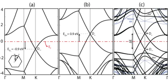
Figure 2.Electronic energy band structures calculated for the (2× 2) supercell. The zero of energy is set to the Fermi level EF, shown by the red
dash-dotted lines. (a) Isolated, single-layer graphene, which is negatively charged by Q =−0.06e per primitive unit cell (or σ = −0.18C/m2). (b) Positively charged single-layer graphene with Q = +0.06e per primitive unit cell (orσ = +0.18C/m2). E
D±≃ ±0.9 eV are the downward and upward
shifts of the Dirac points (D−and D+) relative to the Fermi level for negative and positive charging, respectively. (c) Electronic band structure of the
capacitor consisting of two h-BN layers capped by single-layer graphenes, which is subjected to an electricfield of E⃗ = 1.0 V/Å. The band structure of the free h-BN bilayer is shown by the blue-dotted lines. The energy difference between D−and D+points isΔE. The inset shows the symmetry
in-plane stiffness, is compressed to the smaller unit cell.
■
RESULTS AND DISCUSSIONElectronic Structures. We first consider two isolated graphene layers where each one is charged by ±Q = 0.06 electrons per primitive unit cell (or ±σ = |0.18C/m2). The electronic band structure of each graphene is shown in Figure 2a,b: The Dirac point D−dips below the Fermi level when the isolated graphene is negatively charged byσ = −0.18C/m2. In contrast, the Dirac point D+ is elevated above the Fermi level when the isolated graphene layer is positively charged or hole doped byσ = 0.18C/m2. The upward and downward shifts of the corresponding band structures in Figure 2a,b are equal and| ED−| = ED+≃ 0.9 eV.
Next, we examine our model of nanocapacitor described in Figure 1a, which is actually one single system of a composite material consisting of two insulating h-BN layers placed between two parallel semimetallic graphene layers. Initially, the graphene layers have zero net charge. However, when exerted by a positive E⃗ along the z-axis, self-consistent field calculations accommodate excess electrons on the left graphene while the same amount of electrons are depleted from the right graphene. Hence, the integral of the volume charge in the cell of the capacitor is still zero; ∫cellQdV = 0. The atomic structures, interlayer spacings, relative positions of the layers, and the cell parameters are optimized. The plane-averaged electronic potential, V̅(z), is shown in Figure 1b, under an external electricfield of E⃗ = 1.0 V/Å. For this case, the potential energy difference between the two graphene layers is calculated to be eΔV̅z≃ 1.8 eV, which leads to the accumulation of equal amount of surface charge of opposite sign,± Q = 0.06 electrons per primitive unit cell (or±σ = 0.18C/m2) on either graphene layers. The isosurface plots of the difference charge density of the negatively charged (A) and positively charged (B) graphene layers, namely the difference of charge densities between the charged (ρA,B) and neutral (ρ0) graphene layers,ΔρA,B=ρA,B− ρ0illustrate the charge separation.
The equilibrium band structure of this optimized capacitor in a (kx,ky,kz = 0) symmetry plane, including the center of the Brillouin zone parallel to the graphene and BN planes of the capacitor, is presented in Figure 2c. Owing to the weak coupling between graphene layers and BN layers, the band structure of the capacitor is practically the combination of the bands in Figure 2a,b and those of h-BN bilayer, as shown by the dotted lines in Figure 2c, except that the insulating bands of each h-BN layer shift relative to each other. Based on the calculated electronic structure, we make the following com-ments:
(i) Being an insulator and serving as a spacer and dielectric, the variation of the band structure and band gap of BN with applied electric field E⃗ is closely related to the breakdown
bent. For a given uniform E⃗ exerted perpendicular to the plates, the band bending is approximately proportional with the width of the dielectric spacer and the magnitude of the electricfield. Upon bending of the bands in direct space, the band gap between the conduction and the valence band decreases with increasing potential difference. In the k-space, the band bending manifests itself as the energy shift of the bands of each parallel h-BN layer. For example, the energy shifts of consecutive bands are calculated to be∼1 eV at E⃗ = 1 V/Å for five layers of BN without the capping graphene layers. Even if the band gap in each layer is practically unaltered, the band gap of the multilayered h-BN decreases with increasing E⃗ because the bottom of the conduction band is lowered along one direction, while the top of the valence band raises along the opposite direction to narrow the band gap. At the breakdown voltage of the BN spacer comprising afinite number of h-BN, the Fermi level overlaps the band of capping graphene (or the top of the valence band of the bare BN spacer in the absence of capping graphenes) with the lowest conduction band, which is bent to lower energies. Thereafter, a resonant tunneling sets in between negatively and positively charged metal plates through the h-BN layers. This physical event has been identified as the Zener breakdown,57 whereby a wide band gap insulator becomes a conductor. The tunneling current exponentially decays with the increasing height and width of the tunneling barrier. In this respect, the nanoscale dielectric capacitor proposed here, having small spacings between the plates, allows a high surface charge densityσ on the metallic plates and, hence, induces large perpendicular electric field in the spacer. The energy barrier, ΔΦ, between the Fermi level and the lowest conduction band of BN spacer is the tunneling barrier. Higher ΔΦ, by itself, hinders the tunneling of carriers from one plate to other through the BN spacer
(iii) At nanoscale, the dielectric strength can be deduced from the band structure of the BN spacer, which is stronger than the dielectric strength of the BN crystal. For the nanoscale graphene + BN, planar capacitor, like the one presented in Figure 1, the breakdown voltage is estimated from the band gap of a single-layer h-BN, which is ∼3 V for n = 3. We note, however, that for the BN spacer consisting of a few layers, the breakdown voltage depends on various conditions, such as the nonequilibrium state and the coupling between graphene and adjacent h-BN, among others, and requires a thorough analysis. (iv) The integrals of the SCF charge on the graphene layers A and B in Figure 2c are equal to the excess charge values used in the calculation of Figure 2a,b, namely∫B,Aσ(x,y)dxdy= ±Q = 0.06 electrons per primitive cell (or ±σ = 0.18 C/m2). The calculated energies of the Dirac points for the left graphene layer, ED−in Figure 2a, and the right graphene layer, ED+ in Figure 2b, relative to the common Fermi level EF, are equal in magnitude because of the electron−hole symmetry near the Dirac points (i.e.,|ED−| = ED+). In the electronic band structure
of the capacitor in Figure 2c, the energy difference between the Dirac points D+and D−isΔE. Interestingly, ΔE is equal to the sum of the energy shifts in Figure 2a,b (i.e.,ΔE = |ED−| + ED+. Even more interesting is thatΔE ≃ eΔV̅zin Figure 1b.
(v) The effect of h-BN spacer layers on the electronic properties of graphene is minute. Hence, the small lattice mismatch between graphene and h-BN layers is not important for the purpose of the present study.
These features, by themselves, demonstrate that our model of NDC is appropriate and precise. Even if the adjacent layers are coupled, the graphene layers A and B are isolated and electronically decoupled. It should be noted that the capacitive behavior attained above by applying a perpendicular electric field is equivalent to the reversed situation, where the ±Q charge stored in different plates can induce the same E⃗.
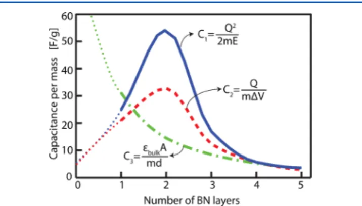
Capacitance. Having tested our NDC model of capacitor, we next investigated its capacitive behavior. To this end, we calculate the stored energy as a function of the applied electric field for different n of parallel h-BN. The energy difference between the total energies of the structures under externalfield and under zerofield gives us the energy stored in the capacitor, EC(n,E⃗ ) = ET(n,E⃗)− ET(n,E⃗ = 0). The total energies, ET, are obtained by SCF energy calculations of the optimized structures. In Figure 3a, the variations of capacitor energy with applied E⃗ are plotted for n = 1−4. The variation of ECis not monotonic with n for the reason explained in the forthcoming part. In Figure 3b, we present the variation of the magnitude of the excess charge, |Q|, stored in either graphene layers as a function of the appliedfield for n = 1−4. Here, |Q| is also obtained from first-principles calculations by
integrating the net charge in either graphene layer. In Figure 3c, we calculate the capacitance per mass C1from the expression C1 = Q2/(2mEC), where m is the total mass of B, N, and C atoms in the model. We note that for E⃗ > 0.35 V/Å, the calculated values of capacitance C1begin to saturate to different values depending on n and become independent of the applied field as one expects. Thus, our choice of E⃗ = 1 V/Å in Figure 2 was reasonable because it is within the saturated region for n = 2. This very important result shows that even if the energy of NDC is obtained from the first-principles calculations, the behavior of the calculated capacitance complies with its definition. The transient behavior of E⃗ in the range of 0 < E⃗ < 0.45 is due to the uncertainty in the calculation of optimized ET. The gravimetric capacitance of n = 2 is calculated to be C1= 54.4 F/gr, which is considered to be in the range of (EDLC) supercapacitors. The capacitance values can also be acquired from the definition, namely, C2= Q/mΔV̅zusing the calculated charge values|Q| in Figure 3b and ΔV̅zfrom the plane-averaged potential V̅(z), as described in Figure 1. The capacitance values acquired this way are in the range of those calculated from C1= Q2/(2mE
T) in Figure 3c. Nonetheless, in the rest of discussions, we used the capacitance values C1obtained from the quantum mechanical calculations of energy and charge because the plane-averaging process of electronic potentialΔV̅zdoes not provide the necessary precision compatible with that of the total energy calculations. In Table 1, we list various parameters and calculated values relevant for the calculations of gravimetric capacitances per unit mass. We do not consider the graphene bilayer corresponding to n = 0 because the charge stored in the layers are shorted.
Figure 3.Variations of stored energy EC, charge|Q|, and capacitance C as a function of external electric field E⃗ calculated for different n number of
h-BN layers between two graphenes. Note that the capacitance values start to saturate after E⃗ > 0.35 V/Å and reach their steady state values for E⃗ > 0.6 V/Å. Table 1a n d m κ |Q| EC V̅z C1 C2 C3 1 6.21 1.21 1.59 0.035 0.033 2.2 24.5 20.9 33.9 2 9.52 1.63 2.17 0.060 0.033 1.8 54.4 32.8 16.5 3 12.23 2.04 2.75 0.055 0.051 3.5 23.2 12.3 10.2 4 15.14 2.46 3.29 0.040 0.093 4.6 5.6 5.7 6.9
aNumber of BN layers between the graphene plates, n; calculated and optimized values of the distance between graphene layers capping h-BN layers,
d (in Å); total mass of the primitive unit cell, m (in kg× 10−22); calculated dielectric constants of the layered h-BN sheets,κ; magnitude of the excess charge on the graphene plates,|Q| (in electrons); energy stored in the primitive unit cell, EC(in eV); local potential difference between the graphene
plates,ΔV̅z(in V); gravimetric capacitance in Farads per grams calculated using (i) the ECand Q values obtained from DFT calculations (i.e., C1=
Q2/2mE; (ii) theΔV̅zand Q values obtained from DFT calculations (i.e., C2= Q/mΔV̅zand (iii) using the classical Helmoltz expression, that is, C3=
κε0((A)/(md)) whereκ is the dielectric constant value for bulk BN, ε0= 8.85× 10⁻¹²F/m is the permittivity of free space, and A = 5.25× 10⁻²⁰m2
is the area of the graphene plate in the primitive unit cell. The relevant values are given for the maximum capacitance values obtained for each n. The masses of the NDC models are calculated by adding the atomic masses of B, C, and N atoms in the primitive unit cell of the optimized composite systems.
capacitance value acquired from the DFT results is small for the single h-BN layer, but it passes through a maximum and then decreases with increasing numbers of h-BN layers. The latter behavior for large number of h-BN layers is reminiscent of that of classical capacitance, namely C∝ 1/d, because the distance d between the charged capacitor plates also increases as n increases. However, the increase in the value of C1 as n increases from 1 to 2 is surprising because the effect of the insulating medium consisting of h-BN layers is indigenous to the DFT calculation of C1deduced from EC. This situation is attributed to a quantum size effect as revealed from our analysis of the high-frequency dielectric constant, κν=∞, as well as the low frequency (static) dielectric constant,κν=0, of h-BN sheets calculated as a function of n. Because of the layered character, one distinguishes the in-plane (∥) and perpendicular (⊥) dielectric constants in the BN spacer. The calculatedκv=0,∥and κν=0,⊥ of the layered bulk BN crystal are 5.25 and 3.80, respectively, which are in fair agreement with experimental values.58Calculated values ofκv=0,∥(κν=0,⊥) are listed in Table 1 for n = 1−4. Accordingly, κ increases with increasing n and displays a strong size effect. Rather small values of κ exist for n = 1 and 2 because C1first increases with increasing h-BN layer for n≤ 2, but it decreases with increasing n for n > 2, as shown in Figure 4. In other words, although a decrease in the capacitance value is expected as the layer−layer separation increases, the increase in the dielectric constant of h-BN layers counters this effect. Hence, as a result of the competition between the increased layer−layer distance and increasing dielectric constant values, the capacitance value passes from a maximum at an optimum spacing after which it starts to decrease again. In the samefigure, we also plotted the variation of capacitance obtained from the Helmholtz model C3=κε0A/ md, where d is the distance between graphene layers corresponding to a given n andκ is the dielectric constant of bulk BN. This is a purely classical value. We see that quantum effects dominate the capacitance for n < 4, while they decay quickly, and the capacitor behaves as a classical capacitor for n ≥ 4.
our model can attain high-capacitance values. This is crucial for high-capacity energy storage. Even in the classical region, for n ≥ 4, the capacitance values of C3are still very high due to the separation of graphene layers at nanoscale. (iii) The DFT method used to separate charges of different polarities between two metallic plates and to calculate the optimized total energy is original and allows us to treat the nanoscale dielectric capacitor from the first principles. (iv) The analysis on the spurious vacuum charging is crucial for the calculations from thefirst principles using periodic boundary conditions, as it is in the present study. These spurious effects have been eliminated by using local basis sets. (v) We also showed that quantum effects become crucial at nanoscale and how they recede as the dimensions of the capacitor increase. Thus, the present model of NDC has promise for future applications. Our model of nanocapacitor allows the sequential and multiple combination of graphene/BN/graphene/BN/.../graphene to achieve high-volumetric densities and to attain high-capacity energy storage. Apart from the graphene/h-BN/graphene composite nano-capacitor, layered composite materials composed of graphene-like insulators GaAs, AlAs, and InN,53among others, which are capped by single-layer metallic Si and Ge (i.e., silicene and Germanene),59 or layered transition metal dichalcogenides56 can be used for the same purposes. Finally, we point out another interesting situation, where the metallic plates and the dielectric medium between them can be arranged on the same single-layer honeycomb structure consisting of graphene and h-BN domains. This way, a 2D capacitor can be realized and integrated to the nanocircuit on the same layer. The recent studies achieving the growth of graphene and h-BN continuously on the same layer60indicate that this conjecture can be promising in the near future. We hope that the present study will initiate further experimental and theoretical studies in thisfield.
■
AUTHOR INFORMATIONCorresponding Author
*E-mail: [email protected].
Notes
The authors declare no competingfinancial interest.
■
ACKNOWLEDGMENTSThe authors thank Can Ataca for his assistance in the calculation of the dielectric constants of h-BN layers. The computational resources have been provided by TUBITAK ULAKBIM, High Performance and Grid Computing Center (TR-Grid e-Infrastructure) and UYBHM at Istanbul Technical University through Grant No. 2-024-2007. This work was supported by TUBITAK and the Academy of Sciences of Turkey(TUBA).
Figure 4.Comparison of the calculated capacitance values of NDC at E⃗ = 1.0 V/ Å as a function of the number of insulating h-BN layers, n. Capacitance values calculated using the optimized total energy ET[n,E⃗]
obtained from DFT, C1, using the plane-averagedΔV̅z, C2, and the
purely classical Helmholtz formula, C3, are shown by solid (blue),
dashed (red), and dash-dotted (green) lines, respectively. The dotted lines show the hypothetical capacitance values for n < 1.
■
REFERENCES(1) Winter, M.; Brodd, R. J. What Are Batteries, Fuel Cells, and Supercapacitors? Chem. Rev. 2004, 104, 4245−4270.
(2) Pandolfo, A. G.; Hollenkamp, A. F. Carbon Properties and Their Role in Supercapacitors. J. Power Sources 2006, 157, 11−27.
(3) Yildirim, T.; Ciraci, S. Titanium-Decorated Carbon Nanotubes as a Potential High-Capacity Hydrogen Storage Medium. Phys. Rev. Lett. 2005, 94, 175501.
(4) Durgun, E.; Ciraci, S.; Zhou, W.; Yildirim, T. Transition-Metal-Ethylene Complexes as High-Capacity Hydrogen-Storage Media. Phys. Rev. Lett. 2006, 97, 226102.
(5) Stoller, M. D.; Park, S.; Zhu, Y.; An, J.; Ruoff, R. S. Graphene-Based Ultracapacitors. Nano Lett. 2008, 8, 3498−3502.
(6) Burke, A. Ultracapacitors: Why, How and Where Is the Technology? J. Power Sources 2000, 91, 37−50.
(7) Holme, T. P.; Prinz, F. B.; Stockum, P. B. High Energy Storage Capacitor by Embedding Tunneling Nano-Structures. U. S. Pat. Appl. Publ. 2010, 91, 1−16.
(8) Zeng, H.; Sun, H.; Luo, W.; Huang, W.; Wang, Z. Nanoscale Capacitance Spectroscopy Characterization of AlGaN/GaN Hetero-structure by Current-Sensing Atomic Force Microscopy. J. Appl. Phys. 2009, 105, 094319.
(9) Stengel, M.; Spaldin, N. A. Origin of the Dielectric Dead Layer in Nanoscale Capacitors. Nature 2006, 443, 679−682.
(10) Toupin, M.; Brousse, T.; Bélanger, D. Charge Storage Mechanisms of MnO2 Electrode Used in Aqueous Electrochemical
Capacitor. Chem. Mater. 2004, 16, 3184−3190.
(11) Rudge, A.; Davey, J.; Raistrick, I.; Gottesfeld, S.; Ferraris, J. P. Conducting Polymers as Active Materials in Electrochemical Capacitors. J. Power Sources 1994, 47, 89−107.
(12) Liu, C. G.; Liu, M.; Li, F.; Cheng, H. M. Frequency Response Characteristics of Single-Walled Carbon Nanotubes as Supercapacitor Electrode Material. Appl. Phys. Lett. 2008, 92, 143108.
(13) Niu, C. M.; Sichel, E.; Hoch, R.; Moy, D.; Tennent, H. High Power Electrochemical Capacitors Based on Carbon Nanotube Electrodes. Appl. Phys. Lett. 1997, 70, 1480.
(14) Futaba, D. N.; Hata1, K.; Yamada, T.; Hiraoka, T.; Hayamizu, Y.; Kakudate, Y.; Tanaike, O.; Hatori, H.; Yumura, M.; Iijima, S. Shape-Engineerable and Highly Densely Packed Single-Walled Carbon Nanotubes and Their Application as Super-Capacitor Electrodes. Nat. Mater. 2006, 5, 987−994.
(15) Kalugin, O. N.; Chaban, V. V.; Loskutov, V. V.; Prezhdo, O. V. Uniform Diffusion of Acetonitrile Inside Carbon Nanotubes Favors Supercapacitor Performance. Nano Lett. 2008, 8, 2126−2130.
(16) Sorel, S.; Khan, U.; Coleman, J. N. Flexible, Transparent Dielectric Capacitors with Nanostructured Electrodes. Appl. Phys. Lett. 2012, 101, 101106.
(17) Uprety, K. K.; Ocola, L. E.; Auciello, O. Growth and Characterization of Transparent Pb(Zi,Ti)O3 Capacitor on Glass
Substrate. J. Appl. Phys. 2007, 102, 084107.
(18) Lee, J. Y.; Connor, S. T.; Cui, Y.; Peumans, P. Solution-Processed Metal Nanowire Mesh Transparent Electrodes. Nano Lett. 2008, 8, 689−692.
(19) Tang, H.; Sodano, H. A. Ultra High Energy Density Nanocomposite Capacitors with Fast Discharge Using Ba0.2Sr0.8Ti3
Nanowires. Nano Lett. 2013, 13, 1373−1379.
(20) Kim, P.; Doss, N. M.; Tillotson, J. P.; Hotchkiss, P. J.; Pan, M. J.; Marder, S. R.; Li, J.; Calame, J. P.; Perry, J. W. High Energy Density Nanocomposites Based on Surface Modified BaTiO3 and a
Ferro-electric Polymer. ACS Nano 2009, 3, 2581−2592.
(21) Tang, H.; Lin, Y.; Andrews, C.; Sodano, H. A. Nanocomposites with Increased Energy Density through High Aspect Ratio PZT Nanowires. Nanotechnology 2011, 22, 015702.
(22) Novoselov, K. S.; Geim, K.; Morozov, S. V.; Jiang, D.; Zhang, Y.; Dubonos, S. V.; Grigorieva, I. V.; Firsov, A. A. Electric Field Effect in Atomically Thin Carbon Films. Science 2004, 306, 666−669.
(23) Netto, C.; Guinea, F.; Peres, N. M.; Novoselov, K. S.; Geim, A. K. The Electronic Properties of Graphene. Rev. Mod. Phys. 2009, 81, 109−162.
(24) Geim, A. K. Graphene: Status and Prospects. Science 2009, 324, 1530−1534.
(25) Geim, A. K.; Novoselov, K. S. The Rise of Graphene. Nat. Mater. 2007, 6, 183−191.
(26) Yongchao, S.; Samulski, E. T. Exfoliated Graphene Separated by Platinum Nanoparticles. Chem. Mater. 2008, 20, 6792−6797.
(27) Vivekchand, S. R. C.; Rout, C. S.; Subrahmanyam, K. S.; Govindaraj, A.; Rao, C. N. Graphene-Based Electrochemical Super-capacitors. J. Chem. Sci. 2008, 120, 9−13.
(28) Yoo, J. J.; Balakrishnan, K.; Huang, J.; Meunier, V.; Sumpter, B. G.; Srivastava, A.; Conway, M.; Reddy, A. L. M.; Yu, J.; Vajtai, R.; Ajayan, P. M. Ultrathin Planar Graphene Supercapacitors. Nano Lett. 2011, 11, 1423−1427.
(29) Yu, G. L.; Jalil, R.; Belle, B.; Mayorov, A. S.; Blake, P.; Schedin, F.; Morozov, S. V.; Ponomarenko, L. A.; Chiappini, F.; Wiedmann, S.; Zeitler, U.; Katsnelson, M. I.; Geim., A. K.; Novoselov, K. S.; Elias, D. C. Interaction Phenomena in Graphene Seen Through Quantum Capacitance. Proc. Natl. Acad. Sci. U.S.A. 2013, 110, 3282−3286.
(30) Liu, Z.; Song, L.; Zhao, S.; Huang, J.; Ma, L.; Zhang, J.; Lou, J.; Ajayan, P. M. Direct Growth of Graphene/Hexagonal Boron Nitride Stacked Layers. Nano Lett. 2011, 11, 2032−2037.
(31) Özçelik, V. O.; Cahangirov, S.; Ciraci, S. Epitaxial Growth Mechanisms of Graphene and Effects of Substrates. Phys. Rev. B 2012, 85, 235456.
(32) Sachs, B.; Wehling, T. O.; Katsnelson, M. I.; Lichtenstein, A. I. Adhesion and Electronic Structure of Graphene on Hexagonal Boron Nitride. Phys. Rev. B 2011, 84, 195414.
(33) Topsakal, M.; Aktürk, E.; Ciraci, S. First-Principles Study of Two and One Dimensional Honeycomb Structures of Boron Nitride. Phys. Rev. B 2009, 79, 115442.
(34) Özçelik, V. O.; Ciraci, S. Size Dependence in the Stabilities and Electronic Properties ofα-Graphyne and Its Boron Nitride Analogue. J. Phys. Chem. C 2013, 117, 2175−2182.
(35) Ataca, C.; Ciraci, S. Perpendicular Growth of Carbon Chains on Graphene from First-Principles. Phys. Rev. B 2011, 83, 235417.
(36) Özçelik, V. O.; Ciraci, S. Self-Assembly Mechanisms of Short Atomic Chains on Single-Layer Graphene and Boron Nitride. Phys. Rev. B 2012, 86, 155421.
(37) Chan, K. T.; Lee, H.; Cohen, M. L. Gated Adatoms on Graphene Studied with First-Principles Calculations. Phys. Rev. B 2011, 83, 035405.
(38) Chan, K. T.; Lee, H.; Cohen, M. L. Possibility of Transforming the Electronic Structure of One Species of Graphene Adatoms into That of Another by Application of Gate Voltage: First-Principles Calculations. Phys. Rev. B 2011, 84, 165419.
(39) Suarez, A. M.; Radovic, L. R.; Bar-Ziv, E.; Sofo, J. O. Gate-Voltage Control of Oxygen Diffusion on Graphene. Phys. Rev. Lett. 2011, 106, 146802.
(40) Topsakal, M.; Ciraci, S. Effects of Static Charging on Exfoliation of Layered Crystals. Phys. Rev. B 2012, 85, 045121.
(41) Gurel, H. H.; Özçelik, V. O.; Ciraci, S. Effects of Charging and Perpendicular Electric Field on the Properties of Silicene and Germanene. J. Phys.: Condens. Matter 2013, DOI: arXiv:1306.5891.
(42) Topsakal, M.; Gurel, H. H.; Ciraci, S. Effects of Charging and Electric Field on Graphene. J. Phys. Chem. C 2013, 117, 5943−5952. (43) Perdew, J. P.; Burke, K.; Ernzerhof, M. Generalized Gradient Approximation Made Simple. Phys. Rev. Lett. 1996, 77, 3865−3868.
(44) Troullier, N.; Martins, J. L. Efficient Pseudopotentials for Plane-Wave Calculations. Phys. Rev. B 1991, 43, 1993−2006.
(45) Soler, J. M.; Artacho, E.; Gale, J. D.; Garcia, A.; Junquera, J.; Ordejon, P.; Sanchez-Portal, D. The SIESTA Method for Ab Initio Order-N Materials Simulation. J. Phys.: Condens. Matter 2002, 14, 2745−2779.
(46) Markov, G.; Payne, M. C. Periodic Boundary Conditions in Ab Initio Calculations. Phys. Rev. B 1995, 51, 4014−4022.
(47) Giannozzi, P.; et al. Quantum ESPRESSO: A Modular and Open-Source Software Project for Quantum Simulations of Materials. J. Phys.: Condens. Matter 2009, 21, 395502.
(52) Wallbank, J. R.; Patel, A. A.; Mucha-Kruczynski, M.; Geim, A. K.; Fal’ko, V. I. Generic Miniband Structure of Graphene on a Hexagonal Substrate. Phys. Rev. B 2013, 87, 245408.
(53) Sahin, H.; Cahangirov, S.; Topsakal, M.; Bekaroglu, E.; Akturk, E.; Senger, R.; Ciraci, S. Monolayer Honeycomb Structures of Group-IV Elements and III-V Binary Compounds: First-Principles Calcu-lations. Phys. Rev. B 2009, 80, 155453.
(54) Watanabe, K.; Taniguchi, T.; Kando, H. Direct Bandgap Properties and Evidence for Ultraviolet Lasing of Hexagonal Boron Nitride Single Crystal. Nat. Mater. 2004, 3, 404−409.
(55) Ataca, C.; Sahin, H.; Akturk, E.; Ciraci, S. Mechanical and Electronic Properties of MoS2Nanoribbons and Their Defects. J. Phys.
Chem. C 2011, 115, 3934−3941.
(56) Ataca, C.; Sahin, H.; Ciraci, S. Stable, Single-Layer MX2 Transition-Metal Oxides and Dichalcogenides in a Honeycomb-like Structure. J. Phys. Chem. C 2012, 116, 8983−8999.
(57) Zener, C. Theory of Electric Breakdown of Solid Dielectrics. Proc. R. Soc. London 1934, 145, 523−529.
(58) Geick, R.; Perry, C. H.; Ruppercht, G. Normal Modes in Hexagonal Boron Nitride. Phys. Rev. 1966, 146, 543−547.
(59) Cahangirov, S.; Topsakal, M.; Akturk, E.; Sahin, H.; Ciraci, S. Two- and One-Dimensional Honeycomb Structures of Silicon and Germanium. Phys. Rev. Lett. 2009, 102, 236804.
(60) Sutter, P.; Cortes, R.; Lahiri, J.; Sutter, E. Interface Formation in Monolayer Graphene Boron Nitride Heterostructures. Nano Lett. 2012, 12, 4869−4874.