∥Department of Chemistry, Bilkent University, 06800 Bilkent, Ankara, Turkey
*
S Supporting InformationABSTRACT: Doping of organic semiconductors enhances the performance of optoelectronic devices. Although p-type doping is well studied and successfully deployed in optoelectronic devices, air stable n-type doping was still elusive. We succeeded with n-n-type doping of organic semiconductors using molecular dopant N-DMBI under ambient conditions. Strikingly, n-type doping accounts for a gigantic increase of the photoconductivity of doped thin films. Electrical and optical properties of the n-doped molecular semiconductor were investigated by temperature dependent conductivity, electron para-magnetic resonance (EPR), and flash-photolysis time-resolved micro-wave conductivity (FP-TRMC) measurements. A significant reduction and saturation in activation energy with increasing doping level clearly suggests the formation of an impurity band and enhancement in carrier density. Computational studies reveal the formation of a charge transfer
complex mediated by hydrogen abstraction as the rate-determining step for the doping mechanism. The colossal enhancement of photoconductivity induced by n-doping is a significant step toward optoelectronic devices made of molecular semiconductors.
KEYWORDS: molecular doping, organic semiconductor, photoconductivity, N-DMBI, Fermi level
1. INTRODUCTION
Molecular doping of organic semiconductors with electron acceptors (p-doping) or electron donors (n-doping) increases conductivities and enhances the performance of optoelectronic devices by lowering energy barriers for charge injection and reducing ohmic losses.1,2 Employment of doped multilayer structures has been successful in advancing the device efficiencies in organic photovoltaics,3−8
perovskite solar cells,9 and organic light emitting diodes (OLEDs).10−17 Especially, p-type doping is extensively studied for a wide range of different dopant/organic semiconductor combina-tions.18−21In contrast, efficient n-type doping is more difficult to achieve, and a lack of stable n-type systems has so far limited the realization of p-i-n multilayer structures. To achieve n-type doping, semiconductor and dopant are required to fulfill the following conditions: (i) both the n-dopant and n-type semiconductor have to be stable in ambient atmosphere; and (ii) the electron affinity of semiconducting material should match or exceed the ionization potential of the dopant.22−24
The first ever case of n-type molecular doping of organic semiconductors was achieved with tetrabutylammonium salts.25 Recently, derivatives of reduced 1,3-dimethyl-2-phenyl-2,3-dihydro-1H-benzo[d]imidazoles (DMBI) such as
N-DMBI and DMBI dimers,26−29 e.g., (2-Cyc-DMBI)2, have
emerged as promising donors. Alternatively, radical ions produced by cleaving of organometallic complex dimers30 such as Cr2(hpp)4and (RuCp*(mes)2)2can transfer electrons.
Nevertheless, there have been few reports on synthesis and n-doping of small air stable molecular hosts at room temperature. Jen et al.31 reported n-doping of quinoidal thienoisoindigo nitrile (DCN) by ammonium and phoshonium salts in solution at room temperature, leading to conductivities around 10−2S cm−1. Bao et al.32 synthesized several n-dopant precursors based on benzimidazole derivatives for doping of fullerene in solution.
The practical utility of molecular doped organic semi-conductors motivated extensive efforts to understand the fundamental doping mechanism,33−36 as microscopic under-standing of the underlying physics and doping mechanism is still lacking. Recently, Ortmann and co-workers have used simulations and experimental techniques to resolve the Fermi
Special Issue: Young Investigator Forum
Received: November 6, 2019
Accepted: December 22, 2019
energies and density of states for fullerene doped with benzimidazoline radicals (2-Cyc-DMBI).35The induced intra-gap states and other parameters affecting the conductivity and charge-carrier generation infilms were analyzed systematically, further correlating the doping efficiency and electronic properties of organic semiconductors. Despite these studies, the chemical instability at ambient conditions represents a major challenge to extend the scope of doped organic semiconductors in optoelectronic devices.
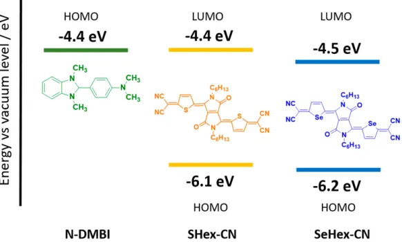
In this paper, we investigate the physical and electrical properties of organic semiconductors, doped with n-dopant (N-DMBI) at ambient conditions. The molecular structures of dopant and host pairs and corresponding energy levels36,37are shown inFigure 1.
We systematically probed the formation of polarons in n-doped solutions by UV−vis and near-IR (NIR) spectroscopic measurements accompanied by electron spin resonance (ESR) spectroscopy in drop-cast doped films. We then correlated electrical properties of doped thin films with varying dopant concentrations by performing bulk conductivity measurements
using two- and four-probe methods. The electrical conductivity is strongly dependent on the dopant concentration up to a threshold above which doping has no significant effect on the electrical conductivity.
Further evidence of n-doping is provided byflash-photolysis time-resolved microwave conductivity (FP-TRMC) measure-ments, which found a stupendous enhancement of photo-conductivity. We have rationalized this phenomenon with the reduction in activation energy for doped films. These results shed light on the importance of the energy levels of the n-type dopant and host to obtain an air stable n-type doped thinfilm of an organic semiconductor.
2. RESULTS AND DISCUSSION
To reveal the degree of chemical doping between dopants and host matrices (SHex-CN and SeHex-CN), absorption spectra were analyzed systematically by varying the amount of dopant (Figure S1). All the measurements were carried out in the solution state at ambient conditions. As shown in Figure 2a, the neutral sample of SHex-CN exhibits clear dual band Figure 1.Chemical structures and energy levels of host molecules SHex-CN and SeHex-CN (estimated from redox potentials) and n-dopant N-DMBI.
and 784 nm (strong). The weak low-energy absorption is mostly due to the HOMO−SOMO (singly occupied molecular orbital) transition, and the strong peak is due to the SOMO− LUMO transition.
These absorptions are typical for radical anions (and cations). Simultaneously with the appearance of radical anion absorptions, the dopant mixing results in a reduced intensity of absorbance of the neutral sample. Since N-DMBI dopant absorbs exclusively in the UV region below 350 nm, the in situ spectra indicate effective charge transfer from N-DMBI to SHex-CN in solution and n-type chemical doping of SHex-CN. The doping process was accompanied by a distinct color change. The color changed slowly from blue to pale green and finally to pale blue. A similar trend was observed in the case of
SeHex-CN doping with N-DMBI (Figure 2b). During the
course of addition of N-DMBI solution to pure SeHex-CN in chlorobenzene, a strong polaronic peak gradually intensified at 885 nm, which was accompanied by bleaching of the absorption peaks of the neutral species at 600 and 640 nm.
UV−vis−NIR spectra were also analyzed in thin films to confirm the chemical doping of SHex-CN (Figure S2). The pristine SHex-CNfilm shows a broad absorption ranging from 550 to 1050 nm. Introduction of N-DMBI leads to the appearance of a new broadened peak at 990 nm, owing to charge transfer from N-DMBI to SHex-CN in the solid state. The stability of anions and plausible doping mechanisms were investigated theoretically (for details, see methods section in Supporting Information). Theory reproduces the spectral changes upon doping and confirms therefore the formation of anion radicals. The doping reaction between SHex-CN and N-DMBI is initiated with either a hydrogen or hydride transfer , resulting in formation of SHex-CN radical anions as products (Figure S6a). This is in agreement with previous reports on mechanistic investigations of N-DMBI doped fullerene.28,32
The n-type chemical doping of SHex-CN and SeHex-CN was also followed by electron spin resonance (ESR) spectros-copy. ESR spectra were collected of drop-cast pristine and
doped films under ambient conditions. Both pure SHex-CN
and SeHex-CN samples do not exhibit ESR signals. The addition of 5 and 10 wt % dopant leads to the appearance of intense resonant ESR signals at a magnetic field of 3350 G, reflecting the formation of radical anions (Figure 3). The corresponding g-values are 2.004 and 2.003 for SHex-CN and SeHex-CN doped with 10 wt % N-DMBI, respectively. The exclusive evolution of a sharp ESR peak on addition of dopant confirms effective n-doping and electron injection in the solid state, in accordance with UV−vis−NIR absorption spectra.
The combination of ESR and UV−vis−NIR spectroscopy
experiments carried out at ambient atmosphere proves that n-doped SHex-CN and SeHex-CN are air stable.
In order to understand the effect of doping on photo-conductivity and photoinduced charge transfer in bulk films, we have carried out flash-photolysis time-resolved microwave conductivity (FP-TRMC) experiments for neutral and doped samples. This is a fast, reliable, and electrodeless technique to measure intrinsic photoconductivity as φΣμ, where φ is the carrier generation quantum yield upon photoexcitation, and Σμ is the sum of intrinsic charge-carrier mobilities, i.e., the sum of hole and electron mobilities (μhandμe), respectively.
SHex-CN and SeHex-SHex-CN stock solutions were prepared in CHCl3
having a concentration of 6 mg/mL. N-DMBI (dissolved in CHCl3) was added in wt %, and the resulting solutions were
kept for stirring in glovebox overnight. All the films were prepared by drop-casting at room temperature from the corresponding solutions.
Upon photoexcitation with a 355 nm laser, both pristine films of SHex-CN and SeHex-CN showed photoconductivities of 3.8 × 10⁻⁵ and 2.4 × 10⁻⁵ cm2 V−1 s−1, respectively as shown inFigure 4a. A sharp increase in photoconductivity was observed for SHex-CN upon doping with 1 wt % N-DMBI, which further increased with the increase in concentration of dopant to 5 and 10 wt %. A 32-fold enhancement inφΣμ was observed with the maximum value of transient photo-conductivity as 1.2 × 10⁻³ cm2 V−1 s−1 for the 10 wt % doped sample. Such an increase in photoconductivity compared to that of pure Shex-CN arises due to the efficient photoinduced charge transfer from n-dopant to the semi-conductor.
The magnitude ofφΣμ shows a prompt rise after addition of dopant to SHex-CN, but the overall kinetic profiles show similar transient decay rates with minimal change. This indicates that doping induced electron transfer to the semiconductor generates a significant concentration of intrinsic charge carriers, thereby improvingφ followed by higher φΣμ numbers. Similarly, we have assessed the photoconductivity of SeHex-CN, before and after doping with N-DMBI using FP-TRMC measurements. All the films were excited with a 355 nm laser pulse. Compared to pristine SeHex-CN,φΣμ of the 1 wt % N-DMBI doped sample increases by 5 orders of magnitude to 9.6× 10⁻⁵cm2 V−1s−1. On doping to 5 and 10 wt %, a maximum photoconductivity value at 10 wt % of 1.7× 10⁻³ cm2 V−1 s−1is reached, which corresponds to a 70-fold
rise in photoconductivity compared to the pristine sample (Figure 4a). This is one of the highest values of photo-conductivity achieved for the n-type doped organic semi-conductors. For a better analysis, the maximum value of photoconductivity φΣμmax has been plotted for all samples
Figure 3.EPR spectra before and after addition of N-DMBI to SHex-CN and SeHex-SHex-CN.
with varying dopant concentration inFigure 4b, which shows a saturation plateau with 10 wt % dopant.
We have carried out bulk conductivity measurements to evaluate the effect of doping on the charge-carrier density of SHex-CN and SeHex-CN. The doping concentration depend-ence on electrical conductivity is plotted for both of the hosts. The conductivity measurements were performed for drop-cast films by two- and four-probe methods. As shown inFigure 5,
the pristine sample of SHex-CN shows very low conductivity around 10−6 S/cm. Gradual addition of N-DMBI leads to an exponential increase in conductivity with the highest value of
0.01 S/cm achieved for the 10 wt % N-DMBI doped film
(Figure 5). At a low concentration of guest molecules, dopants beginfilling deep-lying traps, improving transport through the film. The influence of trap defects and partial activation of dopants in organic materials is responsible for significant conductivity values even at higher dopant concentrations.
We further increased the dopant concentration from 11 to 15 wt %, but the sample displayed lower conductivity. A drop in conductivity as a result of disrupted morphology is observed when a large fraction of dopant molecules per host are introduced into the crystal lattice. The conductance measure-ments of SeHex-CN samples after doping with N-DMBI show a similar trend. However, the maximum value of electrical
conductivity achieved for doped SeHex-CN films is much
higher, up to 0.1 S/cm at 10 wt % doping. As discussed above in optical and EPR spectroscopic studies, there is clear
evidence of generated polarons or free charge carriers after addition of n-dopant in both the solution and solid state. This suggests that the presence of doping-induced charge carriers are responsible for increasing the conductivity of both materials. A particular trend was followed for all plots of electrical conductivity versus doping concentration in both samples. For SHex-CN, a gradual improvement in conductivity was observed upon increasing the amount of N-DMBI from 1 until 10 wt %, raised by about 104times for 10 wt % dopedfilm
as compared to the pristine sample.
To quantitatively understand the nature of electronic transport in the doped films and the impact of doping, we carried out low-temperature measurements for various doping concentrations. The measurements were performed in a cryostat under high-vacuum conditions (∼10−6 mbar) in a T range between 140 to 305 K. The linearity of the source drain bias (VDS) vs source drain current (IDS) characteristics (IDS−
VDS) across all temperatures and doping concentrations
ensures good ohmic contact between the film and the gold electrodes.Figure 6a,b presents the IDS− VDScharacteristics at
different values of T from samples with doping concentrations of∼10 and 1 wt %, (seeFigure S7for IDS− VDScharacteristics
from the undoped sample). Conductance increases as T increases in all samples across various values of doping, which indicates the semiconducting nature of thefilm. Conductance
(G I V V d d 0 = = ) as a function of T
−1for all samples with various
values of doping concentration, ranging from 0 (undopedfilm) to 10 wt %, is presented inFigure 6c. The arrow indicates the incremental values of doping. The temperature dependence of G was found to follow the Arrhenius relation G = Aexp(−ΔE/ kBT), signifying the activated nature of charge-carrier transport
across the semiconducting channel at all doping concen-trations. Here,ΔE is the thermal activation energy, and kB is
the Boltzmann constant. A is a prefactor, which can be considered to be a constant for a particular doping concentration. ΔE is calculated from the slope of ln G vs 1/ kBT in the higher T regime. ΔE as a function of doping
concentration is presented inFigure 6d.
Charge-carrier transport via thermally activated mechanism is very common for organic semiconductors.38−40 In this mechanism, the electrons (e) from the Fermi level (EF) are
thermally activated above the mobility edge, overcomingΔE = Eμ − EF to contribute to charge transport. Here, the T
dependent variation of Eμis negligible, because the variation of thermal energy (kBT varies from ∼13 to ∼26 meV) in our
Figure 4. (a) Transient photoconductivity of drop-casted films after doping of pristine SHex-CN and SeHex-CN with different doping concentrations of N-DMBI. (b) Plot of maximumφΣμ with dopant concentration.
Figure 5. Electrical conductivity as a function of increased dopant concentration for thinfilms of SHex-CN and SeHex-CN doped with N-DMBI.
experimental T range (from 140 to 305 K) is significantly smaller than theΔE and the width of the Gaussian density of states (DoS) of the conduction band. In solid-state semi-conductors, EFis raised by increasing doping (n-type doping),
and hence, ΔE is reduced. In our case, however, ΔE is
observed to decrease with increasing doping up to 2 wt % and then saturates at∼180 meV as doping is increased to 10 wt %.
This weak doping dependence of ΔE of SHex-CN suggests
that there occurs a sharp peak in the DoS approximately 180
meV below Eμ (equivalent of the conduction band (CB)
minimum), which we identify as the impurity band. This impurity band is possibly created by DMBI dopants and lies ∼1.5 eV above the valence band (VB) maximum of SHex-CN. Although such saturation of ΔE can also be created by the Gaussian DoS of the LUMO band (conduction band) of SHex-CN, the position of the impurity band is consistent with absorption spectra of N-DMBI doped SHex-CN, where a sharp absorption peak is observed at 1.5 eV. Notably, the temperature dependence of G was found to be inconsistent with the variable range hopping scenario, which involves transport in the band tail and can be found in theSupporting Information (Figures S8 and S9). The experimentally observed Fermi level pinning is schematically explained in Figure 6e, presenting a tentative DoS vs E diagram. In this situation, EF
does not change with increasing doping concentration due to
the presence of DB with a sufficiently high DoS, as
experimentally observed inFigure 6d.
Powder X-ray diffraction was used to collect distinctive diffraction patterns of neutral and n-doped samples. Analysis of pristine samples SHex-CN and SeHex-CN showed high crystallinity giving rise to sharp diffraction peaks. Figure S10
shows the powder X-ray patterns as obtained for SHex-CN (blue) and SeHex-CN (red).
The diffractograms of both the molecules consist of multiple peaks within 2θ = 3−30°. The d-spacing of the peak positioned (100) corresponding to a 2θ value 8° in SHex-CN increases to 9.1° for SeHex-CN. The incorporation of the selenium atom in the molecular backbone instead of sulfur leads to an obvious red shift in d-spacing, owing to the bigger atomic size of Se compared to S and greater interelectronic repulsion in case of the Se based system. The d-spacing of 3.7 Å corresponding to 2θ = 23.9° for SHex-CN and 3.2 Å (2θ = 27.4°) agrees well with the intermolecular π−π stacking distance as obtained from the single crystal X-ray diffraction experiments (d = 3.6 Å for SHex-CN and 3.3 Å for SeHex-CN).41−43
Upon doping SHex-CN with N-DMBI, the X-ray diffraction pattern exhibits very low-intensity peaks at same 2θ positions as the pristine sample. This implicates that the ordered structure and orientation between SHex-CN molecules could not be retained after doping, reflecting low crystalline packing in the doped state. However, the lamellar packing and π−π stacking distances remained the same after mixing SHex-CN with N-DMBI as that in pure material. The decrease in the intensity of diffraction peaks after increasing the dopant concentration from 0 to 10 wt % with no resultant peak shifts implies that smaller crystalline aggregates with N-DMBI occupying the grain boundaries in the amorphous phase outside the crystal. The primary filling of trap defects by N-DMBI molecules and resulting radical anion consisting of small size crystalline grains results in a homogeneous and uninterrupted charge-carrier conduction tail. These doping modified structural changes in SHex-CN are congruous with the enhanced electrical conductivity measured for doped SHex-CN samples. Powder XRD performed for doped SeHex-CN provided similar results with a lowered intensity of crystalline peaks.
Figure 6.Signature of Fermi level pinning in activated transport behavior: (a,b) IDS−VDScharacteristics at different temperatures (from T = 140 to 305 K) forfilms with 10 and 1 wt % doping concentrations, respectively (the arrows indicate incremental T). (c) G vs T−1plot for allfilms with various doping concentrations (the arrow indicates incremental doping concentration). (d)ΔE vs doping and (e) illustration of Fermi level pinning by the donor band. The Fermi level increases from zero doping (red-dashed line) until it is pinned due to the addition of dopants (yellow line). The high DoS in the CB and the VB of SHex-CN is presented by the green- and the orange-shaded regions. The sharp midgap DoS of the donor (N-DMBI) band (DB) is indicated by the blue-shaded region. The thick blue arrow shows that the DoS of the DB increases with the increasing doping concentration. The green- and red-dashed horizontal lines indicate Eμand EF, respectively. The 1.7 eV band gap of SHex-CN is indicated by the black vertical arrow. Thermal activation of electrons from EFto Eμis presented by the black curly arrow.
3. CONCLUSIONS
We have systematically established the n-doping of organic semiconductors SHex-CN and SeHex-CN with the dopant N-DMBI at ambient conditions. The combination of UV−vis−
NIR and EPR spectroscopic measurements confirms the
concomitant evolution of polaronic character with quenching of neutral species. The electrical and time-resolved con-ductivity (FP-TRMC) measurements lead to a maximum conductivity of 0.1 S/cm and remarkable photoconductivity values on the orders of 10−3S/cm for N-DMBI doped SeHex-CN. This is one of the highest recorded transient photo-conductivities for small n-doped organic molecules. Thermally activated band transport observed at various doping concen-trations reveals clear signatures of Fermi level pinning by an impurity band and suggests a doping mechanism by charge-carrier transfer from an impurity band to the conduction band edge rather than doping in band tails. The enhanced photoconductivity induced by doping at ambient conditions needs further exploration of doped molecular semiconductors in optoelectronic devices.
4. EXPERIMENTAL SECTION
4.1. Sample Preparation. Prior to doping with N-DMBI, both the semiconductors SHex-CN and SeHex-CN were dissolved in chlorobenzene with individual concentrations of 10 mg/mL. N-DMBI was also dissolved in the same solvent with a concentration of 2 mg/ mL. N-DMBI solution was added in increasing weight percentages (1 to 10 wt %) to nitrile solutions. The resulting mixture was kept for stirring overnight, aiding considerable interaction between the host and dopant. The doped solutions were later utilized for drop-casting films.
4.2. Flash-Photolysis Time-Resolved Microwave Conductiv-ity. Photoconductivities of all the doped and undoped samples were evaluated by flash-photolysis time-resolved microwave conductivity (FP-TRMC) at room temperature under N2 atmosphere. Charge carriers were photochemically generated by using identical third harmonic generation from a Spectra-Physics INDI-HG Nd:YAG laser with a pulse duration of 5−8 ns operated at 10 Hz. The photon density of a 355 nm pulse was 1.8 × 10¹⁵ photons cm−2 for FP-TRMC. The doped and undoped films of TDPP-Hex-CN4 and SeDPP-Hex-CN4 were prepared by drop-casting over quartz slides from their corresponding solutions (solvent: chloroform, concen-tration: 6 mg/mL) at room temperature under ambient conditions. In FP-TRMC measurements, the microwave frequency and power were set at∼9.1 GHz and 3 mW, respectively, so that the electric field of the microwave was sufficiently small not to disturb the motion of charge carriers. Photoconductivity transients, demodulated through a GaAs crystal diode with Schottky barriers (rise time < 1 ns), were monitored by a Tektronix model TDS3032B digital oscilloscope. The time constant (τ) of the present TRMC system was then determined by the Q-value of the microwave cavity (Q = 2000), leading toτ = Q/ 2f≈ 100 ns, where the films over quartz were loaded at the point of the electricfield maximum. Observed conductivities were normalized, given by a photocarrier generation yield (φ) multiplied by sum of the charge-carrier mobilities (Σμ), according to the equation, φΣμ = (1/ eAI0Flight)(ΔPr/Pr), where e, A, I0, Flight, Pr, andΔPrare the unit charge of a single electron, the sensitivity factor (S1− cm), the incident photon density of the excitation laser (photon cm−2), the correction (orfilling) factor (cm−1), and the reflected microwave power and its change, respectively.
4.3. Electrical Characterization. The samples were spin-coated on the glass substrates having predeposited metal electrodes for electrical conductivity measurements. Glass slides (15× 15 × 1 mm) were thoroughly cleaned using ultrasonication in an acetone bath, rinsed in IPA, and blow-dried with an N2 gun inside a class 1000 cleanroom environment. Cr/Au (5 nm/50 nm) metal electrodes in four-probe geometry were thermally evaporated under high vacuum
(<10−6mbar) on top of the glass slides using precisely cut steel masks. All the temperature dependent electrical characterizations were performed in variable temperature cryostats under high vacuum (<10−6mbar). A Keithley SMU 2400 was used as a DC voltage source and ammeter. The samples were directly mounted on a Cu block on top of the heater of the cryostat. A Si diode, placed close to the sample, was used as a temperature sensor. A LakeShore 325 temperature controller was used to precisely (error < 0.1 K) control and measure the sample temperature. Data acquisition was automated using the NI LabView interface.
■
ASSOCIATED CONTENT*
S Supporting InformationThe Supporting Information is available free of charge at
https://pubs.acs.org/doi/10.1021/acsaelm.9b00742.
Materials and methods, experimental procedures, spectral and photophysical characterizations, and the-oretical methods (PDF)
■
AUTHOR INFORMATION Corresponding Author *E-mail:[email protected]. ORCID Tanweer Ahmed: 0000-0002-5921-8405 Shu Seki:0000-0001-7851-4405 Satish Patil: 0000-0003-3884-114X NotesThe authors declare no competing financial interest.
■
ACKNOWLEDGMENTSS.P. thanks the Department of Science and Technology, New Delhi, India for a Swarnajayanti fellowship and acknowledges financial support from the UKRI Global Challenge Research Fund project, SUNRISE (EP/P032591/1). Shikha Sharma thanks the Indian Institute of Science, Bangalore for a Senior Research Fellowship. We especially thank Prof. Seth Marder for his valuable feedback and constructive discussions.
■
REFERENCES(1) Oh, J. H.; Wei, P.; Bao, Z. Molecular N-Type Doping for Air-Stable Electron Transport in Vacuum-Processed n-Channel Organic Transistors. Appl. Phys. Lett. 2010, 97 (24), 243305.
(2) Walzer, K.; Maennig, B.; Pfeiffer, M.; Leo, K. Highly Efficient Organic Devices Based on Electrically Doped Transport Layers. Chem. Rev. 2007, 107 (4), 1233−1271.
(3) Pfeiffer, M. Controlled P-Doping of Pigment Layers by Cosublimation: Basic Mechanisms and Implications for Their Use in Organic Photovoltaic Cells. Sol. Energy Mater. Sol. Cells 2000, 63 (1), 83−99.
(4) Gebeyehu, D.; Maennig, B.; Drechsel, J.; Leo, K.; Pfeiffer, M. Bulk-Heterojunction Photovoltaic Devices Based on Donor−acceptor Organic Small Molecule Blends. Sol. Energy Mater. Sol. Cells 2003, 79 (1), 81−92.
(5) Drechsel, J.; Männig, B.; Kozlowski, F.; Pfeiffer, M.; Leo, K.; Hoppe, H. Efficient Organic Solar Cells Based on a Double P-i-n Architecture Using Doped Wide-Gap Transport Layers. Appl. Phys. Lett. 2005, 86 (24), 244102.
(6) Schulze, K.; Uhrich, C.; Schüppel, R.; Leo, K.; Pfeiffer, M.; Brier, E.; Reinold, E.; Bäuerle, P. Efficient Vacuum-Deposited Organic Solar Cells Based on a New Low-Bandgap Oligothiophene and Fullerene C60. Adv. Mater. 2006, 18 (21), 2872−2875.
(7) Uhrich, C.; Wynands, D.; Olthof, S.; Riede, M. K.; Leo, K.; Sonntag, S.; Maennig, B.; Pfeiffer, M. Origin of Open Circuit Voltage in Planar and Bulk Heterojunction Organic Thin-Film Photovoltaics
(11) Huang, J.; Pfeiffer, M.; Werner, A.; Blochwitz, J.; Leo, K.; Liu, S. Low-Voltage Organic Electroluminescent Devices Using Pin Structures. Appl. Phys. Lett. 2002, 80 (1), 139−141.
(12) Zhou, X.; Pfeiffer, M.; Huang, J. S.; Blochwitz-Nimoth, J.; Qin, D. S.; Werner, A.; Drechsel, J.; Maennig, B.; Leo, K. Low-Voltage Inverted Transparent Vacuum Deposited Organic Light-Emitting Diodes Using Electrical Doping. Appl. Phys. Lett. 2002, 81 (5), 922− 924.
(13) Blochwitz, J.; Pfeiffer, M.; Hofmann, M.; Leo, K. Non-Polymeric OLEDs with a Doped Amorphous Hole Transport Layer and Operating Voltages down to 3.2 V to Achieve 100 Cd/M2. Synth. Met. 2002, 127 (1−3), 169−173.
(14) He, G.; Pfeiffer, M.; Leo, K.; Hofmann, M.; Birnstock, J.; Pudzich, R.; Salbeck, J. High-Efficiency and Low-Voltage P-i-n Electrophosphorescent Organic Light-Emitting Diodes with Double-Emission Layers. Appl. Phys. Lett. 2004, 85 (17), 3911−3913.
(15) Huang, Q.; Walzer, K.; Pfeiffer, M.; Lyssenko, V.; He, G.; Leo, K. Highly Efficient Top Emitting Organic Light-Emitting Diodes with Organic Outcoupling Enhancement Layers. Appl. Phys. Lett. 2006, 88 (11), 113515.
(16) Meerheim, R.; Walzer, K.; Pfeiffer, M.; Leo, K. Ultrastable and Efficient Red Organic Light Emitting Diodes with Doped Transport Layers. Appl. Phys. Lett. 2006, 89 (6), No. 061111.
(17) Reineke, S.; Lindner, F.; Schwartz, G.; Seidler, N.; Walzer, K.; Lüssem, B.; Leo, K. White Organic Light-Emitting Diodes with Fluorescent Tube Efficiency. Nature 2009, 459 (7244), 234−238.
(18) Kearns, D. R.; Tollin, G.; Calvin, M. Electrical Properties of Organic Solids. II. Effects of Added Electron Acceptor on Metal-Free Phthalocyanine. J. Chem. Phys. 1960, 32 (4), 1020−1025.
(19) Maitrot, M.; Guillaud, G.; Boudjema, B.; André, J. J.; Simon, J. Molecular Material-based Junctions: Formation of a Schottky Contact with Metallophthalocyanine Thin Films Doped by the Cosublimation Method. J. Appl. Phys. 1986, 60 (7), 2396−2400.
(20) Andre, J.; Simon, J.; Even, R.; Boudjema, B.; Guillaud, G.; Maitrot, M. Molecular Semiconductors and Junction Formation: Phthalocyanine Derivatives. Synth. Met. 1987, 18 (1−3), 683−688.
(21) Marks, T. J. Electrically Conductive Metallomacrocyclic Assemblies. Science (Washington, DC, U. S.) 1985, 227 (4689), 881−889.
(22) Chen, S.-G.; Branz, H. M.; Eaton, S. S.; Taylor, P. C.; Cormier, R. A.; Gregg, B. A. Substitutional N-Type Doping of an Organic Semiconductor Investigated by Electron Paramagnetic Resonance Spectroscopy. J. Phys. Chem. B 2004, 108 (45), 17329−17336.
(23) (a) Gao, W.; Kahn, A. Controlled p Doping of the Hole-Transport Molecular Material N,N′-Diphenyl-N,N′-Bis(1-Naphthyl)-1,1′-Biphenyl-4,4′-Diamine with Tetrafluorotetracyanoquinodime-thane. J. Appl. Phys. 2003, 94 (1), 359−366. (b) Hwang, J.; Kahn, A. Electrical Doping of Poly(9,9-Dioctylfluorenyl-2,7-Diyl) with Tetrafluorotetracyanoquinodimethane by Solution Method. J. Appl. Phys. 2005, 97 (10), 103705.
(24) Wei, P.; Oh, J. H.; Dong, G.; Bao, Z. Use of a 1 H -Benzoimidazole Derivative as an n -Type Dopant and To Enable Air-Stable Solution-Processed n -Channel Organic Thin-Film Transistors. J. Am. Chem. Soc. 2010, 132 (26), 8852−8853.
(29) Quinn, J. T. E.; Zhu, J.; Li, X.; Wang, J.; Li, Y. Recent Progress in the Development of N-Type Organic Semiconductors for Organic Field Effect Transistors. J. Mater. Chem. C 2017, 5 (34), 8654−8681. (30) Guo, S.; Kim, S. B.; Mohapatra, S. K.; Qi, Y.; Sajoto, T.; Kahn, A.; Marder, S. R.; Barlow, S. N-Doping of Organic Electronic Materials Using Air-Stable Organometallics. Adv. Mater. 2012, 24 (5), 699−703.
(31) Chueh, C.-C.; Li, C.-Z.; Ding, F.; Li, Z.; Cernetic, N.; Li, X.; Jen, A. K.-Y. Doping Versatile N-Type Organic Semiconductors via Room Temperature Solution-Processable Anionic Dopants. ACS Appl. Mater. Interfaces 2017, 9 (1), 1136−1144.
(32) Naab, B. D.; Guo, S.; Olthof, S.; Evans, E. G. B.; Wei, P.; Millhauser, G. L.; Kahn, A.; Barlow, S.; Marder, S. R.; Bao, Z. Mechanistic Study on the Solution-Phase n-Doping of 1,3-Dimethyl-2-Aryl-2,3-Dihydro-1 H -Benzoimidazole Derivatives. J. Am. Chem. Soc. 2013, 135 (40), 15018−15025.
(33) Tietze, M. L.; Burtone, L.; Riede, M.; Lüssem, B.; Leo, K. Fermi Level Shift and Doping Efficiency in p-Doped Small Molecule Organic Semiconductors: A Photoelectron Spectroscopy and Theoretical Study. Phys. Rev. B: Condens. Matter Mater. Phys. 2012, 86 (3), No. 035320.
(34) Lüssem, B.; Riede, M.; Leo, K. Doping of Organic Semiconductors. Phys. Status Solidi A 2013, 210 (1), 9−43.
(35) Gaul, C.; Hutsch, S.; Schwarze, M.; Schellhammer, K. S.; Bussolotti, F.; Kera, S.; Cuniberti, G.; Leo, K.; Ortmann, F. Insight into Doping Efficiency of Organic Semiconductors from the Analysis of the Density of States in N-Doped C60 and ZnPc. Nat. Mater. 2018, 17 (5), 439−444.
(36) Jacobs, I. E.; Moulé, A. J. Controlling Molecular Doping in Organic Semiconductors. Adv. Mater. 2017, 29 (42), 1703063.
(37) Chan, C. K.; Amy, F.; Zhang, Q.; Barlow, S.; Marder, S.; Kahn, A. N-Type Doping of an Electron-Transport Material by Controlled Gas-Phase Incorporation of Cobaltocene. Chem. Phys. Lett. 2006, 431 (1−3), 67−71.
(38) Huang, D.; Yao, H.; Cui, Y.; Zou, Y.; Zhang, F.; Wang, C.; Shen, H.; Jin, W.; Zhu, J.; Diao, Y.; Xu, W.; Di, C.; Zhu, D. Conjugated-Backbone Effect of Organic Small Molecules for n-Type Thermoelectric Materials with ZT over 0.2. J. Am. Chem. Soc. 2017, 139 (37), 13013−13023.
(39) Schwarze, M.; Gaul, C.; Scholz, R.; Bussolotti, F.; Hofacker, A.; Schellhammer, K. S.; Nell, B.; Naab, B. D.; Bao, Z.; Spoltore, D.; Vandewal, K.; Widmer, J.; Kera, S.; Ueno, N.; Ortmann, F.; Leo, K. Molecular Parameters Responsible for Thermally Activated Transport in Doped Organic Semiconductors. Nat. Mater. 2019, 18 (3), 242− 248.
(40) Bässler, H. Charge Transport in Disordered Organic Photo-conductors a Monte Carlo Simulation Study. Phys. Status Solidi B 1993, 175 (1), 15−56.
(41) Coropceanu, V.; Cornil, J.; da Silva Filho, D. A.; Olivier, Y.; Silbey, R.; Brédas, J.-L. Charge Transport in Organic Semiconductors. Chem. Rev. 2007, 107 (4), 926−952.
(42) Ray, S.; Sharma, S.; Salzner, U.; Patil, S. Synthesis and Characterization of Quinoidal Diketopyrrolopyrrole Derivatives with Exceptionally High Electron Affinities. J. Phys. Chem. C 2017, 121 (30), 16088−16097.
(43) Zhang, C.; Zang, Y.; Gann, E.; McNeill, C. R.; Zhu, X.; Di, C.; Zhu, D. Two-Dimensional π-Expanded Quinoidal Terthiophenes Terminated with Dicyanomethylenes as n-Type Semiconductors for High-Performance Organic Thin-Film Transistors. J. Am. Chem. Soc. 2014, 136 (46), 16176−16184.