Integrated photonic switches
for nanosecond packet-switched
optical wavelength conversion
Onur Fidaner1, Hilmi Volkan Demir2, Vijit A. Sabnis3, Jun-Fei Zheng4, James S. Harris, Jr.1, and David A. B. Miller1
1Edward L. Ginzton Laboratory, Stanford University, Stanford, California 94305 USA 2 Nanotechnology Research Center, Bilkent University, Ankara 06800 Turkey
3Translucent, Inc., Palo Alto, California 94303 USA
4Intel Strategic Technology, Intel Corporation, Santa Clara, California 95052 USA
Abstract: We present a multifunctional photonic switch that monolithically integrates an InGaAsP/InP quantum well electroabsorption modulator and an InGaAs photodiode as a part of an on-chip, InP optoelectronic circuit. The optical multifunctionality of the switch offers many configurations to allow for different optical network functions on a single chip. Here we experimentally demonstrate GHz-range optical wavelength-converting switching with only ~10 mW of absorbed input optical power, electronically controlled packet switching with a reconfiguration time of <2.5 ns, and optically controlled packet switching in <300 ps.
©2006 Optical Society of America
OCIS codes: (250.3140) Integrated optoelectronic circuits; (130.3120) Integrated optics devices; (230.5590) Quantum-well devices; (230.4110) Modulators; (130.0250) Optoelectronics
References and links
1. M.L. Mašanovic, V. Lal, J.A. Summers, J.S. Barton, E.J. Skogen, L.G. Rau, L.A. Coldren, D.J. Blumenthal, “Widely tunable monolithically integrated all-optical wavelength converters in InP,” J. Lightwave Technol. 23, 1350-1362 (2005).
2. J.M. Hutchinson, J. Zheng, J.S. Barton, J.A. Henness, M.L. Mašanovic, M.N. Sysak, L.A. Johansson, D.J. Blumenthal, L.A. Coldren, H.V. Demir, V.A. Sabnis, O. Fidaner, J.S. Harris, and D.A.B. Miller, "Indium Phosphide-Based Optoelectronic Wavelength Conversion for High-Speed Optical Networks," Intel Technology Journal 8, 161-171 (2004).
3. S. Kodama, T. Yoshimatsu, and H. Ito, “500 Gbit/s optical gate monolithically integrating photodiode and electroabsorption modulator,” Electron. Lett. 40, 555-556 (2004).
4. S.J.B.Yoo, “Advanced Optical Components for Next Generation Photonic Networks,” Proc. SPIE 5246, 224-234 (2003).
5. E. S. Awad, P. S. Cho, C. Richardson, N. Moulton, J. Goldhar, ”Optical 3R regeneration using a single EAM for all-optical timing extraction with simultaneous reshaping and wavelength conversion,” IEEE Photonics. Technol. Lett. 14, 1378-1380 (2002).
6. T. Otani, T. Miyazaki, S. Yamamoto, “Optical 3R regenerator using wavelength converters based on electroabsorption modulator for all-optical network applications,” IEEE Photonics. Technol. Lett. 12, 431-433 (2000).
7. M. Hayashi, H. Tanaka, K. Ohara, T. Otani, M. Suzuki, “OTDM Transmitter Using WDM-TDM Conversion With an Electroabsorption Wavelength Converter,” J. Lightwave Technol. 20, 236-242 (2002).
8. C. Sato et al., “High-speed waveguide switches for optical packet-switched routers and networks,” OFC, paper MF53, Los Angeles, CA, (2004).
9. H. V. Demir, V. A. Sabnis, J.-F. Zheng, O. Fidaner, J. S. Harris, Jr., and D. A. B. Miller, "Scalable wavelength-converting crossbar switches," IEEE Photonics. Technol. Lett. 16, 2305-2307 (2004).
10. H. V. Demir, V. A. Sabnis, O. Fidaner, J. S. Harris, Jr., D. A. B. Miller, and J. Zheng, "Dual-diode quantum-well modulator for C-band wavelength conversion and broadcasting," Opt. Express 12, 310-316 (2004). 11. H. V. Demir, V. A. Sabnis, O. Fidaner, J.-F. Zheng, J. S. Harris, Jr., and D. A. B. Miller, “Multifunctional
Integrated Photonic Switches,” IEEE J. Sel. Top. Quantum Electron. 11, 86-96 (2005).
12. O. Fidaner, H. V. Demir, V. A. Sabnis, J. S. Harris, Jr., D. A. B. Miller, J.-F. Zheng, “Electrically-reconfigurable multifunctional integrated phonic switches,” The 17th Annual Meeting of the IEEE LEOS Nov. 8-9, 2004. 2, 455 – 456 (2004).
13. O. Fidaner, H. V. Demir,V. A. Sabnis J. S. Harris, Jr., D. A. B. Miller, J.-F. Zheng, "Multifunctional integrated photonic switches for nanosecond packet-switched wavelength conversion," Integrated Photonics Research (IPR) (OSA Technical Digest, Optical Society of America, San Diego, CA, 2005).
14. V. A. Sabnis, H. V. Demir, O. Fidaner, J. S. Harris, Jr., D. A. B. Miller, J.-F. Zheng, N. Li, T.-C. Wu, Y.-M. Houng. "Optically-switched dual-diode electroabsorption modulators," Integrated Photonics Research (IPR) (OSA Technical Digest, Optical Society of America, Washington, DC, 2003).
15. H. V. Demir, J.-F. Zheng, V. A. Sabnis, O. Fidaner, J. P. Hanberg, J. S. Harris, Jr., and D. A. B. Miller, "Self-aligning planarization and passivation in the integration of III-V semiconductor devices," IEEE Trans. on Semiconductor Manufacturing 18, 182 – 189 (2005).
16. J.-F. Zheng, J. P. Hanberg, H. V. Demir, V. A. Sabnis, O. Fidaner, J. S. Harris, Jr., and D. A. B. Miller, "Novel passivation and planarization in the integration of III-V semiconductor devices," Proceedings of SPIE Photonics West Conference, San Jose, CA (January 24-29, 2004). Paper 5356-9.
17. V. A. Sabnis, H. V. Demir, O. Fidaner, J. S. Harris, Jr., D. A. B. Miller, J.-F. Zheng, N. Li, T.-C. Wu, H.-T. Chen, and Y.-M. Houng, "Optically-controlled electroabsorption modulators for unconstrained wavelength conversion," Appl. Phys. Lett. 84, 469-471 (2004).
1. Introduction
Photonic network architectures in which optical data is sent from one node to another without being converted to electronic signals are drawing attention as current technologies that propagate high-speed electronic signals between discrete optoelectronic chips increase the packaging and component costs, size, power consumption, and heat dissipation. To date, a number of different photonic device architectures have been proposed for this purpose. In particular, photonic integrated circuits on a single substrate hold great promise for use in photonic networks [1, 2]. These integrated switches can be made very fast, offering interesting time-domain applications [3]. On the other hand, multifunctionality of optical network nodes is also becoming increasingly a critical aspect for the development of future optical networks. The network nodes of the future should be capable of utilizing as many of the available physical domains as possible, i.e., wavelength, space, time, and code [4]. For that, it is desirable not only to map one channel to other channels within the same domain (such as wavelength conversion) but also to map one domain to another (such as wavelength-space mapping) within a reasonable reconfiguration time. Various devices have thus far been proposed by a number of research groups to realize one or more of these network functions, such as regeneration, fast switching, wavelength conversion, wavelength-division multiplexing (WDM) to time-division multiplexing (TDM) conversion, and packet switching [5-8]. Our group has previously demonstrated multifunctional switches that are scalable into two-dimensional arrays [9] allowing for space switching along with other network functions such as all-optical wavelength conversion and broadcasting [10]. These approaches enable multifunctional node elements for next-generation optical networks [11]. These nodes, however, require active control for optimum use within the network. Hence, although it is undesirable to propagate data signals in the electronic domain, it is highly desirable to have electronic control over the data flow [12, 13].
In this work we demonstrate the configurability of our integrated photonic switches and present switching results that exhibit nanosecond time-scale electronic reconfigurability for different optical network functions including all-optical wavelength conversion. Additionally, these switches can be reconfigured optically within < 1ns, if desired. These reconfiguration times are compatible with the requirements of the current and future optical networks. In particular, we demonstrate the first optical wavelength conversion electrically
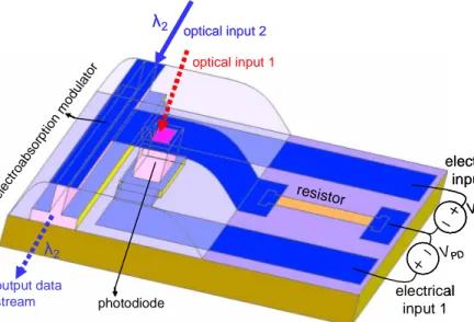
packet-diode that incorporates an InGaAsP/InP multiple quantum well structure optimized for large optical modulation over the C-band. The PD drives the EAM directly through a TaN thin-film resistor integrated in the vicinity of EAM and PD on the photonic chip as sketched in Fig. 1. There are two optical inputs to the switch; one onto the PD and one into the EAM. There are also two electrical inputs, the PD bias and the EAM bias. By using these inputs in various configurations, different aspects of the output data stream from the modulator can be controlled and a multitude of applications can be realized using the same physical construction. VPD VEAM electrical input 1 electrical input 2 resistor ele ctro abs orpt ion mod ulat or photodiode optical input 2 output data stream λ2 λ2 optical input 1 VPD VEAM electrical input 1 electrical input 2 resistor ele ctro abs orpt ion mod ulat or photodiode optical input 2 output data stream λ2 λ2 optical input 1
Fig. 1. A three-dimensional schematic of an integrated photonic switch incorporating a photodiode (PD) and an electroabsorption modulator (EAM). A thin film resistor is also integrated on the chip. There are two electrical voltage inputs (across the biasing pads of the EAM and the PD) and two optical inputs (onto the PD and into the EAM). There is one optical output (from the EAM).
3. Switch operation modes
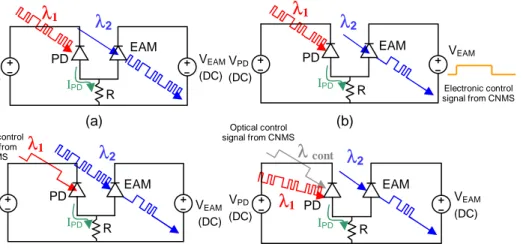
Figure 2(a) shows the basic operation for which the EAM and the PD are both reverse biased; there are also local bypass capacitors (not shown on the diagram) in parallel with each of the bias voltage sources. The bias across the EAM is set such that its quantum wells initially absorb the light coupled into the modulator waveguide. The presence of an input signal (i.e., an optical binary “1”) at λ1 on the PD results in a photocurrent, IPD, that generates a voltage
drop across the resistor, R, and consequently across the EAM. With this optically-induced voltage swing across the modulator, the absorption band edge shifts due to the quantum-confined Stark effect. This results in optical transmission through the EAM, leading to an optical binary “1” at the output. In this way, the input data is transferred bit-by-bit to the output, which converts the signal wavelength from λ1 to λ2.
In the second configuration as shown in Fig. 2(b), the EAM is electrically enabled when reverse biased and disabled when slightly forward biased by the respective enabling and disabling periods of a biasing electronic signal that comes from the central network management system (CNMS). With the enabling signal, the DC operating point of the EAM is set as in the basic switch operation and the optical switching action is observed in a similar way. However, if the disabling CNMS signal is present across the EAM, then the optical data transfer is completely blocked despite the optical input data steam that may be present at the PD. In this way, the electronic CNMS signal gates the optical switching and the optical wavelength conversion is packet switched electronically.
Fig. 2. Simplified circuit diagram of the integrated photonic switch operated in different configurations. (a) Basic optical switching operation: Both the EAM and the PD are reverse biased with a DC signal. Input data stream on the PD is transferred to the output, converting the wavelength, (b) Electrical packet switching: The EAM bias is a signal from the central network management system (CNMS) which enables/disables the switching node. The input data stream is seen at the output only when there is the enabling signal. (c) Optical packet switching: The optical control signal from the CNMS is incident on the PD. The data stream is coupled into the EAM this time, instead of a cw beam. The PD gates the input data stream. (d)
Simultaneous optical operations: Optical packet switching and wavelength conversion takes place simultaneously. Both the data and the control signal are incident on the photodiode and the optical input to the EAM is a continuous wave signal. EAM transmission occurs when both
λ1
λ1
Optical control signal from CNMS (a) (b) (c) (d) IPD VEAM VPD EAM PD (DC) (DC)λ
2 Rλ
2 IPD VEAM VPD EAM PD (DC) Electronic control signal from CNMS Rλ1
IPD VEAM VPD EAM PD (DC) (DC)λ
2 Rλ
2λ1
IPD VEAM VPD EAM (DC) Optical control signal from CNMS (DC)λ
cont PD Rtransferred to the output without modulation, so it can be modulated with some other stream of information in a preceding or a subsequent switch if desired.
In a fourth configuration, as shown in Fig. 2(d), the EAM and the PD are constantly reverse biased and a continuous-wave optical input is coupled into the EAM as in the basic case (Fig. 2(a)). Unlike the previous configurations, here two different optical beams are incident on the PD; one is the optical control signal from the CNMS and the other is the data signal. The “high” level in either of these signals does not generate enough photocurrent to create enough band-edge shift to result in transmission. Only when both signals are high is the data input transferred to the output.
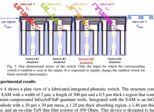
Thus, operating the same switch structure in different input configurations, a variety of network functionality can be achieved. Additionally, since this switch architecture is further scalable in two dimensions, it is possible to fabricate crossbar switches to offer space switching as well [9].These structures can then convert any set of input wavelengths to any set of output wavelengths available. However, to exploit such a structure fully in a network, it is important to reconfigure the switch rapidly and electronically. Figure 3 shows an example of how the basic switch architecture can be put in a one dimensional optical bus structure such that only the data stream for which the switch is enabled is observed at the output. In such a one-dimensional architecture, the ability to toggle between two switches and enable the desired one rapidly while disabling the other one is critical to proper bus operation.
Fig. 3. One dimensional arrays of the switch. Only the input for which the corresponding switch is enabled is seen at the output. It is important to rapidly change the enabled switch for better network functionality.
4. Experimental results
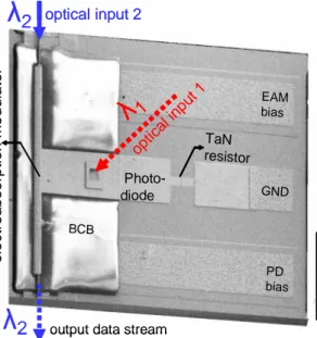
Figure 4 shows a plan view of a fabricated integrated photonic switch. The structure consists of an EAM with a width of 2 μm, a length of 300 μm and a 0.5 μm thick i-region that contains ten strain-compensated InGaAsP/InP quantum wells. Integrated with the EAM is an InGaAs photodiode with a 30 μm x 30 μm mesa, a 1.25 μm thick absorbing region, a 1.46 μm thick i-region, and an on-chip TaN thin film resistor of 450 Ohms. This device is designed to have a bandwidth of 2.5 GHz. The fabricated device exhibits a 3-dB switching bandwidth of 2.26 GHz, slightly reduced from the targeted value due to parasitic contact resistances [11].The photodiode and modulator are monolithically integrated using a new selective area growth technique [14]and a self-aligning polymer planarization and passivation technique [15, 16].
Photo-diode TaN resistor
λ
1
λ
2
e lectroa bsorp tion m odulato r optic al in put 1output data stream optical input 2 BCB PD bias GND EAM bias 1 0 0 µm
λ
2
Photo-diode TaN resistorλ
1
λ
2
e lectroa bsorp tion m odulato r optic al in put 1output data stream optical input 2 BCB PD bias GND EAM bias 1 0 0 µm
λ
2
Fig. 4. SEM picture of a fabricated photodiode-modulator switch.
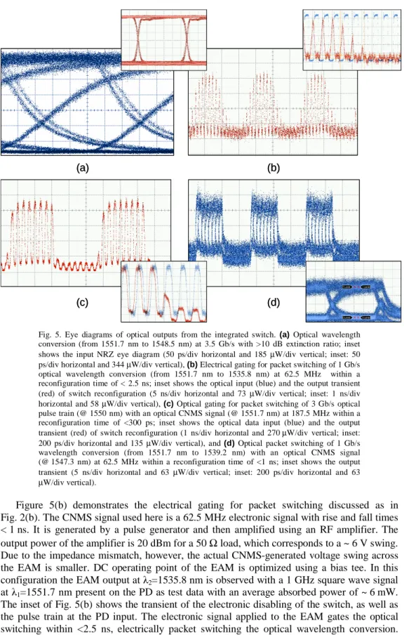
All-optical unconstrained wavelength conversion and dual-wavelength broadcasting have been demonstrated previously at data rates of 2.5 Gb/s [17] and 1.25 Gb/s [10], respectively, across the entire C-band. In Fig. 5 we present experimental results of the configurations described in Fig. 2. In these configurations PD and EAM are typically reverse biased with 15 V and 6 V DC signals, respectively, except for the configuration in Fig. 2(b), where a square wave CNMS signal is applied to the EAM.
Figure 5(a) shows a representative eye diagram taken from the switch output in non-return-to-zero (NRZ) format at 3.5 Gb/s, during the basic switch operation depicted in Fig. 2(a). In this eye diagram the extinction ratio is >10 dB for an absorbed optical power of ~10 mW. The inset shows the eye diagram of the NRZ data at the input. In this representative optical wavelength conversion, the input wavelength is λ1= 1551.7 nm and the output
wavelength is λ2= 1548.5 nm.
(a) (b)
(c) (d)
(a) (b)
(c) (d)
Fig. 5. Eye diagrams of optical outputs from the integrated switch. (a) Optical wavelength conversion (from 1551.7 nm to 1548.5 nm) at 3.5 Gb/s with >10 dB extinction ratio; inset shows the input NRZ eye diagram (50 ps/div horizontal and 185 μW/div vertical; inset: 50 ps/div horizontal and 344 μW/div vertical), (b) Electrical gating for packet switching of 1 Gb/s optical wavelength conversion (from 1551.7 nm to 1535.8 nm) at 62.5 MHz within a reconfiguration time of < 2.5 ns; inset shows the optical input (blue) and the output transient (red) of switch reconfiguration (5 ns/div horizontal and 73 μW/div vertical; inset: 1 ns/div horizontal and 58 μW/div vertical), (c) Optical gating for packet switching of 3 Gb/s optical pulse train (@ 1550 nm) with an optical CNMS signal (@ 1551.7 nm) at 187.5 MHz within a reconfiguration time of <300 ps; inset shows the optical data input (blue) and the output transient (red) of switch reconfiguration (1 ns/div horizontal and 270 μW/div vertical; inset: 200 ps/div horizontal and 135 μW/div vertical), and (d) Optical packet switching of 1 Gb/s wavelength conversion (from 1551.7 nm to 1539.2 nm) with an optical CNMS signal (@ 1547.3 nm) at 62.5 MHz within a reconfiguration time of <1 ns; inset shows the output transient (5 ns/div horizontal and 63 μW/div vertical; inset: 200 ps/div horizontal and 63 μW/div vertical).
Figure 5(b) demonstrates the electrical gating for packet switching discussed as in Fig. 2(b). The CNMS signal used here is a 62.5 MHz electronic signal with rise and fall times < 1 ns. It is generated by a pulse generator and then amplified using an RF amplifier. The output power of the amplifier is 20 dBm for a 50 Ω load, which corresponds to a ~ 6 V swing. Due to the impedance mismatch, however, the actual CNMS-generated voltage swing across the EAM is smaller. DC operating point of the EAM is optimized using a bias tee. In this configuration the EAM output at λ2=1535.8 nm is observed with a 1 GHz square wave signal
at λ1=1551.7 nm present on the PD as test data with an average absorbed power of ~ 6 mW.
The inset of Fig. 5(b) shows the transient of the electronic disabling of the switch, as well as the pulse train at the PD input. The electronic signal applied to the EAM gates the optical switching within <2.5 ns, electrically packet switching the optical wavelength conversion.
Note here that for basic switch operation bypass capacitors are required to provide a local low impedance “power supply” for the high-speed currents inside the devices, effectively isolating the high-speed device operation from external parasitics. Especially for high data rates, these capacitors have to be implemented on-chip to avoid parasitics. These bypass capacitors, however, also limit the rise time of the electronic CNMS signal to be delivered to the circuit, so care has to be taken in the design of these capacitors.
Figure 5(c) shows gating for packet switching with an optical control input, corresponding to the configuration summarized in Fig. 2(c). In this configuration both the PD and the EAM are constantly reverse biased. A 3 GHz square wave signal at λ2=1550 nm is coupled into the
EAM as test data. The optical CNMS signal, a square wave at 187.5 MHz with rise and fall times of 25 ps at wavelength λ1=1551.7, is incident on the PD with an average absorbed
power of ~ 6 mW. The optical control signal at λ1 gates the data at λ2. The inset of Fig. 5(c)
shows the transient of the switch being disabled, as well as the pulse train at the EAM input. Data transmission ceases when the optical CNMS signal disables the switch within a reconfiguration time of <300 ps.
Figure 5(d) demonstrates optically-controlled gating for packet switching together with wavelength conversion, corresponding to the configuration depicted in Fig. 2(d). In this case the PD and the EAM are constantly reverse biased. Incident on the PD are both the 1 Gb/s data stream at λ1=1551.7 nm and the optical CNMS signal, a square wave at 62.5 MHz at
λcont=1547.3 nm with ~7 mW of total average absorbed power on the PD. A continuous-wave
signal at λ2=1539.2 nm is coupled into the EAM and the output at λ2 is observed. The inset of
Fig. 5(d) shows the transition region in more detail. When the CNMS signal becomes low, the switch is disabled within a reconfiguration time of <1 ns and no data is observed at the output. Due to the nonlinearity of the EAM, the “high” level in either one of the two signals incident on the PD is not sufficient to generate enough photocurrent to drive the EAM and enable optical transmission through it. The two-level zero signal appearing between the packets is a result of the minor absorption change in the EAM due to the presence of the data signal alone in the absence of the CNMS signal.
5. Conclusion
In summary, we present a multifunctional integrated photonic switch that incorporates a monolithically integrated, surface-normal photodiode and a quantum well electroabsorption modulator. Integrated PD-EAMs make multifunctional photonic switches that exhibit low-power, high-speed operation with high extinction ratios across a wide wavelength band (full C band). The switches provide multiple network functions on a single chip. We demonstrate both optical wavelength conversion (at 3.5 Gb/s) and electrical packet switching (in < 2.5 ns) on the same optical channel using a single switch. Alternatively an optical control signal can be used for optical packet switching in < 300 ps without wavelength conversion and in < 1 ns with wavelength conversion. Our device characterization and modeling lead us to predict the feasibility of 10 Gb/s operation, by scaling down diode capacitances and thin film resistance, and minimizing parasitics [11].
Acknowledgments
The authors acknowledge Intel Corporation for the research funding, Dr. Jasper Hanberg of Intel GIGA ApS and OEpic Inc. for the epitaxial wafer growth, PTAP (funded by DARPA and NSF) for additional support and Thorlabs Inc. for the waveguide alignment setup. O.