EFFECTS OF FIELD PLATE ON THE MAXIMUM TEMPERATURE AND
TEMPERATURE DISTRIBUTION FOR GaN HEMT DEVICES
Dogacan Kara
Department of Mechanical Engineering, Middle East Technical University,
06531, Ankara, Turkey
Nazli Donmezer
Department of Mechanical Engineering, Middle East Technical University,
06531, Ankara, Turkey Talha Furkan Canan
Nanotechnology Research Center-NANOTAM, Bilkent University,
06800 Ankara, TURKEY
Ozlem Sen
Nanotechnology Research Center-NANOTAM, Bilkent University,
06800 Ankara, TURKEY
Ekmel Ozbay
Nanotechnology Research Center-NANOTAM, Bilkent University,
06800 Ankara, TURKEY
ABSTRACT
Field plated GaN high electron mobility transistors (HEMTs) are widely preferred amongst other GaN HEMT devices because of their ability to regulate electric field at high power densities. When operated at high power densities, GaN HEMTs suffer significantly from the concentrated heating effects in a small region called hotspot located closer to the drain edge of the gate. Although; the stabilizing effect of field plate on the electrical field distribution in HEMTs is known by researchers, its effect on temperature distribution and the hotspot temperature is still not studied to a greater extend. For this purpose, finite element thermal modelling of devices with different sizes of field plates are performed using the joule heating distribution data obtained from 2D electrical simulations. Results obtained from such combined model show that the existence of a field plate changes the electrical field, therefore the heat generation distribution within device. Moreover; increasing the size of the field plate has an effect on the maximum temperature at the hotspot region. The results are used to analyze these effects and improve usage of field plates for high electron mobility transistors to obtain better temperature profiles.
INTRODUCTION
The usage of AlGaN/GaN high electron mobility transistors (HEMTs) has surpassed other transistors due to their high radio frequency (RF) power densities [1, 2]. Due to opposite electrical charges of AlGaN and GaN layers in the device, electrons accumulate between these two layers creating a
charge density [6]. By applying a voltage difference between drain and source; electron flow is generated at the material interface (electron accumulated region), which is called two-dimensional electron gas (2DEG) region. To manage the electron flow through the 2DEG, gate voltage can be adjusted independently from the source voltage.
The working principle of GaN HEMTs, facilitated by the 2DEG formation and regulated by the gate voltage is both an advantage and a disadvantage for these devices [3-5] since gate voltage creates a resistance to the 2DEG electrons at drain side of the gate. This resistance causes sudden changes of the electrical field, thus high and localized Joule heating in the same region. This localized region is called the “hotspot” and can be treated as a nanoscale heat generation region [7]. This hotspot formation is considered as one of the reasons for device failure for GaN HEMTs [14]. Thus it is crucial to analyze and find factors that affect hotspot formation to improve GaN HEMT device performance and reliability.
On the other hand, the field plated GaN HEMTs are under intensive research to regulate sharp electric field variations in devices [8]. However; the effects of field plates on the hotspot region and device temperature are not studied enough to improve the system dynamics. The regulation effect of field plates on electric field may also scatter the localized heating from the hotspot since heat generation distribution is affected from the electric fields in the device.
Proceedings of the ASME 2016 Heat Transfer Summer Conference HT2016 July 10-14, 2016, Washington, DC, USA
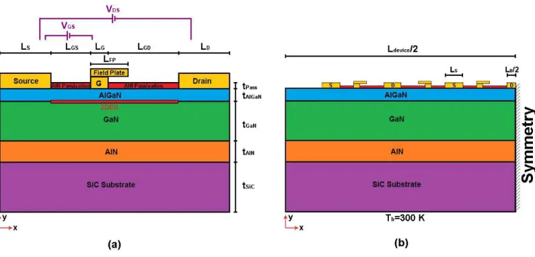
Figure 1. The schematic of GaN HEMT structure used in electrical (a) and thermal (b) simulations.
Past research on performance analysis of HEMTs are mainly categorized in two as: thermal performance and electrical performance studies. Except a few studies, many times thermal and electrical studies are decoupled from each other or not accurate and detailed enough [15, 16]. However, to find the true effects of field plate on the thermal performance of GaN HEMTs, a hybrid electrical and thermal analysis is necessary. The electrical outcomes of field-plated devices may affect the heat distribution and temperatures within the device, which can directly alter the device performance.
Sodan recently modeled the effects of source field plates on temperature for a single finger gate field plated GaN HEMTs on Silicon substrate [15]. However the main regulation effect of gate field plate is not studied to observe the heat generation scattering effect around hotspot region. In other words a systematic study between field plated and non-field plated devices was not performed in this study. Moreover the data was not used in independent thermal simulations to better evaluate the temperature distribution in devices where multiple fingers are present or with more complex geometries.
To answer some of these questions, in this study; first, electrical simulations for the same device with and without a field plate, are conducted to obtain the electrical performance of the devices. Then, based on the electrical performance, operating condition that give the same power output is selected for comparison purposes. Later, electrical simulations are
repeated at these operating conditions for the field plated and non-field plated devices to extract heating distributions. The effect of simulating single finger for electrical simulation instead of multiple fingers is negligible since while performing simulations it is observed that there is no superposition effect of each finger on one another contrary to the thermal simulations.
Using this data, thermal simulations are executed to see the thermal effects of field plates on devices. Thus, with these set of simulations, authors aim to observe the true thermal effects of field plates on maximum temperatures and temperature distribution of GaN HEMTs.
METHOD Device Structure:
The general structure of a GaN HEMT device is illustrated in Fig. 1 to clarify the device geometry. Figure 1(a) depicts the simpler model used in electrical simulations whereas Fig.1(b) illustrates the simplified thermal model used in this study. In both non-field plated and field plated devices, layers of; tPass=300nm AlN as passivation layer, tAlGaN=20 nm AlGaN, tGaN=2 µm GaN, tAlN=200 nm AlN and tSiC=125 µm SiC as substrate layer are used. Source, drain and gate metal contacts are defined as gold and their dimensions are defined as; LD=LS=34 µm source and drain lengths, LG=600nm gate length, LGS=1 µm gap between source and gate, LGD= 3.4 µm
gap between gate and drain, 150 µm gate width, 350 µm device length and width in a 6 finger device geometry. VG is the applied voltage between source and gate. The voltage applied between source and drain is defined as VDS. Simulations are conducted with 2D geometry assumption and symmetricity is used to ease the meshing and running processes. Number of triangular meshes used in this model is over 250 thousand to obtain precise results.
Electrical Simulations:
Detailed electrical simulations are necessary to obtain electric field and Joule heating distribution of GaN HEMT devices. In this study electrical simulations of a simple HEMT device shown in Fig. 1(a) are performed using Sentaurus TCAD: a computer simulation program used to develop and optimize electrical simulations for semiconductor processing technologies and devices.
For electrical simulations, exact device dimensions are used apart from source and drain lengths. Since electrons flow at 2DEG region, all the electrical field and heat generation occur in this region [9] and source and drain lengths do not have a significant effect on the simulation results, therefore these are taken as LG=LS=0.5 µm. Bottom temperature for device is set to Tb=300K and Ohmic resistances of RS=1 Ω and RD=103 Ω are defined to source and drain respectively. Gate is defined as a Schottky barrier with a barrier height of 1.48eV in electrical simulations.
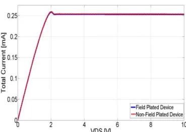
Both hydrodynamic and thermodynamic models are included in system physics and charge concentration of C=1.56x10¹³ C/μm is defined at AlGaN/GaN material interface [10]. Traps and doping concentrations for each material are introduced to the system as well. To simulate the behavior of devices with field plates a field plate of LFP=1200nm is added to the top-drain side of the gate as shown in the Fig. 1(a). All gate, drain and source are given Vini=0 V as initial condition. To run the simulations, gate voltage is ramped to VG=-1 V and then drain voltage is increased to VDS=10 V. The I V curve obtained for the field plated and non-field plated devices are shown in Fig. 2.
Figure 2. Total current vs. VDS graph for non-field plated and field plated GaN HEMTs
The heating distribution obtained from the electrical simulations is used to calculate the net absolute heat flux data for both non-field plated and field plated devices under defined operating conditions. This data is later used as a boundary heat generation at thermal simulations.
Thermal Simulations:
Thermal simulations are conducted for the structure given in Fig. 1(b) using COMSOL Multiphysics, which is a finite analysis simulation program. As shown in Fig. 1(b) system geometry is generated in 2D as 3 fingers with insulation boundary condition at the cut line to simulate the 6-finger device. Actual device dimensions are used to create the thermal model for simulation.
Material properties are taken from COMSOL Library and thermal conductivities are defined manually as; for gold contacts kAu=3.18 W/cm*K, kAlGaN,GaN=(T/300)-0.5 W/cm*K for GaN and AlGaN layers, kSiC=3.95*(T/293)-1.29 for SiC substrate [11]. Thermal conductivities of GaN, AlGaN and SiC are defined as temperature dependent to obtain more precise results. AlN thermal conductivity is used as the predefined value of COMSOL for this material and thermal boundary resistance (TBR) between GaN and SiC is taken as 3.3x10⁻⁸ m2*K/W [12]. Thermal boundary conditions for this device are defined as natural convection over the top and left boundaries of the device at Tinf=25 °C, P=1 atm, insulation condition at the right boundary due to symmetricity and temperature boundary condition at the bottom surface as Tb=300K. Heat generation data obtained from electrical simulation is imported as 1D heat flux data and defined at the 2DEG region as boundary heat source for each finger.
RESULTS AND DISCUSSION
To observe the thermal effects of field plates on devices operating condition of VG=-1 V and VDS=10 V is used. Although at high power densities, adding field plate to device decreases the current, thus; decreases power density and heat generation [13] at the given operating conditions both the field plated and non-field plate devices performed similarly resulting with power outputs of 2.53W/mm and 2.51W/mm, respectively. By using almost identical power densities it is possible to analyze the field plate’s effects on the distribution of Joule heating in devices.
The effect of field plate on electrical field distribution around the hotspot can be seen from Fig. 3. As it was expected
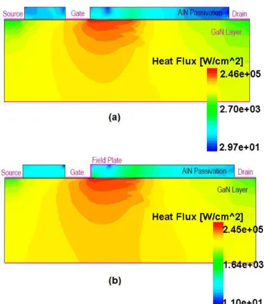
[8], field plate regulates the electrical field within the 2DEG and decreases the intensity of electrical field both in the 2DEG region and the hotspot region. Similar to the electrical field, heat flux data can be obtained from electrical simulations. Heat flux data obtained from simulations is presented in Fig. 4 for non-field plated and field plated GaN HEMTs. The effect of field plates on heat flux is evident in Fig.4, since heat flux is more spread within the device in field-plated devices compared to non-field plated devices. In other words, due to the same power density, both devices generate the same amount of heat but non-field plated device dissipates this heat from a more localized region, compared to field plated GaN HEMT.
(a) (b) Figure 3. Electric field distribution for non-field plated (a) and field plated (b) GaN HEMTs
Figure 4. Heat flux distribution for non-field plated (a) and field plated (b) GaN HEMTs
By summing the absolute heat flux data 0.5 nm above and below the 2DEG region; one can obtain the net heat generated inside the 2DEG region and use this as a 1D heat generation distribution with negligible data loss. This 1D data can be used in thermal simulations of devices to represent heat generation distribution of devices. The heat generation distributions shown in Fig. 5 show that although the total heat generation for devices is equal, distribution of this generation has different characteristics. Non-field plated device has most of this generation localized in 1.5 µm region, on the other hand field plated GaN HEMT device has a more scattered generation data as shown in Fig. 5. Localized heat generation in the non-field plated device increases the hotspot temperature since dissipation of the heat generated in that micro/nanoscale region by conduction becomes difficult. This high temperature in the AlGaN/GaN interface may lead to burnout in GaN HEMT devices.
Figure 5. Heat generation distribution from 2DEG region for non-field plated and field plated GaN HEMTs
To observe the effect of field plate on hotspot temperature and temperature distribution in the device, AlGaN/GaN material interface is investigated and temperature distribution graph for a six-finger device is obtained. Due to symmetricity condition, plots for 3 fingers are given in Fig. 6 for non-field plated and field plated GaN HEMTs respectively.
Figure 6. Temperature distribution at AlGaN/GaN interface for non-field plated and field plated GaN HEMTs
A temperature peak for each finger can be seen in the Fig. 6. The top of each peak corresponds to the hotspot regions. The highest temperatures are observed at innermost fingers since heat dissipation from these regions are harder compared to others. Maximum temperature at the hotspot region for non-field plated device is observed as 364.2°C, on the other hand, the maximum temperature for field plated device is 358.3°C. This difference of 6°C is significant, especially in a device with a relatively low power density of 2.51W/mm. Also peaks are less steep for field-plated device compared to field plated, meaning that field plate also has a scattering effect on temperature distribution. With increasing power densities, this effect may increase but as discussed earlier, adding field plate to devices with high power density has a negative effect on
power density itself, creating an argumentative situation due to the decreased heat generation.
CONCLUSION
This study analyses the effects of field plates for GaN HEMT devices on power density output, electrical field, heat flux, heat generation and temperature distributions and maximum temperature at the device for operating conditions at -1V gate voltage and 10V drain voltage. Simulation techniques and outcomes have been taken into account and interconnections between electrical and thermal properties have been discussed. The overall effects of field plates can be put in order as:
Field plate regulates the electric field distribution in the device and scatters it from a localized region to a larger area.
This regulation effect on electrical field also affects heat generation distribution at the 2DEG region.
The device without field plate generates high amounts of heat at a local 1 µm region, on the other hand, field plated device generates same amount of heat in a scattered trend.
Localized heat generation results in smaller hotspot region with higher maximum temperature for non-field plated GaN HEMT device.
NOMENCLATURE
C charge concentration LD drain length
LFP field plate length
LGD distance between gate and drain LG gate length
LGS distance between source and gate
LS source length
VDS voltage between source and drain VG gate voltage
Vini initial voltage RS source resistance RD drain resistance Tb base temperature Tinf room temperature
kAlGaN/GaN AlGaN and GaN thermal conductivity kAu Au thermal conductivity
kSiC SiC thermal conductivity tAlGaN AlGaN thickness tAlN AlN thickness tGaN GaN thickness tPass passivation thickness tSiC SiC thickness
ACKNOWLEDGMENTS
The authors would like to acknowledge Mohammad Azarifar, Cemil Kayış, and Didem Cansu İlhan for their valuable support. This work was supported by the METU-BAP (Grant no: BAP-08-11-2015-028) and the TUBITAK (Grant no: 115E756).
REFERENCES
1. Hikita, M., et al., AlGaN/GaN power HFET on
silicon substrate with source-via grounding (SVG) structure. Electron Devices, IEEE Transactions on,
2005. 52(9): p. 1963-1968.
2. Sangmin, L., et al. Reliability assessment of
AlGaN/GaN HEMT technology on SiC for 48V applications. in Reliability Physics Symposium, 2008. IRPS 2008. IEEE International. 2008.
3. Vitanov, S., et al., High-temperature modeling of
AlGaN/GaN HEMTs. Solid-State Electronics, 2010.
54(10): p. 1105-1112.
4. Park, J., M.W. Shin, and C.C. Lee, Thermal modeling
and measurement of GaN-based HFET devices.
Electron Device Letters, IEEE, 2003. 24(7): p. 424-426.
5. Pengelly, R.S., et al., A Review of GaN on SiC High
Electron-Mobility Power Transistors and MMICs.
Microwave Theory and Techniques, IEEE Transactions on, 2012. 60(6): p. 1764-1783.
6. D.-P. Wang, C.-C. Wu, and C.-C. Wu, “Determination of polarization charge density on interface of AlGaN∕GaN heterostructure by electroreflectance,”
Appl. Phys. Lett., vol. 89, no. 16, p. 161903, 2006.
7. Donmezer, F., Multiscale electro-thermal modeling of
AlGaN/GaN heterostructure field effect transistors.
2013.
8. V. Palankovski, S. Vitanov, G. Cap, and K. Mc,
“Field-Plate Optimization of AlGaN / GaN HEMTs,”
pp. 107–110.
9. C. Network and I. Sharing, “Naval Postgraduate,”
Security, no. December, 2009.
10. a Venkatachalam, W. T. James, and S. Graham, “Electro-thermo-mechanical modeling of GaN-based
HFETs and MOSHFETs,” Semicond. Sci. Technol.,
vol. 26, p. 085027, 2011.
11. F. Cappelluti, M. Furno, A. Angelini, F. Bonani, M. Pirola, and G. Ghione, “On the substrate thermal
optimization in SiC-based backside-mounted high-power GaN FETs,” IEEE Trans. Electron Devices,
vol. 54, pp. 1744–1752, 2007.
12. Donmezer, N. and S. Graham, The impact of
of AlGaN/GaN HFETs. Electron Devices, IEEE
Transactions on, 2014. 61(6): p. 2041-2048.
13. C.-Y. Chiang, H.-T. Hsu, and E. Y. Chang, “Effect of
Field Plate on the RF Performance of AlGaN/GaN HEMT Devices,” Phys. Procedia, vol. 25, pp. 86–91,
2012.
14. J. a. F. Perez, “Thermal Study of a GaN based HEMT,” no. September, p. 229, 2012.
15. V. Šodan, H. Oprins, S. Stoffels, M. Baelmans, I. De Wolf, S. Member, A. Thermal, and A. Gan,
“Influence of Field-Plate Configuration on Power Dissipation and Temperature Profiles in AlGaN / GaN on Silicon HEMTs,” vol. 62, no. 8, pp. 2416– 2422, 2015.
16. G. Kurt, A. Toprak, O. A. Sen, and E. Ozbay, “Effect of Field Plate Length on Power Performance of GaN Based HEMTs,” pp. 247–250.