ATOMIC LAYER DEPOSITION OF METAL
OXIDES ON SELF-ASSEMBLED PEPTIDE
NANOFIBER TEMPLATES FOR
FABRICATION OF FUNCTIONAL
NANOMATERIALS
a thesis submitted to
the graduate school of engineering and science
of bilkent university
in partial fulfillment of the requirements for
the degree of
master of science
in
materials science and nanotechnology
By
Hamit Eren
August 2016
ATOMIC LAYER DEPOSITION OF METAL OXIDES ON SELF-ASSEMBLED PEPTIDE NANOFIBER TEMPLATES FOR FABRI-CATION OF FUNCTIONAL NANOMATERIALS
By Hamit Eren August 2016
We certify that we have read this thesis and that in our opinion it is fully adequate, in scope and in quality, as a thesis for the degree of Master of Science.
Mustafa ¨Ozg¨ur G¨uler(Advisor)
Aykutlu Dˆana
Macit ¨Ozenba¸s
Approved for the Graduate School of Engineering and Science:
Levent Onural
ABSTRACT
ATOMIC LAYER DEPOSITION OF METAL OXIDES
ON SELF-ASSEMBLED PEPTIDE NANOFIBER
TEMPLATES FOR FABRICATION OF FUNCTIONAL
NANOMATERIALS
Hamit Eren
M.S. in Materials Science and Nanotechnology Advisor: Mustafa ¨Ozg¨ur G¨uler
August 2016
There are mainly two basic approaches in nanostructured materials synthesis. The first one is the top-down approach and requires material removal from a bulk substrate material by chemical, physical, mechanical or thermal means; acid etching, focused ion milling, and laser ablation are among these top-down syn-thesis techniques. It is a straightforward – albeit poor in material architecture control – method that has established its niche in today’s high-volume CMOS transistor fabrication technology which already produces single-digit nanometer-scale device features. On the other hand, bottom-up approach exploits fine-tuned materials assembly. Bottom-up approach is realized via direct self-assembly of target nanostructures or material growth on synthetic or natural nanotemplates. Bottom-up nanostructured materials synthesis offers considerably wider spec-trum of achievable material architectures and structural hierarchies. Synthesis of nanostructured materials on self-assembled soft nanotemplates is of significant importance because many biological systems utilize this very similar approach to construct complex biomolecule-templated materials. Peptide amphiphile (PA) molecules with their intrinsic property to self-assemble into nanostructures such as fibers, present a versatile tool in inorganic material templating. PAs were used as soft templates in several studies for fabrication of nanoscale inorganic materi-als. Most of these studies are focused on in-solution material deposition on the surface of a template. Even though this approach allows successful material depo-sition, precise control over material thickness, uniformity, and high conformality is difficult to achieve in a repeatable manner. In order to circumvent this chal-lenge, in this thesis, atomic layer deposition (ALD) technique was deployed for conformal coating of PA nanonetwork templates. ALD involves low-temperature
iv
iterative vapor-phase material deposition in a self-limiting fashion. In each de-position half-cycle, Ti- or Zn- containing volatile metalorganic complexes form a self-limiting uniform monolayer that consequently reacts with water vapor (H2O)
as an oxygen precursor in the subsequent process half-cycle. As each half-cycle is separated with purge cycles, no gas-phase reactions occurs and material growth proceeds only with surface chemical ligand-exchange reactions. ALD approach allowed obtaining TiO2 or ZnO nanonetworks with tunable wall thickness and
ultimate conformality. Obtained metal oxide-peptide hybrid materials were fur-ther treated differently. In the case of TiO2, organic template was removed upon
calcination at 450◦C, a temperature at which amorphous titania transforms to anatase form. ZnO-peptide hybrid materials on the other hand, did not undergo any thermal processing, as ZnO already grows in wurtzite crystalline form dur-ing ALD process. In principle, nanostructured anatase TiO2 and wurtzite ZnO
are wide bandgap semiconductors which can be used as photoanode materials. Nanostructured anodic materials still attract a great interest as the matter at nanoscale regimes can provide considerable enhancement in charge carrier sepa-ration, charge carrier transport, and active surface area. Here we demonstrate the fabrication of nanostructured TiO2 and ZnO on self-assembled soft templates. As
a proof of principle, we utilized semiconducting TiO2 and ZnO in assembly of dye
sensitized solar cells and studied material thickness effect on device performance parameters such as open circuit voltage (Voc), short circuit current (Jsc), and fill factor. Three sets of nanostructured photoanodes with different TiO2
depo-sition cycles (100, 150, and 200) and ZnO depodepo-sition cycles (100, 125 and 150) were fabricated. TiO2 and ZnO nanonetworks in photoanodes form a system of
interconnected nanotubes, which can facilitate electron transfer. Moreover, these networks are porous high-surface area materials and they can drastically increase number of sensitizer molecules attached to the semiconductor material surface.
Keywords: Atomic layer deposition, TiO2, ZnO, self-assembly, peptide nanofiber,
¨
OZET
KEND˙IL˙I ˘
G˙INDEN D ¨
UZENLENEN PEPT˙IT NANOL˙IF
KALIPLAR VE ATOM˙IK KATMAN KAPLAMA
Y ¨
ONTEM˙IYLE FONKS˙IYONEL NANOMALZEME
¨
URET˙IM˙I
Hamit Eren
Malzeme Bilimi ve Nanoteknoloji B¨ol¨um¨u, Y¨uksek Lisans Tez Danı¸smanı: Mustafa ¨Ozg¨ur G¨uler
A˘gustos 2016
Nanomalzeme sentez y¨onteminde ba¸slıca iki temel yakla¸sım vardır. ˙Ilki yukarıdan-a¸sa˘gıya bir yakla¸sım ve daha y¨uksek hacimli malzemeden kimyasal, fiziksel, mekanik ya da termal yollarla malzeme uzakla¸stırılmasını gerektirir; asit a¸sındırma, odaklanmı¸s iyonlama, lazer ablasyon bu yukarıdan-a¸sa˘gıya sen-tez teknikleri arasında yer almaktadır. Bu nano yapılı malzeme sensen-tez y¨ontemi her ne kadar malzemenin yapı kontrol¨unde zayıf da olsa, basit bir y¨ontemdir. G¨un¨um¨uz¨un y¨uksek hacimli CMOS transist¨or ¨uretme teknolojisinde yerini al-maktadır. Ote yandan, a¸sa˘¨ gıdan-yukarıya yakla¸sım ince ve uygun ayarlanmı¸s k¨u¸c¨uk malzeme bloklarını kullanır. A¸sa˘gıdan-yukarıya yakla¸sım do˘grudan hedef nanoyapıların kendili˘ginden d¨uzenlenerek bir araya gelmesi veya sen-tetik veya do˘gal nanokalıpların kullanılarak do˘grudan malzeme b¨uy¨utme yoluyla ger¸cekle¸stirilmektedir. A¸sa˘gıdan-yukarıya malzeme sentez y¨ontemi hem elde edinmek istenen malzeme yapılar hem de yapısal hiyerar¸sileri olu¸sturmak i¸cin olduk¸ca geni¸s bir yelpaze sunar. Bir¸cok biyolojik sistem karma¸sık kalıp ta-banlı biyomolek¨ul malzeme olu¸sturmak i¸cin benzer bir yakla¸sım kullandı˘gından bu y¨ontemle nano yapılı malzemelerin sentezi b¨uy¨uk ¨onem ta¸sımaktadır. Pep-tit amfifil (PA) molek¨ullere ¨ozg¨un olan bir araya kendili˘ginden d¨uzenlenerek olu¸san yapılar oldu˘gundan, anorganik malzeme kalıplamada ¸cok y¨onl¨u bir ara¸c sunmaktadır. PA malzemeler nano ¨ol¸cekli anorganik malzemelerin ¨uretimi i¸cin ¸ce¸sitli ¸calı¸smalarda, yumu¸sak kalıplar olarak kullanılmı¸stır. Bu ¸calı¸smaların ¸co˘gunda kalıp y¨uzeyi ¨uzerinde malzeme birikimi sol¨usyon tabanlı biriktirme y¨ontemi ¨uzerinde yo˘gunla¸smı¸stır. Her ne kadar bu y¨ontemle ba¸sarılı malzeme biriktirme ger¸cekle¸stirmek m¨umk¨un olsa da, malzeme kalınlı˘gının hassas kon-trol¨un¨u, malzeme kalınlı˘gı b¨ut¨unl¨u˘g¨un¨u ve y¨uksek konformlu˘gunu tekrarlanabilir
vi
bir ¸sekilde elde etmek zordur. Bu zorlu˘gu a¸smak i¸cin, bu tezde, atomik katman biriktirme (ALD) tekni˘gi ile PA nanoa˘g kalıpların ¨uzerine konformal bir ¸sekilde malzeme b¨uy¨utme ger¸cekle¸stirildi. ALD buhar fazından kendini sınırlayan bir bi¸cimde d¨u¸s¨uk sıcaklıkta tekrarlı bir ¸sekilde malzeme b¨uy¨utme y¨ontemidir. Her bir yarım d¨ong¨ude, Ti- ya da Zn- i¸ceren u¸cucu metalorganik kompleksler kendi kendini sınırlayan homojen tek tabaka olu¸sturur ve hemen arkasından, bir oksijen ¨
onc¨us¨u olarak su buharı (H2O) ile reaksiyona girerek yarım d¨ong¨uy¨u tamamlar.
Her bir yarım d¨ong¨u arası temizleme d¨ong¨uleri ile ayrıldı˘gından, gaz fazında reak-siyonlar ger¸cekle¸smez. Malzeme b¨uy¨utmesi yalnızca y¨uzeydeki kimyasal ligand-yer de˘gi¸stime reaksiyonları ile ger¸cekle¸sir. ALD yakla¸sımı ayarlanabilir duvar kalınlı˘gı ve y¨uksek kalıp konformalitesine sahip TiO2 veya ZnO nanoa˘gların
olu¸smasını m¨umk¨un kıldı. Elde edilen metal oksit-peptit hibrid malzemeler farklı i¸slemlere tabi tutuldu. TiO2 malzeme i¸cerisinde bulunan organik kalıp 450◦C
sıcaklıkta uzakla¸stırılmı¸stır. Bu sıcaklık TiO2 malzemesini amorf yapısından
anataz formuna d¨on¨u¸st¨urm¨u¸st¨ur. ZnO malzemesi ALD i¸slemi sırasında hekzago-nal kristal ¸seklinde b¨uy¨ud¨u˘g¨unden, ZnO-peptit hibrid malzeme i¸cin herhangi bir ısıl i¸slem uygulanmadı. Prensip olarak, geni¸s bant aralıklı yarı iletkenler olan anataz forma sahip TiO2 ve hekzagonal yapıya sahip ZnO fotoanot malzemeleri
olarak kullanılabilirler. Nanoyapılı anodik malzemeler y¨uk ta¸sıyıcı ayırma, y¨uk ta¸sıyıcı ta¸sıma ve aktif y¨uzey alanınlarında ¨onemli bir artı¸s sa˘gladı˘gından hala b¨uy¨uk bir ilgi ¸cekmektedir. Burada kendili˘ginden d¨uzenlenmi¸s yumu¸sak kalıplar ¨
uzerinde b¨uy¨ut¨ulm¨u¸s nano yapılı TiO2ve ZnO malzeme ¨uretimini g¨ostermekteyiz.
Y¨ontemin kavramsal kanıtı olarak, TiO2 ve ZnO yarı iletken malzemeler boya
duyarlı g¨une¸s h¨ucrelerinde kullanıldı. De˘gi¸sen malzeme kalınlı˘gının a¸cık devre gerilimi (Voc), kısa devre akımı (Jsc) ve dolgu fakt¨or¨u gibi h¨ucre parametreleri ¨
uzerinde etkisi olabilece˘ginden g¨une¸s h¨ucreleri ¨uzerindeki performansları ince-lendi. Farklı TiO2 (100, 150 ve 200) ve ZnO (100, 125 ve 150) katman d¨ong¨ulerine
sahip ¨u¸c grup fotoanot malzeme ¨uretildi. Fotoanot i¸cerisindeki TiO2 ve ZnO
nanoa˘glar elektron transferini kolayla¸stıracak ¸sekilde birbirine ba˘glı bir nanot¨up sistemi olu¸sturdu. Ayrıca, bu a˘glar, g¨ozenekli, y¨uksek y¨uzey alanlı malzemeler olup ve yarı iletken malzeme y¨uzeyine tututan boya molek¨ullerinin sayısını b¨uy¨uk ¨
ol¸c¨ude artırabilir.
Anahtar s¨ozc¨ukler : Atomik katman kaplama, TiO2, ZnO, kendili˘ginden
Acknowledgement
First and foremost I would like to express my sincere gratitude to my supervisor Dr. Mustafa ¨Ozg¨ur G¨uler for his constant guidance and experience transfer and support that allowed me to work in many different research projects which ex-tended my knowledge and vision. I am sincerely grateful to Dr. Necmi Bıyıklı, Dr. Ali Kemal Okyay, and Dr. Tamer Uyar for their active collaborations and fruitful discussions.
I would like to acknowledge all the professors, instructors, engineers, and graduate students at UNAM and Institute of Materials Science and Nanotechnology. Es-pecially, I would like to express most sincere thanks to all the members of Bıyıklı group, G¨uler group, Okyay group, and Uyar group. I would like to acknowledge The Scientific and Technological Research Council of Turkey (T ¨UB˙ITAK) for supporting 112M578 grant.
Finally, I am immeasurably indebted to my family which has constantly sup-ported and encouraged me during my M.Sc. study.
Contents
1 Introduction 1
2 Theoretical Background and Literature Overview 4
2.1 Atomic Layer Deposition (ALD) . . . 4
2.1.1 Mechanism . . . 6
2.1.2 Growth Modes of ALD . . . 9
2.1.3 Choice of Precursors . . . 11
2.1.4 ALD Window . . . 12
2.1.5 Atomic Layer Deposition of Metal Oxides . . . 13
2.2 Self-Assembled Peptide Nanostructures . . . 16
2.2.1 Peptide Chemistry . . . 16
2.2.2 Solid Phase Peptide Synthesis . . . 16
2.2.3 Self-Assembly of Peptides . . . 19
CONTENTS ix
3 Experimental Details 24
3.1 Materials and Reagents . . . 24
3.2 Peptide Synthesis and Characterization . . . 24
3.3 Photoanode Fabrication and Characterization . . . 26
3.4 Atomic Layer Deposition of TiO2 and ZnO . . . 27
3.5 Solar Cell Assembly and Characterization . . . 27
3.6 ICP-MS Measurements . . . 28
4 Results and Discussion 29
List of Figures
2.1 Cross-sectional SEM image of 300 nm Al2O3 film on a Si wafer
with a trench structure . . . 5
2.2 Simplified mechanism for one unit ALD reaction cycle . . . 7
2.3 The chemisorption mechanisms possible in ALD . . . 10
2.4 Simplified schemes of the different growth modes in ALD with increasing number of reaction cycles n . . . 11
2.5 Conceptual illustration of an ALD process temperature window with respect to the substrate processing temperature. . . 13
2.6 Condensation of two amino acids to form a dipeptide through a peptide bond . . . 17
2.7 The principles of SPPS . . . 18
2.8 Self-assembly of PA molecules into a cylindrical micelle. . . 22
3.1 Structural formula of lauryl-VVAGK-Am peptide amphiphile . . . 25
3.2 Liquid chromatogram of lauryl-VVAGK-Am peptide amphiphile . 25
LIST OF FIGURES xi
4.1 Fabrication of nanostructured peptide template . . . 30
4.2 SEM micrographs of TiO2 nanonetworks after calcination . . . 30
4.3 TEM micrographs TiO2 coated nanofibers after calcination . . . . 31
4.4 EDX spectra of as-synthesized a) 100-, b) 150- and c) 200-cycle TiO2 36
4.5 EDX spectra of a) 100-, b) 125- and c) 150-cycle ZnO . . . 37
4.6 XRD spectra of as-synthesized 100-, 150- and 200-cycle TiO2 . . . 38
4.7 Raman spectra of as-synthesized 100-, 150- and 200-cycle TiO2 . . 38
4.8 XRD spectra of 100, 150, and 200-cycle TiO2 . . . 39
4.9 Raman spectra of 100, 150, and 200-cycle TiO2 . . . 39
4.10 SEM micrographs of a) 100-cycle, b) 125-cycle, and c) 150-cycle ZnO nanonetworks . . . 40
4.11 TEM micrographs a) 100-cycle, b) 125-cycle, and c) 150-cycle ZnO coated nanofibers . . . 40
4.12 XRD spectra of 100, 125, and 150-cycle ZnO . . . 41
4.13 Raman spectra of 100, 125, and 150-cycle ZnO . . . 41
4.14 Cross-sectional view of nanostructured TiO2 and ZnO photoanodes 42
4.15 Tauc plots of as-synthesized TiO2 . . . 42
4.16 Tauc plots of calcined TiO2 . . . 43
4.17 EDX spectra of calcined a) 100-, b) 150- and c) 200-cycle TiO2 . . 44
LIST OF FIGURES xii
4.19 J-V curves of 100, 150 and 200-cycle TiO2 devices . . . 45
4.20 J-V curves of 100, 125 and 150-cycle ZnO devices . . . 46
4.21 Ru calibration line . . . 46
4.22 Ti calibration line . . . 46
List of Tables
2.1 List of non-covalent interactions . . . 19
4.1 N719 sensitizer amounts adsorbed by TiO2 . . . 34
4.2 N719 sensitizer amounts adsorbed by ZnO . . . 34
Chapter 1
Introduction
There are mainly two basic approaches in nanostructured materials synthesis. The first one is the top-down approach and requires material removal from a bulk substrate material by chemical, physical, mechanical or thermal means; acid etching, focused ion milling, and laser ablation are among these top-down syn-thesis techniques. It is a straightforward – albeit poor in material architecture control – method that has established its niche in today’s high-volume CMOS transistor fabrication technology which already produces single-digit nanometer-scale device features.
On the other hand, bottom-up approach exploits fine-tuned materials assem-bly. Bottom-up approach is realized via direct self-assembly of target nanos-tructures or material growth on synthetic or natural nanotemplates. Bottom-up nanostructured materials synthesis offers considerably wider spectrum of achiev-able material architectures and structural hierarchies. Synthesis of nanostruc-tured materials on self-assembled soft nanotemplates is of significant importance because many biological systems utilize this very similar approach to construct complex biomolecule-templated materials.
Peptide amphiphile (PA) molecules with their intrinsic property to self-assemble into nanostructures such as fibers, present a versatile tool in inorganic material templating. PAs were used as soft templates in several studies for fabri-cation of nanoscale inorganic materials. Template assisted synthesis of functional nanomaterials, such as nanotubes, nanorods, and nanowires has attracted great attention from researchers in the past decade. As a striking example, ALD-coated materials such as tissue have been demonstrated as an efficient method to enhance the water resistance. As a result of burning out the tissue, a residue of Al2O3 is formed, which carries a replication of original tissue with fiber-like
structure. As intrigued by this example, in this study, we attempted to fabricate functional nanostructures based on self-assembled peptide amphiphile templates by exploiting ALD, targeting applications in dye-sensitized solar cells (DSSCs).
ALD, a special type of chemical vapor deposition (CVD) technique, is a very effective and unique method for deposition of high-quality organic/inorganic thin films with thickness control down to a fraction of monolayer. Self-assembled peptide amphiphile templates offer the advantages of low-cost, high flexibility in morphology, and sufficient surface reactivity with ALD precursors. Due to its porosity and high surface area, template assisted synthesis of such nanomaterials can be used in many fields including wearable electronics, biological and chemical sensing, energy generation, and storage.
Template assisted synthesis strategy is a unique methodology to construct materials in which physical dimensions can be precisely tailored. Conformal du-plication of the morphologies by using self-assembled peptide templates and ALD pave the way for the formation of sophisticated functional nanostructures. In this thesis, high surface area peptide aerogel networks were prepared on conductive glass substrates, FTO. ALD was used to deposit aerogel template with superior conformity and uniformity with various thicknesses of TiO2 and ZnO and with
sub-nanometer precision.
In principle, nanostructured anatase TiO2 and wurtzite ZnO are wide bandgap
semiconductors which can be used as photoanode materials. Nanostructured anodic materials still attract a great interest as the matter at nanoscale regimes
can provide considerable enhancement in charge carrier separation, charge carrier transport, and active surface area. The TiO2- and ZnO-coated aerogel templates
were utilized as photoanodes in DSSCs.
Impact of metal oxide layer thickness on device performance was evaluated. Three sets of nanostructured photoanodes with different TiO2 deposition cycles
(100, 150, and 200) and ZnO deposition cycles (100, 125 and 150) were fabricated. TiO2 and ZnO nanonetworks in photoanodes form a system of interconnected
nanotubes, which can facilitate electron transfer. Moreover, these networks are porous high-surface area materials and they can drastically increase number of sensitizer molecules attached to the semiconductor material surface.
This thesis is organized as follows. Following this brief introduction, Chapter 2 presents a theoretical background and literature overview for ALD and its basic principles. Growth modes of ALD, choice of precursors, ALD window, and deposition of common metal oxides, such as TiO2, Al2O3, and ZnO with their
reaction mechanisms are reviewed in this chapter as well. In the second part of the Chapter 2, self-assembled peptide nanostructures are overviewed. Peptide chemistry, solid phase peptide synthesis, and non-covalent interactions between peptide molecules are also introduced in this chapter.
Detailed information regarding to the experimental procedure, i.e., materials and reagents, peptide synthesis and characterization, photoanodes fabrication and characterization, atomic layer deposition of TiO2 and ZnO, solar cell assembly
and characterization, and lastly ICP-MS measurements, is provided in Chapter 3.
Chapter 4 discusses the results of fabrication of functional nanostructures based on self-assembled peptide amphiphile templates by exploiting ALD and targeting applications in dye-sensitized solar cells (DSSCs).
Finally, Chapter 5 concludes with a summary of achievements and future re-search directions.
Chapter 2
Theoretical Background and
Literature Overview
2.1
Atomic Layer Deposition (ALD)
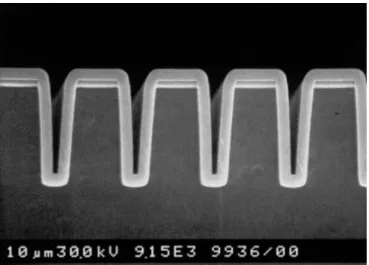
Atomic layer deposition (ALD), a special type of chemical vapor deposition (CVD) technique, is a very effective and unique method for the deposition of high-quality organic/inorganic thin films with thickness precision down to frac-tions of a monolayer [2–5]. It has the capability to deposit surfaces of arbitrary topography and complex stuctures with high conformality and uniformity. Com-pared to other CVD techniques, ALD proceeds in a cyclic manner, where the reactants are pulsed onto the substrate surface one at a time, segregated by purg-ing and/or evacuation periods which help remove excess reactants and reaction by-products. This ensures that no gas-phase reactions take place and material growth is controlled via self-limiting chemical ligand-exchange reactions on the surface. The characteristic features of ALD distinguishing it from other CVD methods are successive, self-terminating gas-solid reactions for fabrication of uni-form, conformal, dense, and pinhole-free thin layers either on high aspect ratio structures or flat substrates. Figure 2.1 reveals the superior conformality on high aspect ratio trenched substrates [6].
Figure 2.1: Cross-sectional SEM image of 300 nm Al2O3 film on a Si wafer with a
trench structure. (Reprinted with permission from ref [6]. Copyright 1999 John Wiley & Sons.)
ALD is not a new or recent technique. Over the years, it was named with many different names, such as molecular layering, molecular layer epitaxy, atomic layer growth, and atomic layer epitaxy [7–9]. Even though the origin of ALD is controversial, according to most sources, its roots date back to 1950s. The very first concept of ALD was proposed and published as early as 1952 in a Ph.D. thesis by V. B. Aleskovskii in the Soviet Union [10]. Later, Prof. Aleskovskii and Prof. S.I. Koltsov published the principle of ALD under the name of Molecular Layering in the Soviet Union in 1965 [11]. These two reports are exclusively in Russian language and thus prevented them to be not well-recognized by the international scientific community. Professor Aleskovskii and coworkers reported the first systematical work on the layer by layer synthesis of TiO2 film by using
titanium tetrachloride (TiCl4) and water (H2O), and the deposition of GeO2 film
by using germanium tetrachloride (GeCl4) and water, respectively [12].
According to most common scientific literature, ALD was developed under the name ”Atomic Layer Epitaxy (ALE)” in the late 1970s by T. Suntola and J. Antson in Finland [13–15]. Professor Puurunen remarked that the Finnish and Russian groups have obviously not been aware of each other’s work until the late-1980s [9]. These inventions and patent applications on ALE have been regarded as progenitors of the atomic layer deposition method and, more importantly,
pioneering the worldwide awareness of the method. Their achievement led to the first industrial use, in which they grew ZnS, SnO2, and GaP over large areas for
manufacturing thin film electroluminescent (TFEL) flat-panel displays beginning from the mid-1980s, which still is employed for their production. It is indisputable that their success has led to the development in other fields of application as well, including microelectronics, optoelectronics, catalysis, and functional nanoscale materials synthesis for the emerging nanotechnology [16–20].
Upon adoption by the microelectronics industry, the interest in ALD has ex-panded progressively thereafter due to ever-increasing demand towards further miniaturization of CMOS transistor feature sizes. Nowadays, ALD’s applications have branched out to cover a wide spectrum of science and technology. ALD finds applications from solar cells to LEDs, buffer layers, capacitors, memories, transistors, displays, transparent conductive oxides, wave guides, batteries, and in many biomedical implementations.
Judging from the most recent scientific literature and looking forward, ALD will continue to grow as the search for functional nanoscale materials and related device applications will continue.
2.1.1
Mechanism
ALD method relies on successive, self-limiting surface reactions where each pre-cursor is pulsed into the reactor chamber alternately seperated by purging or evacuation periods. The self-limiting characteristic of ALD offers precise thick-ness control at sub-nanometer level with a superior conformality and uniformity over large areas, arbitrary topography, and complex stuctures.
ALD process is performed in a cyclic manner and in the simplest version of ALD, a single unit growth cycle consists of at least four steps:
1- A self-terminating reaction of the first reactant (Reactant A).
2- A purge or evacuation by inert gas flow to remove the nonreacted precursors and by-product molecules from the chamber.
3- Exposure of second reaction species (Reactant B).
4- A purge or evacuation to remove the nonreacted precursors and by-product materials.
Figure 2.2: Simplified mechanism for one unit ALD reaction cycle. (Reprinted from ref [9] with the permission AIP Publishing)
Steps 1–4 constitute one ALD cycle which is illustrated schematically in Figure 2.2. Each ALD cycle adds a small amount of material on the substrate surface, referred to as the growth per cycle (GPC) which is expected to be constant under fixed operating conditions, such as precursor dosing and deposition temperature. In order to deposit a material, reaction cycles need to be repeated. By repeating cycles, one can easily achieve the desired thickness of the film in a contolled manner and with high uniformity.
ALD can be defined to be based on consecutive use of self-terminating gas-solid reactions in which gaseous precursors react with the gas-solid surface, particu-larly atoms or molecules are chemically adsorbed (chemisorption) on the surface. Adsorption can be divided into two main groups in accordance with the strength of the interaction between the adsorbing atom or molecule and the surface of the solid adsorbent: physisorption and chemisorption.
Since the physisorption stems from weak interactions, where minimal alter-ations typically take place in the structure of the adsorbing molecule, here the chemisorption mechanism which majorly contributes to the self-limiting reactions of ALD will be reviewed. There are mainly three types of chemisorption mecha-nisms which involves the making and breaking of chemical bonds (ligand exchange reactions) between the adsorptive and adsorbent [21].
2.1.1.1 Ligand Exchange
k − a + M Ln(g) → k − M Ln−1+ aL(g) (2.1)
In ligand exchange, the reactant molecule (MLn) is split on the surface. The
ligand (L) associates with a surface group ||– a. As a result of association, a volatile compound (aL) is released as a gaseous reaction by-product and the remaining part of the molecule chemisorbs to the surface as MLn-1 species. The
reaction can also take place between surface group and adsorbed MLk complex
2.1.1.2 Dissociation
kM0− Zk + M Ln(g) → kM0− L + kZ − M Ln−1 (2.2)
This mechanism refers to dissociation of reactant on reactive M-Z sites on the surface. Just as the ligand exchange reaction, dissociation might continue on the surface. Nevertheless, this reaction does not influence the number of bonded M atoms and the number of bonded ligands.
2.1.1.3 Association
k + M Ln(g) → k · · · M Ln. (2.3)
In this mechanism, the chemisorption takes place without releasing the ligands. Instead, the reactant molecule forms a coordinative bond with a reactive site on the surface. Since the equilibrium in ligand exchange reactions can be pushed to the product by just eliminating gaseous by-products, it would often be preferred among of these three reaction mechanisms which are illustrated in Figure 2.3.
2.1.2
Growth Modes of ALD
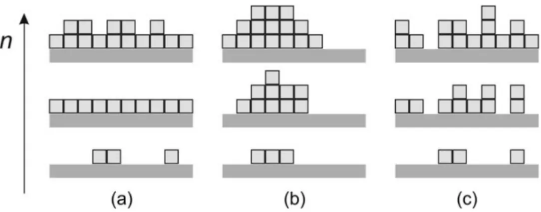
The growth mode is defined as the way of arrangement of material on the surface in a specific manner during ALD growth. Due to self-limiting nature of ALD, one might expect a rather two-dimensional-like growth for a monolayer growth per cycle. On the other hand, what is generally realized is the growth of less than a monolayer per cycle, where other growth modes can predominate, which may affect the film properties like surface roughness, density, and defectiveness.
In principle, we can classify three distinct growth modes for an ALD process. These growth modes are given as Volmer-Weber growth (island growth) [22, 23], two-dimensional growth (Frank-van der Merwe growth, layer-by-layer growth) [24], and random deposition [25]. In island growth, the new units of material are
Figure 2.3: The chemisorption mechanisms possible in ALD: (a) ligand exchange reaction of the MLn reactant with surface ”-a” groups, releasing gaseous aL, (b) dissociation of the MLn in surface M-Z sites, and (c) association of the MLn complex onto the surface. In this scheme, n=3. (Reprinted from ref [9] with the permission AIP Publishing)
chemisorbed preferentially on top of the grown material instead of starting surface due to the fact that the reactivity towards the surface of growing film is higher than the reactivity towards substrate. Most of the ALD processes follow this class of growth model. In layer-by-layer growth mode, precursors are preferentially settled in the lowest unfilled material layer covering all available sites. In this growth mode, the material grows primarily monolayer by monolayer. The last growth mode is the mix of the first two. It is a statistical growth mode, in which the material deposits with an equal probability on top of all surface sites in an ALD cycle. Figure 2.4. compares schematically layer-by-layer growth, island growth, and random deposition.
Figure 2.4: Simplified schemes of the different growth modes in ALD with in-creasing number of reaction cycles n: (a) layer-by-layer growth, (b) island growth and, (c) random deposition. (Reprinted from ref [9] with the permission AIP Publishing)
2.1.3
Choice of Precursors
As ALD depends heavily on surface chemistry, particularly the selection of proper precursor molecules with suitable ligand chemistry is highly critical for a success-ful ALD growth. To date, a large variety of materials including oxides, nitrides, sulfides, and metals have been reported with successful ALD processes. Precur-sors to be used in ALD growth process should satisfy certain requirements [7].
• Adequate Volatility: The precursor should be sufficiently volatile either at room temperature or at higher temperatures. Volatility is necessary for efficient transportation of the precursors to the ALD chamber in gas phase. Since the required precursor vapor pressure is reactor specific, it may rely on several factors, i.e. source container geometry, flow rate, substrate area, etc. Yet, in general, vapor pressure of ∼ 0.1 Torr is suitable and enables efficient material transportation in gas phase to the substrate surface. If available, liquid or gaseous precursors should be preferred, but solid precursors with reasonably high vapor pressure can be used as well in ALD processes. • Stability: The selected precursor should be thermally stable to maintain the
self-limiting growth mechanism and not decompose neither during storage, at the vaporization temperature nor during ALD processing temperature
which might lead to undesired CVD-like growth. Thermal decomposition of precursor molecules might possibly deteriorate the self-limiting film growth characteristic.
• Reactivity: The precursor should be very reactive towards the chemisorbed species to ensure rapid and complete surface saturation. Preferably, they should react with the available sites on the surface of the substrate fast and aggressively which will contribute not only in terms of shorter cycle times but also the purity of the film, high productivity, and effective precursor utilization.
• Unreactive By-products: The chosen precursor should preferably generate unreactive volatile by-products which can be removed easily from the actor. The by-products formed should be sufficiently volatile for easy re-moval to avoid corrosion problem in the reactor or in the exhaust which may shorten the lifetime of the deposition system. In addition, if the by-products are reactive, they might etch the growing film and/or substrate material.
Besides above-mentioned requirements, purity, cost effectiveness, non-toxicity, en-vironmental friendliness, easy handling and synthesis are the other requirements that a precursor should ideally fulfill.
2.1.4
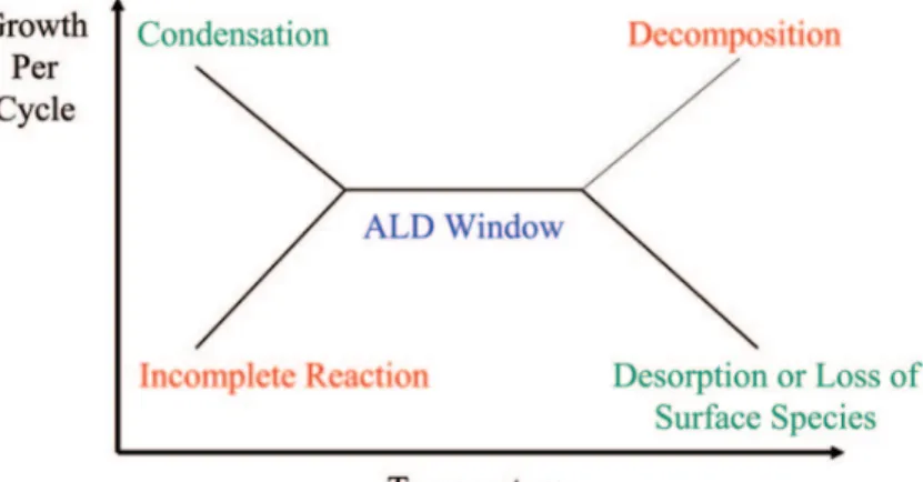
ALD Window
The processing temperature range in which self-limiting growth takes place is called as the ”ALD window”. Growth per cycle within this temperature range has an ideal constant value. Center line in Figure 2.5 presents the ALD window on the growth per cycle vs. substrate temperature graph. Outside of the ALD temperature window film deposition becomes non-ideal which results in non-self-limiting growth behavior. According to the graph, at growth temperatures below the ALD window, the precursor molecules may condense on the substrate surface
Figure 2.5: Conceptual illustration of an ALD process temperature window with respect to the substrate processing temperature.
or the surface reactions might not possess enough thermal energy to attain com-pletion. High deposition rate is observed due to the condensation of precursor molecules in this regime. On the other hand, at higher temperatures, the sur-face species could thermally decompose and cause CVD-like growth mechanism where growth-per-cycle (GPC) increases with temperature due to the additional reactant adsorption. Additionaly, growth rate may go down as well at higher temperatures because of the desorption of surface species from the surface and be unavailable for additional surface reactions.
As a result, in order to achieve appropriate chemisorption of the reactants chemically onto the surface, the temperature should be lower than the precur-sor decomposition temperature to provide lasting chemiprecur-sorption. On the other side, the temperature should be higher than the lower limit to impede precursor condensation or incomplete reaction.
2.1.5
Atomic Layer Deposition of Metal Oxides
A vast number of ALD processes has been developed for the growth of various solid inorganic materials, such as oxides, nitrides, sulfides, and metals. From these different types of inorganic materials grown, oxides have been the type most often examined.
2.1.5.1 Titanium Dioxide, TiO2
TiO2 is one of the first oxides grown by ALD. Atomic layer deposition of TiO2
films have been achieved by various ALD processes using halide, alkoxide, alky-lamide, and heteroleptic precursors as the metal source within a temperature range of 100 − 600◦C [26–31].
TiO2 has been extensively studied due to its wide practical features, such
as high catalytic activity, chemical and physical stability. It mostly finds ap-plications in the field of chemical sensors, microelectronics, medical and optical applcations. The most common polymorphs of TiO2 are rutile and anatase. The
band gaps of rutile and anatase phases are 3.0 eV and 3.2 eV, respectively.
In earlier works, the most popular precursors combination employed for ALD TiO2 was TiCl4 with H2O. TiCl4 has been a typical precursor for TiO2 due to its
good volatility, reactivity with water, cost effectiveness, and stability.The reac-tion between these two precursors can be generalized by the following simplified reaction equation:
T iCl4(g) + 2H2O(g) → T iO2(s) + 4HCl(g) (2.4)
k − (OH)x+ T iCl4(g) → k − Ox− T i − Cly + HCl(g) (2.5)
k − Ox− T i − Cly + H2O → k − Ox− T i − (OH)y + HCl(g) (2.6)
The above half cycle reactions were introduced by Aleskovski and Kol’tsov in 1965 and 1969, separately [11, 32]. A Ti-O Lewis acid-base complex is formed during each half-reaction and HCl is generated as the reaction by-product.
2.1.5.2 Zinc Oxide, ZnO
ZnO is a direct wide band gap semiconductor with a band gap of 3.37 eV and close to that of TiO2. Despite having a large band gap, it shows low resistivity.
Actually, the characteristics of TiO2 and ZnO are somewhat alike in terms of
application areas. Like TiO2, ZnO can be used in optical, electrical, and sensing
applications. In the nature, ZnO can be found in three crystalline forms: cubic zincblende, rocksalt, and hexagonal wurtzite, the last being the most stable in ambient conditions. ZnO deposition has been extensively investigated by many studies [33–38]. Because of their high reactivity, diethyl zinc (DEZ) and H2O
have been the most prevalently exploited precursors for ZnO-ALD. The reaction between these two precursors can be described by the following reaction equation:
Zn(CH2CH3)2(g) + H2O(g) → ZnO(s) + 2CH3CH3(g) (2.7)
k − OH + Zn(CH2CH3)2(g) → k − O − Zn − CH2CH3+ CH3CH3(g) (2.8)
k − O − Zn − CH2CH3+ H2O(g) → k − O − Zn − OH + CH3CH3(g) (2.9)
A Zn-O Lewis acid-base complex is formed during each half-reaction, and ethane is produced as a reaction by-product.
2.1.5.3 Aluminum Oxide, Al2O3
Al2O3 is probably the most widely investigated ALD material for many diverse
applications. Its favorable properties such as high band gap, thermal stability, proper dielectric constant make Al2O3a very attractive material of choice [39–44].
The most widely studied aluminium precursor is trimethylaluminium (TMA). The deposition process of TMA/H2O can be regarded as a representative process
which depicts ALD in general. An Al-O Lewis acid-base complex is formed dur-ing each half-reaction, and methane is formed as a by-product. The simplified reaction can be described with the following reaction equation:
2(Al(CH3)3)(g) + 3H2O(g) → Al2O3(s) + 6H2O(g) (2.10)
k − OH + (Al(CH3)3)(g) → k − O − Al − (CH3)x+ CH4(g) (2.11)
2.2
Self-Assembled Peptide Nanostructures
2.2.1
Peptide Chemistry
Amino acids are the basic units of peptide sequences. They are organic com-pounds containing functional amine (-NH2) and carboxylic acid (-COOH) groups,
along with side chain which is specific to each amino acid. There are 20 different kinds of amino acids most commonly occurring in nature. They can be classified based on their capacity for interaction with water: polar, non-polar, acidic, and basic. They may also be categorized according to their side chain group type: aliphatic, acyclic, and aromatic.
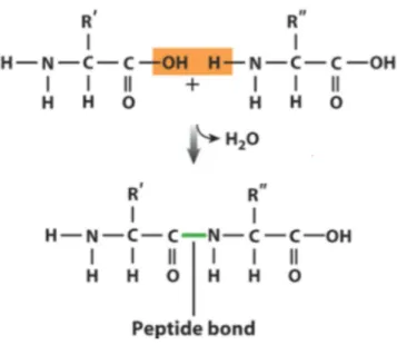
Peptide is a compound that contains two or more amino acid monomers linked together by peptide bonds, aka amide bond (Figure 2.6). It is a dehydration reaction where a water molecule is removed. The shortest peptides are dipeptides, in which two amino acids are covalently linked. Polypeptides are long, continuous, and well-defined large structures. The covalent bond is formed between two amino acids when the carboxyl group (C-terminus) of one amino acid reacts with amine group (N-terminus) of another. Except cyclic peptides, all peptides possess C-terminal and N-C-terminal residue at the end of the peptide. Conventionally, the amino acid residue with N-terminal residue is written to the left and carboxyl group on the C-terminal residue is placed on the right. Names of peptides begin from their N-terminal residue.
2.2.2
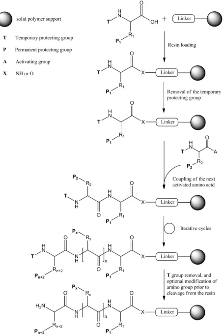
Solid Phase Peptide Synthesis
Solid phase peptide synthesis (SPPS) is an extensively used method to synthesize long amino acid sequences with high yield. It is an alternative method to solution phase peptide synthesis which suffers from purity, low solubility of the growing peptides, and high-yield. The method is pioneered by Robert Bruce Merrifield who was awarded Nobel Prize in chemistry in 1984 for his study published in 1963 [45]. With this neat approach, Merrifield achieved the synthesis of tetrapeptide
Figure 2.6: Condensation of two amino acids to form a dipeptide through a peptide bond
chain using polystyrene resin as a solid matrix, which plays an important role in the success of SPPS. The grown peptide is covalently tethered at one end to the functionalized solid support which enables for simple stepwise syntheses and prevents a large number of individual steps. Besides, it shortens the time required and allows the synthesis of previously unapproachable peptides. It is a step-by-step growth of peptide on an insoluble solid resin in consequence of repetitive amino acid couplings [46].
In principle, it is a stepwise addition of the N-protected C-terminus amino acids to the hydroxyl (or chloro) or amino resin. There are four essential cycles for each step which follow as deprotection-washing-coupling-washing. The pro-tecting group of the first amino acid is deprotected, revealing a new N-terminal amine to which an additional amino acid might be coupled. While the amino acids elongates on the solid resin, excess of coupling reagents, unreacted amino acids and by-products remain in the solvent. Upon completion of short peptide sequence, the peptide chain is cleaved from solid resin with the help of an an-hydrous acid reagent. Due to the nature of iterative stepwise cycles, elongation of amino acids on the solid support can be ultimately controlled. There are two strategies majorly used to protect N-termini of amino acid monomers: Fmoc
and Boc. At the beginning, the first Fmoc amino acid is bound to a solid resin, which acts as support in growth of peptide. After attachment of first N-protected amino acid, the deprotection of Fmoc is accomplished by introducing a base to the medium, usually piperidine. In SPPS, insoluble polystyrene resins are mostly exploited for immobilized peptide growth on the solid phase. Wang resins and Rink amide resins are the most preferable ones among other resins. Figure 2.7 presents the principles of SPPS process [47].
2.2.3
Self-Assembly of Peptides
Self-assembly is a natural, bottom-up process that organizes building blocks into well-ordered nanostructures in a spontaneous manner. It is an attractive route for production of novel multi-functional materials in relatively mild conditions [48–51]. Inspired by the protein assembly in biological systems, several peptides that self-assemble to form various nanostructures such as nanofibers, nanotubes, nanovesicles, nanoribbons, and fibrous scaffolds, have been intensely studied by many researchers. These self-assembled peptides find many applications in tissue engineering, drug delivery, food science, cosmetic industry, and nanotechnology, particularly molecular electronics.
An excellent advantage of harnessing self-assembled peptides to create nano-materials in a bottom-up approach is that unique features can be combined; the peptides can be modified or functionalized. Self-integration of small, simple build-ing blocks allows one to form precisely defined nanostructures. Self-assembly of peptide is primarily governed by weak non-covalent interactions such as electro-static interactions, coordination binding, hydrogen bonding, - interactions, solvo-phobic effects, and Van der Waals interactions [52,53]. These types of interactions are powerful driving forces to self-assembly and also contribute stabilization of the secondary structure of peptides and proteins [54].
Table 2.1: List of non-covalent interactions
Type of Interaction Strength (kJ/mol) Range Properties Electrostatic 50-300 long Non-selective Coordination binding 50-200 short Directional
Hydrogen bonding 5-120 short Selective, directional π-π interaction 0-50 short Directional
Solvophobic Depends on solvent type short Directional constraint Van der Waals <5 short Non-directional, non-selective Covalent (reference) 350 short Irreversible
2.2.3.1 Electrostatic Interactions
This type of interaction stands for Coulomb interactions between electrically charged species. Electrostatic interactions are important in the formation of qua-ternary structure of protein and its functionality. Short peptides can be brought together via electrostatic interaction to trigger assembly process. This interaction type has been widely studied in assembly processes by researchers in an attempt to fold peptides into certain morphologies.
2.2.3.2 Coordination Interactions
Metal-ion coordination can be harnessed to direct peptide assembly. In this kind of interactions, side chains serve as ligands and the metal-ion interactions with the side chains are designed to constrain the geometry. This interaction plays an important role to induce secondary or tertiary structure formation in short peptides in an effort to form artificial metalloenzymes and to direct the assembly of peptides for active binding sites of biological targets. There are numerous reports showing that multiple metal-ions can be selectively introduced into trimeric or tetrameric scaffolds assembly.
2.2.3.3 Hydrogen Bonding
Hydrogen bonding is one of the most abundant interaction mode in peptides and proteins. It is an inherent interaction and plays a vital role in folding and supramolecular assembly of proteins. β-sheet and α-helix motifs occur in struc-tural organization of assembly process. β-sheet is formed due to hydrogen bond-ing interactions between the backbone amide and carbonyl. The direction of the strands determines whether the sheet is parallel or anti-parallel. All peptide-based assembling materials somehow involve hydrogen bonding interactions. Unlike the β-sheets, the formation of individual peptide chains in which backbone amide parts are intra-molecularly hydrogen bonded results in the α-helices structures.
Occasionally, the so-called coiled coils can be formed by coiling and assembling of single α- helices.
2.2.3.4 π-π Interactions
π-π interactions are a kind of non-covalent interaction that involves π systems. The electron-rich π systems can stabilize overall assembly architecture. The inter-action is most likely to occur between aromatic ring structures in which aromatic π-systems can overlap each other to stabilize assembling structure. The most common types of π-interactions involve metal- π interactions, polar- π interac-tions, aromatic-aromatic interacinterac-tions, and π donor-acceptor interactions. The interaction is pivotal in nucleobase stacking in DNA and RNA molecules, protein folding, and protein-ligand recognition.
2.2.3.5 Solvophobic Interactions
Particularly, solvophobic interactions are crucial in biological systems. Solvo-phobic aggregation phenomena is prevalent for amphiphilic molecules where the solvophobic parts of the molecules are prone to aggregate to minimize their sur-face area in contact with solvent, whilst the solvophilic parts strive to remain solvated. In principle, solvophobic aggregation occurs because of favorable en-tropy rather than enthalpy. It is considered to be accomplished in two stages which are solvation and solvophobic escape from the solvent; in the former stage solvent molecules are released, and as a result total entropy is increased.
2.2.3.6 Van der Waals Interactions
This interaction is based on attractive or repulsive forces between molecules or atomic groups. They are relatively weak compared to covalent bonds, but play an essential role in protein folding. There are three kinds of Van der Waals forces including Keesom force; an interaction between permanent dipoles, Debye force;
an interaction between a permanent dipole and induced dipole, London dispersion force; an interaction between instantaneously induced dipoles. A very well-known example of cumulative impact of van der Waals forces is adhesion mechanism of geckos to different surfaces. Once aliphatic and aromatic peptide amphiphiles assemble into ordered nanostructures, they are also stabilized via Van der Waals forces.
2.2.4
Self-Assembly of Peptide Amphiphiles
Peptide amphiphiles (PAs) are comprised of oligo-peptides that possess both hy-drophobic alkyl tail and hydrophilic ends, resembling to lipids. Depending upon the the distribution and the number of amino acids in the peptide sequence, var-ious structures, including nanofibers, nanotape, nanorod, nanovesicle, nanotube, and micelle can be formed. The PA molecules have the tendency to self-assemble via β-sheet secondary structures which give rise to the formation of 1D pep-tide nanostructures through intermolecular hydrogen bonding [1], schematically shown in Figure 2.8. Interactions between 1D peptide nanostructures further
Figure 2.8: Self-assembly of PA molecules into a cylindrical micelle. From ref [1]. Reprinted with permission from AAAS.
entangle into 3D peptide networks. The driving force for the formation of 1D nanostructures by PAs in water results from the combination of at least three main energy contributions: hydrophobic interaction between the alkyl tails; hy-drogen bonding of the peptides, and electrostatic repulsions between the charged amino acids. The first two forces are attractive ones which are inclined to help the aggregation of PA molecules, whilst electrostatic repulsions leads to disasso-ciation of PA molecules. The rigidity of the peptide nanostructures can be tuned by the addition of a phospholipid that can only interact via the alkyl tail and not hydrogen bond to the peptide segment of the PA molecule.
Chapter 3
Experimental Details
3.1
Materials and Reagents
Fmoc- and Boc- protected amino acids, Rink Amide MBHA resin, and HBTU were purchased from NovaBiochem and ABCR. The other chemicals were pur-chased from Fisher, Merck, Alfa Aesar, or Aldrich and used as received. The 2.2 mm thick fluorine doped tin oxide (FTO) coated glass (sheet resistivity of 7 Ω/sq), Ruthenizer 535-bis TBA (N719) photosensitizer dye, Iodolyte AN 50 electrolyte, and Meltonix 1170-60 thermoplastic were purchased from Solaronix.
3.2
Peptide Synthesis and Characterization
Peptide molecules, as shown in Figure 3.1, were synthesized by solid phase pep-tide synthesis method. Peppep-tide sequence was constructed on Rink Amide MBHA resin (0.59 mmole/g). 0.5 mmole peptide synthesis was carried out; 2 equiva-lents (with respect to resin) of amino acids and lauric acid were used in each coupling. Amino acids or lauric acid (2 eq.) were activated with DIPEA (3 eq.) and HBTU (1.98 eq) prior to coupling. All couplings were carried out in
dimethylformamide (DMF). At the end of the coupling cycles, resin was cleaved from the resin by concentrated trifluoroacetic acid (TFA). For this purpose, a 10 mL cleavage cocktail (TFA:TIS:H2O = 9.5:0.25:0.25) was prepared; Milli-Q
water (H2O) and triisopropylsilane (TIS) were used as scavengers. Cleaved
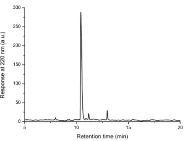
pep-tide was collected by dichloromethane (DCM), which was later removed alongside with TFA by rotary evaporation. Residual material was triturated by cold di-ethyl ether. White peptide precipitate was completely separated from ether by centrifugation; the centrifugate was dissolved in water, deep freezed at −80◦C and finally lyophilized. Lyophilized peptide was characterized by high resolu-tion time-of-flight mass spectrometer coupled to liquid chromatography system (Agilent 1200/6210), as shown in Figures 3.2 and 3.3.
Figure 3.1: Structural formula of lauryl-VVAGK-Am peptide amphiphile
Figure 3.3: Mass spectrum of the lauryl-VVAGK-Am peptide amphiphile. Calcu-lated m/z is 653.4840 (M), found m/z is 654.4798 (M+H) and 1307.9487 (2M+H).
3.3
Photoanode Fabrication and
Characteriza-tion
First, fluorine doped tin oxide (FTO) glass (1.67cm x 1.67cm) was treated with 100 mL of H2O:NH4OH:H2O2 (5:1:1) solution at 75◦C for 30 minutes. Then, 4
µL of 2% (wt/v) peptide amphiphile solution was spread directly on FTO with restricted area of 0.09π cm2 ( 0.28 cm2), afterwards peptide solution was gelled
by NH3 vapor in closed container. Obtained hydrogel was converted to alcogel by
series of gradual alcohol in water mixtures (15%, 30%, 45%, 60%, 75%, 90% and 100%); finally, alcogel was converted to aerogel by critical point drying just be-fore ALD process. FEI Quanta 200 FEG scanning electron microscope with EDX attachment was used to study morphology and chemical composition of TiO2 and
ZnO nanonetworks. Peptide aerogel was sputter coated with 6 nm of Pt prior to SEM imaging. FEI Tecnai G2 F30 transmission electron microscope was used to obtain TEM micrographs. PANalytical X’Pert Powder X-ray Diffractometer was used to analyze crystal structures of TiO2 and ZnO nanonetworks. Cary 5000
UV-Vis-NIR spectrophotometer with an internal diffuse reflectance attachment was used to record diffuse reflectance spectra of TiO2 and ZnO. WITec Alpha
300S Scanning Near-field Optical Microscope with Raman module was used to characterize the samples. Calcined TiO2 and as-synthesized ZnO samples were
immersed into 0.3 mM N719 dye solution in acetonitrile tert-butoxide and incu-bated for at least 24 h.
3.4
Atomic Layer Deposition of TiO
2and ZnO
ALD was employed to deposit TiO2 or ZnO in a commercial thermal ALD reactor
(Ultratech/CambridgeNanotech Inc. Savannah S100). The substrate tempera-ture was kept at 150◦C during the ALD process using Ti(NMe2)4, Zn(Et)2, and
H2O as titanium, zinc, and oxygen precursors, respectively. Prior to deposition,
Ti(NMe2)4 precursor was preheated to 75◦C. As carrier gas, N2 was employed
with a flow rate of 20 sccm. The deposition was carried out using successive 3 different numbers of deposition cycles including 100, 150, and 200 cycles of TiO2,
and 100, 125 and 150 cycles of ZnO. As-synthesized TiO2 samples were calcined
in accordance with the following procedure: ramp from 25◦C to 150◦C with 5◦C/min, 150◦C to 350◦C with 1◦C/min, from 350◦C to 450◦C with 5◦C/min and wait for 30 min.
3.5
Solar Cell Assembly and Characterization
On the top of the photoanode 25 nm Pt-coated glass (cathode) was placed, ther-moplastic was used as a spacer between two electrodes, and I−/I3−electrolyte was sandwiched between two electrodes. Photovoltaic current-voltage (I-V) measure-ments of the solar cells were recorded from the circular active area of 0.09π cm2 ( 0.28 cm2). A Newport full-spectrum solar simulator with Air Mass (AM) 1.5G
filter from Oriel was used as the light source in I-V measurements. Simulator was operated at the following parameters: AM 1.5G, 100 mW/cm2 and 25◦C. Solar
3.6
ICP-MS Measurements
Thermo X series II inductively coupled plasma-mass spectrometer (ICP-MS) was used to analyze metal ion concentrations. N719 dye was desorbed from TiO2
and ZnO surfaces by dilute aqueous ammonia; desorbed dye was then digested in 4 mL of aqua regia (HNO3:HCl=1:3). Prior to ICP-MS analysis, samples were
diluted by 2% aqueous HCl. Adsorbed N719 amounts were back calculated based on ruthenium concentration. TiO2 was dissolved in 5 mL mixture of conc. HNO3
and HF (4:1), and ZnO was dissolved in 1 mL of conc. HNO3. Prior to analysis,
samples were diluted by 2% aqueous HNO3. Deposited metal oxide amounts were
Chapter 4
Results and Discussion
A three-dimensional nanofibrous template formed by self-assembling peptide am-phiphile molecules was used in deposition of TiO2 and ZnO with varying
thick-ness. As a proof of a principle, deposited TiO2 and ZnO were utilized in
dye-sensitized solar cell (DSSC) fabrication and effect of metal oxide layer thickness on cell parameters was studied. For this purpose, the self-assembled peptide amphiphile with the sequence lauryl-VVAGK-Am was synthesized (Figure 4.1a). The PA molecules self-assemble into nanofiber network under basic conditions. Self-assembly of the peptide amphiphile in water leads to hydrogel formation; hy-drogel is composed of three-dimensional PA nanofiber network entrapping the sol-vent (Figure 4.1b). Removal of the solsol-vent with minimal damage to PA nanonet-work enables one to obtain highly porous organic template (Figure 4.1c).
Transformation of hydrogel to aerogel is achieved by critical point drying tech-nique. Obtained aerogel was used as a template and coated with TiO2 and ZnO
of different thickness. After calcination, hybrid 100, 150 and 200-cycle TiO2
ma-terials result in nanotube networks (Figures 4.2 a-c and 4.3 a-c) with 5.18±0.26, 7.52±0.24 and 10.25±0.49 nm wall thickness, respectively.
Figure 4.1: Fabrication of nanostructured peptide template. a) lauryl-VVAGK-Am peptide, b) schematic hydrogel, and c) peptide aerogel
Figure 4.2: SEM micrographs of a) 100-cycle, b) 150-cycle, and c) 200-cycle TiO2
nanonetworks after calcination.
Energy dispersive X-ray (EDX) spectroscopy verified TiO2 and ZnO coatings
based on presence of Ti or Zn and O atoms; C and N atoms pertaining to organic template were also registered (Figures 4.4 and 4.5). Calcination process removes the organic template and transforms amorphous titania to its anatase form. In order to verify phase transformation, XRD and Raman spectra were recorded. Before calcination, XRD and Raman spectra of as-synthesized TiO2 materials
show that material is highly amorphous with negligible presence of rutile phase (Figures 4.6 and 4.7) [55].
Figure 4.3: TEM micrographs a) 100-cycle, b) 150-cycle, and c) 200-cycle TiO2
coated nanofibers after calcination. Scale bar is 50 nm.
After calcination, XRD and Raman spectra (Figure 4.8 and 4.9) confirmed that titania transformed successfully to its anatase form. Alongside with anatase form, some presence of brookite titania was detected as well. An extra peak (121) at 2θ = 30◦C in XRD spectra and several extra peaks at 246 cm−1, 323 cm−1 and 365 cm−1 in Raman spectra of calcined TiO2 materials indicate presence of
brookite form [56, 57].
ZnO coatings achieved on peptide nanonetwork template did not require fur-ther calcination. Calcination was not performed for ZnO materials, which were already crystalline with shell thickness of 17.48±1.10 nm, 20.96±0.89 nm and 23.39±1.32 nm for 100, 125, and 150 deposition cycles, respectively (Figures 4.10 a-c and 4.11 a-c).
Based on XRD and Raman spectroscopy results (Figures 4.12 and 4.13), crys-talline ZnO coatings exhibited hexagonal wurtzite crystal phase. Raman spectra of ZnO materials, in addition to standard peaks [58], includes a peak at 268 cm−1, which was assigned to nitrogen-related mode (NRM). This mode is thought to arise due to disorder or defects favored in the presence of N [59]. NRM in synthe-sized ZnO materials can stem from peptide-ZnO interface; PAs upon assembly into nanofibers are expected to expose amine groups of lysine residues onto the surface.
ZnO in its wurtzite form is a wide bandgap semiconductor and is utile for photoanode construction. Morphology of obtained nanostructured TiO2and ZnO
photoanodes was uniform and template effect was preserved throughout the whole anode thickness (Figure 4.14).
For ultra-thin films, layer thickness is expected to have an impact on effective material bandgap. To estimate bandgaps (Eg) of nanostructured semiconductor
TiO2 and ZnO materials, diffuse reflectance spectra were recorded. Using the
Kubelka-Munk function (eq. 4.1) diffuse reflectance data were transformed into Tauc plots, (hνF(R))1/n versus hν, with an assumption of direct allowed electron transfer (n= 0.5) [60]. R in the equation stands for an absolute reflectance.
F (R) = (1 − R)
2
2R (4.1)
As-synthesized TiO2 samples exhibited estimated bandgap values of 3.41, 3.31,
and 3.28 eV for 100, 150, and 200 deposition cycles, respectively (Figure 4.15). As expected for nanomaterials, Eg increases as material becomes thinner (Eg100
Eg150 > Eg200). Thinner material imposes greater quantum confinement on
electron transfer, hence bandgap widening is observed. Surprisingly, calcination led to reversal of order of estimated Eg values (Eg100 Eg150 < Eg200); the new
values are 2.80, 3.21, and 3.23 eV for 100, 150, and 200 cycles, respectively (Figure 4.16).
Based on the presence of residual carbon in EDX spectra (Figure 4.17) of the calcined samples, it can be speculated that thermally decomposing organic tem-plate introduces impurities into the material; and therefore, the thinnest material (100-cycle TiO2) is the most affected one.
Lee et al. in silico studied the electronic properties of C- and N-doped titania [61]. Based on first principles density functional calculations, it was proposed that the red shift in optical absorption of doped material is caused by the presence of isolated C 2p states in the band gap of TiO2 rather than by a band gap
narrowing. Interaction between C impurity atoms and neighbouring Ti atoms due to coupling of the top most C 2p state with Ti 4d state is relatively stronger than in N-doped TiO . Xu et al. also reported similar results, band structural
studies revealed that the visible light activity is related to the isolated impurity states in the band gap [62].
In the case of ZnO, estimated band gaps were 3.27 eV, 3.18 eV, and 3.24 eV for 100, 125 and 150 cycle ZnO materials, respectively (Figure 4.18). It is clear that estimated band gaps of relatively thick conformal ZnO layers did not show a linear dependence on cycle number, hence material thickness.
Current density vs. voltage (J-V) curves of devices constructed from obtained materials demonstrate that material thickness has its impact on device parame-ters. 100-cycle titania sample demonstrated superior Voc compared to 150- and 200-cycle titania (Voc100 Voc150 > Voc200) (Figure 4.19).
Despite this fact, Jsc was inferior for 100-cycle titania. Table 4.3 summarizes
J-V parameters for fabricated TiO2-based DSSC devices. It is clear that device
with 150 cycles of TiO2 deposition is optimal as it is close to 200-cycle device in
terms of efficiency, although it possesses less deposited material. The efficiency of 100-cycle device is inferior to 150- and 200-cycle devices, which perform about 2 times better.
Thicker titania nanostructures owing to their higher surface area can accom-modate higher number of sensitizer molecules. ICP-MS analysis has shown that adsorbed sensitizer molecule amounts were as 5.89 µg, 9.40 µg, and 13.75 µg for 100, 150, and 200 cycles, respectively; deposited TiO2 was also cycle-dependent
Table 4.1: N719 sensitizer amounts adsorbed by TiO2
TiO2 cycles 101 Ru (ng) N719 (µg) 47 Ti (ng) TiO2 (µg)
100 501.5 5.89 61260 102.21
150 799.5 9.40 102300 170.68
200 1169 13.75 117600 196.22
Devices fabricated from nanostructured ZnO have shown similar performance in terms of efficiency (Figure 4.20); close Vocand Jsc values were observed. Based
on ICP-MS results, adsorbed sensitizer amounts were also similar, 391.36 µg, 403.47µg, and 399.30 µg for 100, 125, and 150 cycles of ZnO deposition, respec-tively; on contrary deposited ZnO was cycle-dependent and close to 1 mg (Figure 4.21, 4.23 and Table 4.2).
Table 4.2: N719 sensitizer amounts adsorbed by ZnO
ZnO cycles 101 Ru (ng) N719 (µg) 66 Zn (ng) ZnO (µg) 100 33280 391.3619 576400 717.46 125 34310 403.4743 770800 959.43 150 33955 399.2996 938400 1168.05
The main difference for ZnO devices was in fill factor values; a 100-cycle ZnO device had the highest fill factor, which actually provided higher efficiency for the device. Based on material-efficiency ratio, 100-cycle device is an optimal one among ZnO devices.
Moreover, TiO2 nanonetworks surpassed ZnO nanonetworks in terms of
struc-tural integrity, because ZnO nanonetworks with the same material thicknesses (33, 50, 67 cycles) could not be utilized in functional devices due to disintegra-tion of the networks in I−/I3− electrolyte; therefore, thicker ZnO nanostructures were deposited. Nevertheless, ZnO nanonetworks demonstrated superior dye ad-sorption properties, which can be utilized in TiO2-ZnO core shell nanostructured
Devices based on TiO2 and ZnO nanonetworks have demonstrated
compet-ing efficiencies, although TiO2 nanonetworks had higher dependence on material
thickness. Taking into account amounts of deposited metal oxide and adsorbed dye, TiO2 based devices outperform ZnO based ones (Table 4.3).
Table 4.3: Cell parameters of nanostructured TiO2 and ZnO devices
Material
V
oc(V)
J
sc(mA/cm
2)
FF
η
100-cycle TiO
20.755
1.026
0.60
0.47
150-cycle TiO
20.720
2.413
0.56
0.97
200-cycle TiO
20.713
2.162
0.65
1.00
100-cycle ZnO
0.610
3.098
0.53
1.01
125-cycle ZnO
0.620
3.284
0.47
0.96
150-cycle ZnO
0.630
3.213
0.44
0.90
Figure 4.6: XRD spectra of as-synthesized 100-, 150- and 200-cycle TiO2
Figure 4.8: XRD spectra of 100, 150, and 200-cycle TiO2
Figure 4.9: Raman spectra of 100, 150, and 200-cycle TiO2. A = anatase, B =
Figure 4.10: SEM micrographs of a) 100-cycle, b) 125-cycle, and c) 150-cycle ZnO nanonetworks
Figure 4.11: TEM micrographs a) 100-cycle, b) 125-cycle, and c) 150-cycle ZnO coated nanofibers. Scale bar is 50 nm.
Figure 4.12: XRD spectra of 100, 125, and 150-cycle ZnO
Figure 4.14: Cross-sectional view of nanostructured TiO2 and ZnO photoanodes.
a-c) 100-, 150- and 200-cycle TiO2, d-f) 100-, 125- and 150-cycle ZnO.
Figure 4.18: Tauc plots of ZnO
Figure 4.20: J-V curves of 100, 125 and 150-cycle ZnO devices
Figure 4.21: Ru calibration line
Chapter 5
Conclusion
Self-assembled peptide amphiphile nanonetwork was successfully used as a tem-plate for fabrication of nanostructured TiO2 and ZnO materials. The template
was coated with TiO2 and ZnO of varying thickness by atomic layer
deposi-tion technique. For TiO2 based devices, we observed that material thickness has
prominent effects on device parameters and overall performance. The thinnest material (100 cycles) has demonstrated enhanced Voc, although generated
pho-tocurrent was inferior to those of thicker materials.
Material thickness affects effective band gap of final metal-oxide layers, which correlates with observed Vocvalues. Thicker nanostructures (150 and 200 cycles)
with higher TiO2 content adsorbed greater amounts of sensitizer molecules, which
resulted in higher photocurrents. Among thicker material devices, 150-cycle de-vice is the optimal one, as it possesses similar efficiency to 200-cycle dede-vice with less deposited titania and less adsorbed sensitizer.
Devices fabricated from nanostructured ZnO have shown similar performance in terms of efficiency. Efficiencies were similar and slightly decreased with in-creasing cycle number. Devices demonstrated close Voc and Joc values, based
on material-efficiency ratio and higher fill factor, 100-cycle ZnO device exhibited optimal device performance.
Substantially higher dye loading observed for ZnO nanonetworks gives an op-portunity to boost efficiency of TiO2 based devices in TiO2-ZnO core-shell design
with just a few ZnO deposition cycles.
In conclusion, template assisted synthesis strategy is a unique tool to construct materials in which physical dimensions can be precisely tailored. Conformal du-plication of the morphologies by using self-assembled peptide templates and ALD pave the way for the formation of sophisticated functional nanostructures.
To the best of our knowledge, this is the first report demonstrating fabrication of anodic materials on self-assembled peptide amphiphile template by ALD. We hope this work will be an inspiring example for biomimetic materials and ma-terials chemistry fields. As mentioned in previous sections, ALD is an effective tool to functionalize and form porous structures with high surface area. Thus, over the last decades, scientists in DSSC community have shown the immense in-terest and actively exploited ALD technique. We anticipate that such proposals and developments in fabrication of novel nanomaterials will enhance the device properties and will have enormous promise in all other innovative devices.
Further, core-shell structures can be fabricated by coating this one dimensional nanostructures. As a future study, we plan to deposit ZnO on top of the TiO2
surface and vice versa structure with ALD, facilitating precise tuning of the elec-tronic, optical, and chemical properties in order to optimize their interfaces. By doing this, we expect an increase in the performance of the device parameters. Basically, the core-shell structure may reduce the electron-hole recombinations in the solar cell and increase the adsorption of sensitizer molecules which leads to a higher current density. The core-shell structures can also be used in artificial photosynthesis in an attempt to split the water molecule for H2 generation and
reduce the CO2 into more useful fuels.
Along with the core-shell structures, this highly porous nanomaterial can be utilized in light-unassisted catalytic applications as well. ALD is a unique methodology for the atomically precise design and synthesis of catalytic materi-als which can be used effectively in organic transformations, in particular. Other
than metal-oxides, metals can be grown with ALD as well. In another future direction, metal-decorated nanofibers can be exploited in catalytic applications to improve activity, selectivity, and stability issues under a variety of conditions.
![Figure 2.2: Simplified mechanism for one unit ALD reaction cycle. (Reprinted from ref [9] with the permission AIP Publishing)](https://thumb-eu.123doks.com/thumbv2/9libnet/5605871.110588/20.918.272.698.415.1042/figure-simplified-mechanism-reaction-cycle-reprinted-permission-publishing.webp)

![Figure 2.8: Self-assembly of PA molecules into a cylindrical micelle. From ref [1].](https://thumb-eu.123doks.com/thumbv2/9libnet/5605871.110588/35.918.244.732.703.1016/figure-self-assembly-pa-molecules-cylindrical-micelle-ref.webp)