Large-area semi-transparent light-sensitive
nanocrystal skins
Shahab Akhavan,1 Burak Guzelturk,1 Vijay Kumar Sharma,1 and Hilmi Volkan Demir1,2,*
1UNAM–Institute of Materials Science and Nanotechnology, Department of Electrical and Electronics Engineering,
Department of Physics, Bilkent University, Ankara, 06800, Turkey
2School of Electrical and Electronic Engineering, School of Physical and Mathematical Sciences, Nanyang
Technological University, Singapore, 639798, Singapore
Abstract: We report a large-area, semi-transparent, light-sensitive nanocrystal skin (LS-NS) platform consisting of single monolayer colloidal nanocrystals. LS-NS devices, which were fabricated over areas up to 48 cm2 using spray-coating and several cm-squares using dip-coating, are operated on the principle of photogenerated potential buildup, unlike the conventional charge collection. Implementing proof-of-concept devices using CdTe nanocrystals with ligand removal, we observed a substantial sensitivity enhancement factor of ~73%, accompanied with a 3-fold faster response time (<100 ms). With fully sealed nanocrystal monolayers, LS-NS is found to be highly stable under ambient conditions, promising for low-cost large-area UV/visible sensing in windows and facades of smart buildings.
©2012 Optical Society of America
OCIS codes: (160.4236) Nanomaterials; (220.4241) Nanostructure fabrication; (230.0230)
Optical devices; (280.4788) Optical sensing and sensors; (250.0250) Optoelectronics; (250.5590) Quantum-well, -wire and -dot devices.
References and links
1. S. V. Gaponenko, Introduction to Nanophotonics (Cambridge University Press, 2010).
2. H. V. Demir, S. Nizamoglu, T. Erdem, E. Mutlugun, N. Gaponik, and A. Eychmüller, “Quantum dot integrated LEDs using photonic and excitonic color conversion,” Nano Today 6(6), 632–647 (2011).
3. E. H. Sargent, “Colloidal quantum dot solar cells,” Nat. Photonics 6(3), 133–135 (2012).
4. G. Konstantatos and E. H. Sargent, “Nanostructured materials for photon detection,” Nat. Nanotechnol. 5(6), 391–400 (2010).
5. S. A. McDonald, G. Konstantatos, S. Zhang, P. W. Cyr, E. J. D. Klem, L. Levina, and E. H. Sargent, “Solution-processed PbS quantum dot infrared photodetectors and photovoltaics,” Nat. Mater. 4(2), 138–142 (2005). 6. H. V. Demir, S. Nizamoglu, E. Mutlugun, T. Ozel, S. Sampra, N. Gaponik, and A. Eychmüller, “Tuning shades
of white light with multi-color quantum-dot-quantum-well emitters based on onion-like CdSe-ZnS heteronanocrystals,” Nanotechnology 19(33), 335203 (2008).
7. N. Cicek, S. Nizamoglu, T. Ozel, E. Mutlugun, D. U. Karatay, V. Lesnyak, T. Otto, N. Gaponik, A. Eychmüller, and H. V. Demir, “Structural tuning of color chromaticity through nonradiative energy transfer by interspacing CdTe nanocrystal monolayers,” Appl. Phys. Lett. 94(6), 061105 (2009).
8. S. Nizamoglu, E. Mutlugun, O. Akyuz, N. K. Perkgoz, H. V. Demir, L. Liebscher, S. Sapra, N. Gaponik, and A. Eychmüller, “White emitting CdS quantum dot nanoluminophores hybridized on near-ultraviolet LEDs for high-quality white light generation and tuning,” New J. Phys. 10(2), 023026 (2008).
9. E. Mutlugun, I. M. Soganci, and H. V. Demir, “Nanocrystal hybridized scintillators for enhanced detection and imaging on Si platforms in UV,” Opt. Express 15(3), 1128–1134 (2007).
10. C. B. Murray, D. J. Noms, and M. G. Bawendi, “Synthesis and characterization of nearly monodisperse CdE (E = sulfur, selenium, tellurium) semiconductor nanocrystallites,” J. Am. Chem. Soc. 115(19), 8706–8715 (1993). 11. J. M. Luther, M. Law, M. C. Beard, Q. Song, M. O. Reese, R. J. Ellingson, and A. J. Nozik, “Schottky solar cells
based on colloidal nanocrystal films,” Nano Lett. 8(10), 3488–3492 (2008).
12. J. Zhao, J. A. Bardecker, A. M. Munro, M. S. Liu, Y. Niu, I.-K. Ding, J. Luo, B. Chen, A. K.-Y. Jen, and D. S. Ginger, “Efficient CdSe/CdS quantum dot light-emitting diodes using a thermally polymerized hole transport layer,” Nano Lett. 6(3), 463–467 (2006).
13. S. H. Im, Y. H. Lee, S. I. Seok, S. W. Kim, and S.-W. Kim, “Quantum-dot-sensitized solar cells fabricated by the combined process of the direct attachment of colloidal CdSe quantum dots having a ZnS glue layer and spray pyrolysis deposition,” Langmuir 26(23), 18576–18580 (2010).
14. T.-H. Kim, K.-S. Cho, E. K. Lee, S. J. Lee, J. Chae, J. W. Kim, D. H. Kim, J.-Y. Kwon, G. Amaratunga, S. Y. Lee, B. L. Choi, Y. Kuk, J. M. Kim, and K. Kim, “Full-colour quantum dot displays fabricated by transfer printing,” Nat. Photonics 5(3), 176–182 (2011).
15. D. Yu, C. Wang, B. L. Wehrenberg, and P. Guyot-Sionnest, “Variable Range Hopping Conduction in Semiconductor Nanocrystal Solids,” Phys. Rev. Lett. 92(21), 216802 (2004).
16. A. Pandey and P. Guyot-Sionnest, “Slow electron cooling in colloidal quantum dots,” Science 322(5903), 929– 932 (2008).
17. V. I. Klimov, A. A. Mikhailovsky, S. Xu, A. Malko, J. A. Hollingsworth, C. A. Leatherdale, H. Eisler, and M. G. Bawendi, “Optical Gain and Stimulated Emission in Nanocrystal Quantum Dots,” Science 290(5490), 314–317 (2000).
18. D. V. Talapin and C. B. Murray, “PbSe nanocrystal solids for n- and p-channel thin film field-effect transistors,” Science 310(5745), 86–89 (2005).
19. S. Keuleyan, E. Lhuillier, V. Brajuskovic, and P. Guyot-Sionnest, “Mid-infrared HgTe colloidal quantum dot photodetectors,” Nat. Photonics 5(8), 489–493 (2011).
20. J. P. Clifford, G. Konstantatos, K. W. Johnston, S. Hoogland, L. Levina, and E. H. Sargent, “Fast, sensitive and spectrally tuneable colloidal-quantum-dot photodetectors,” Nat. Nanotechnol. 4(1), 40–44 (2009).
21. F. Pelayo García de Arquer, F. J. Beck, M. Bernechea, and G. Konstantatos, “Plasmonic light trapping leads to responsivity increase in colloidal quantum dot photodetectors,” Appl. Phys. Lett. 100(4), 043101 (2012). 22. E. L. Dereniak and G. D. Boreman, Infrared Detectors and Systems (Wiley, 1996).
23. A. L. Rogach, T. Franzl, T. A. Klar, J. Feldmann, N. Gaponik, V. Lesnyak, A. Shavel, A. Eychmuller, Y. P. Rakovich, and J. F. Donegan, “Aqueous synthesis of thiol-capped CdTe nnanocrystals : state-of-the-art,” J. Phys. Chem. C 111(40), 14628–14637 (2007).
24. G. Konstantatos, I. Howard, A. Fischer, S. Hoogland, J. Clifford, E. Klem, L. Levina, and E. H. Sargent, “Ultrasensitive solution-cast quantum dot photodetectors,” Nature 442(7099), 180–183 (2006).
25. G. Decher, “Fuzzy nanoassemblies: toward layered polymeric multicomposites,” Science 277(5330), 1232–1237 (1997).
26. J. Jasieniak, M. Califano, and S. E. Watkins, “Size-dependent valence and conduction band-edge energies of semiconductor nanocrystals,” ACS Nano 5(7), 5888–5902 (2011).
27. P. Anikeeva, C. Madigan, J. Halpert, M. Bawendi, and V. Bulović, “Electronic and excitonic processes in light-emitting devices based on organic materials and colloidal quantum dots,” Phys. Rev. B 78(8), 085434 (2008). 28. D. C. Oertel, M. G. Bawendi, A. C. Arango, and V. Bulović, “Photodetectors based on treated CdSe quantum dot
films,” Appl. Phys. Lett. 87(21), 213505 (2005).
1. Introduction
Colloidal quantum dots [1], also known as nanocrystals (NCs), offer great potential with their superior optical properties. They are very promising for optoelectronic devices including light emitting diodes [2], solar cells [3], single photon detectors and emitters [4], infrared sensors [5], light convertors [6–8], and scintillators [9]. NCs can be synthesized using wet chemistry and processed from the solution phase [10], which enables solution processable optoelectronic devices at reduced costs, with the additional advantages of making flexible structures, if desired, and in large-area production in principle. NCs are very versatile and can be deposited essentially almost on any substrate using dip coating [11], spin coating [12], spray coating [13], and inject printing [14]. Additionally, NCs possess widely tunable optical absorption and emission properties using the quantum size effect [1]. Moreover, the strong confinement leads to various mechanisms in NC solids including variable-range hopping [15], slow carrier relaxation [16], and electron and hole interactions [17] and delocalization [18].
Thin-film NC photodetectors based on photogenerated charge collection (using resultant photocurrent as the readout signal) have previously been proposed and successfully demonstrated in the recent years, for which an externally applied bias is commonly required to extract the photogenerated charges [19,20]. In the conventional photodetection scheme, for increased sensitivity, it is necessary to use a thicker absorbing region so that a maximum amount of optical absorption takes place to give rise to the photocurrent. However, the thickness of the absorption region is restricted to few hundred nanometers (basically corresponding to many tens to hundreds of NC monolayers) due to the diffusion length and short carrier lifetimes, which tends to decrease the photodetection sensitivity [21].
In this paper, different than the previous reports, we propose and demonstrate a new class of large-area, semi-transparent, solution processed, light-sensitive nanocrystal skin (LS-NS) devices incorporating only one monolayer of NCs as the absorbing layer (Fig. 1). These LS-NS systems operate on the basis of photogenerated potential buildup internally across them rather than the charge collection, unlike common photodetectors. The proposed LS-NS platforms perform as highly sensitive photosensors, despite using a single NC monolayer, though with a slow response. In operation, electron-hole pairs created in the NCs of the LS-NS are disassociated and separated at the NC monolayer - metal interface without applying any external bias. This leads to a voltage buildup, which decays with the RC decay of the whole circuitry mainly owing to the capacitive nature of the LS-NS device and the external shunt resistor connected to the device. These LS-NS devices can be fabricated over large areas at low cost, while providing high sensitivity to UV and visible light. Such LS-NS platforms are intended for use in large-area photosensitive windows and glass facades of smart buildings. These devices are not intended for applications that require a high operation speed. Also, if desired, their operation can still further be extended to infrared (IR) range by selecting appropriate bandgap of the NC sensing material (e.g., CdHgTe, PbS, and PbSe NCs).
The monolayer NCs used in the LS-NS are located immediately below the top metal contact enabling high sensitivity because of the close interaction with the metal contact while the other side of the NC monolayer is isolated using a thin stack of high-dielectric spacing layers. Only a small amount of NC material is used in the monolayer, which makes the LS-NS device semi-transparent (together with very thin top Al contact layer and transparent ITO contact layer on the bottom). The single monolayer of NCs, which is used to only partially absorb the incident light, suffices to make the device highly photosensitive because it takes only a very small amount of charge accumulation for large enough photovoltage buildup. This NC single monolayer further enhances the sensitivity of the LS-NS device with reduced generation-recombination noise reduction [22]. It is worth noting that a single NC layer, such as the one used in an LS-NS platform, would indeed make a very poor photodetector due to its very low optical absorption in the case of conventional photodetection scheme, in contrary to the highly sensitive LS-NS operation. Yet, as another important difference with respect to conventional photodetectors, there is no need for the LS-NS devices to use an external power supply in a way similar to photovoltaic operation. This allows for potentially biasless operation of the LS-NS platforms in segments (each of which is under some detectable optical illumination as a whole). If one wishes, it is also optional (though not necessary) to apply external bias to quickly reset the device.
In this work, we also demonstrate that it is further possible to fabricate large-area LS-NS conveniently by using the spray-coating method. This, in addition to being low cost, is a simple fabrication technique scalable to extremely large areas. Also, the substrate on which the device is fabricated can be a flexible one, which makes it possible to fabricate fully flexible LS-NS devices. Moreover, the proposed NC photosensor structure allows for extremely high stability under ambient condition, since NCs are being sealed between the top metal contact and the bottom layers so that the NC monolayer is not exposed to air. With all these attractive features of high photosensitivity and photostability, and biasless operation, along with the possibility of large area and flexible implementations, the LSNS platform holds great promise for three-dimensional wide-scale photosensing surfaces in the future.
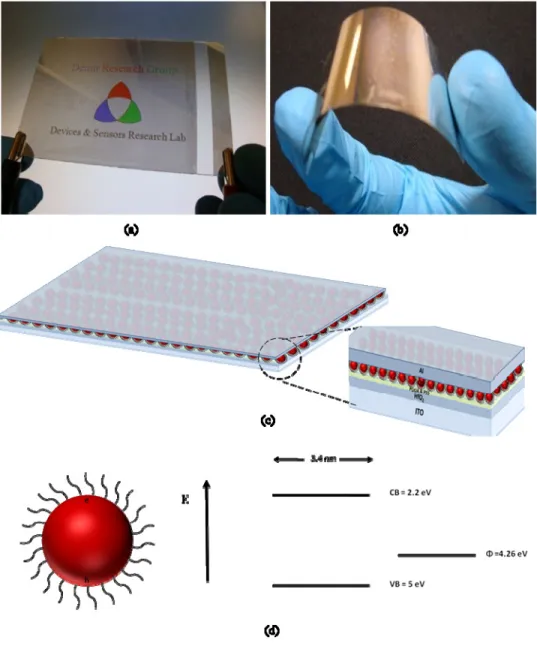
Fig. 1. (a) Large-area, semi-transparent, solution processed, light-sensitive nanocrystal skin (LS-NS) devices. Here is shown an 8 cm × 6 cm LS-NS device. (b) Photograph of a flexible LS-NS. (c) Schematics of a LS-NS structure consisting of a monolayer of TGA-capped CdTe nanocrystals (NCs) (shown as a monolayer of red dots here), along with a zoom-in illustrating the device structure of ITO/HfO2/PDDA + PSS/CdTe NCs/Al. (d) Band alignment of CdTe
NCs and Al contact. CdTe NC conduction band (CB) and valence band (VB) and the work function (Φ) of Al are shown on the energy diagram.
As a proof-of-concept demonstration, we fabricated a semi-transparent LS-NS device of 8 cm × 6 cm (i.e., 48 cm2) in size (see Fig. 1(a)) in which the maximum voltage buildup reaches 300 mV (under excitation at 350 nm with an optical power level of 0.153 mW/cm2 without applying any external bias). To deposit a NC monolayer on the substrate, colloidal dots were painted onto the substrate using spray coating, followed by a washing step to guarantee the formation of a monolayer. During device operation, through the increased interaction with the top contact immediately above the NC monolayer, more charge accumulation took place, which expectedly led to the measured high photosensitivity. Thanks to the device architecture
and utilization of solution processable NCs as the active semiconductor layer, our device has the potential to be constructed over even larger areas than the actual demonstrations here. LS-NS devices can also be made on a flexible substrate (e.g., ITO coated PET) if desired, as shown in a fabricated exemplary device in Fig. 1(b). The device architecture of ITO/HfO2/PDDA + PSS/CdTe NCs/Al is also sketched in Fig. 1(c). Here the Al contact serves as the hole acceptor for the NCs given the workfunction of Al and the band alignment of the NCs shown in Fig. 1(d). The experimental procedure and characterization results will be further discussed in detail in the following sections.
2. Experimental procedure
2.1 Colloidal synthesis
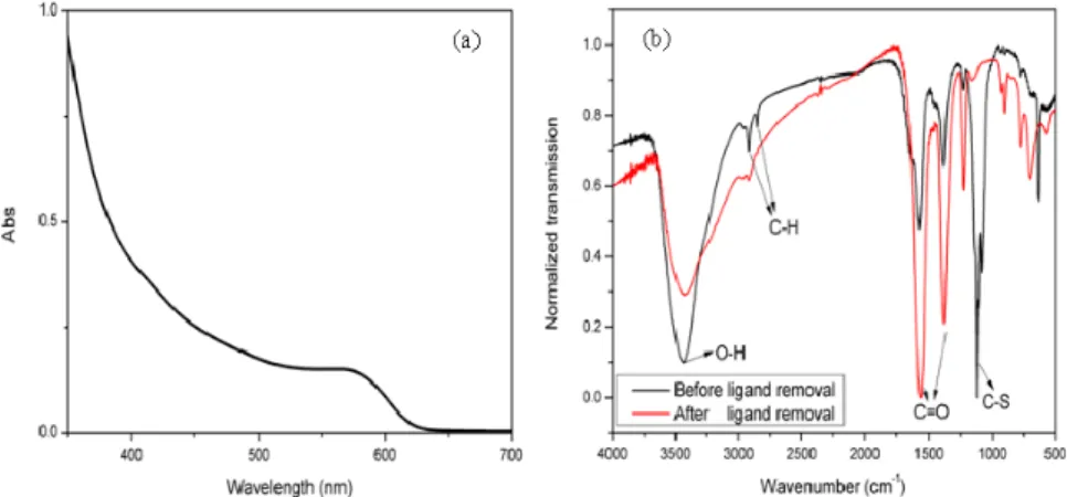
We synthesized water soluble (aqueous) CdTe NCs according to Ref [23]. In this method, 4.59 g of Cd(ClO4)2.6H2O was dissolved in 500 mL of Milli-Q water and 1.33 g TGA was added, followed by adjusting pH to 11.8-12.0. Then, H2Te gas obtained from the reaction of 0.8 g Al2Te3 with H2SO4 was passed through the solution with a slow Ar flow. Subsequently, the nucleation and growth of the NCs was initiated at 100 °C. Optical absorption spectrum of the resulting TGA-capped CdTe NCs is shown in Fig. 2(a). We observed the first exciton peak at around 560 nm (corresponding to a diameter of ~3.4 nm) with a photoluminescence decay lifetime of ~4 ns.
2.2 Ligand removal process
The control over the interface of NC surface is important because this helps to increase the device operation efficiency. Due to the ligands passivating the NC surface [24], charges see high potential barriers. To study the effect of ligands, we removed the TGA ligands from the NC surfaces by adding isopropanol into the CdTe NC solution and centrifuging the mixture. This process was carried out three times to remove sufficient ligands. During the layer-by-layer (LbL) film assembly, NC solution was then rigorously stirred in order to prevent the precipitation. The removal of the ligands from the NCs was confirmed by FT-IR spectroscopy. In the FT-IR spectrum, carbon-sulphur (C-S) bond is found to be present in the TGA-capped CdTe NCs, whereas it is practically absent (given the measurement sensitivity level) after the cleaning step (see Fig. 2(b)), indicating the successful substantial removal of the ligands.
Fig. 2. (a) UV-vis absorption spectrum of aqueous CdTe NCs at room temperature. (b) Normalized FT-IR spectra of TGA-capped CdTe NCs before and after the ligand removal.
2.3 Self-assembly (via dip-coating and spray-coating)
Layer-by-layer deposition technique can be used for fabricating multilayered thin films with a fine control over the film thickness. The LbL assembly relies on alternating adsorption of oppositely charged species, e.g., positively and negatively charged polyelectrolyte pairs [25]. For the purpose of controlled NC deposition, the NC monolayer of LS-NS devices was prepared using LbL deposition. To make film deposition via LbL assembly, a fully computerized dip-coater system was used. A monolayer of negatively charged CdTe NCs was deposited on top of alternating bilayers of strongly positive and negative polyelectrolyte polymers, deposited on HfO2 layer, and followed by a final positive polyelectrolyte layer. Poly(diallyldimethylammonium chloride) (PDDA) and poly(sodium 4-styrenesulfonate) (PSS) were used as the positively and negatively charged polyelectrolytes, respectively. The concentrations of these polyelectrolytes were 2 mg/mL in 0.1 M NaCl solution, since NaCl helps the polymer chain to relax on the surface. Water-soluble CdTe concentration was 4 μM. LbL films were prepared according to the standard cyclic procedure: (i) dipping of HfO2 -coated substrate into a PDDA solution for 5 min, (ii) rinsing it with water for 1 min, (iii) next dipping it into a solution of PSS for 5 min, and (iv) rinsing it with water for 1 min. This procedure was continued until four bilayers of PDDA and PSS composite were obtained. Finally, after deposition of one extra layer of PPDA and washing with water, the steps of dipping the sample into the dispersion of CdTe NCs for 20 min and rinsing with water again for 1 min were applied. Since the dip-coating technique has limitations for depositing CdTe NCs monolayer on a large-area substrate, we employed spray-coating technique to paint NCs over large areas, while keeping exactly the same sequence of monolayer depositions as described above.
2.4 Device fabrication and measurements
ITO film on a glass (or PET) substrate was washed using ultrasonication in a mixture of 2 mL Hellmanex in 100 mL water for 15 min, followed by ultrasonication in water (15 min), acetone (15 min) and isopropanol (15 min). Milli-Q water was used for all these steps and cleaning of the substrates. We then continued our fabrication by sputtering a 100 nm thick HfO2 dielectric film using atomic layer deposition (ALD). Subsequently, to deposit NCs, we used LbL self-assembly via dip coating to make a small device and spray coating to make a large device. At this step, we found that the formation of 4 bilayers of PDDA + PSS gives a uniform film with high surface coverage for the subsequent CdTe NC monolayer. Following each self-assembly step, the sample was washed to remove excess and unbound species of the substrate. Finally, a transparent, very thin, Al contact layer (of 15 nm in thickness) was laid down immediately on top of the CdTe NC monolayer via thermal evaporation (see Fig. 1(c)). In our measurements, we used Agilent Technologies B1500A semiconductor parameter analyzer and Xenon light source with an integrated monochromator. The illumination intensity was measured with an optical powermeter (Newport multi-function optical powermeter). In operation, the devices were connected to a shunt resistor (for example, 200 MΩ, or other values of choice), and no external bias was applied across the device.
3. Results and discussion
We performed electrical and optical characterizations of the LS-NS devices, including the measurements of photovoltage buildup, photodetection sensitivity, and photovoltage decay time. Because of the device architecture (sketched Fig. 1(c)), electrical charges cannot directly pass through the device due to the current blocking dielectric films (100 nm HfO2 film and 4 bilayers of PDDA + PSS with full surface coverage) so that the LS-NS device itself acts as a capacitor. With light illumination on the device, excitons are photogenerated in the NCs. Following the exciton formation, excitons are dissociated at the NC-Al interface and the holes are transferred and accumulated at the Al side due to Al workfunction and
HOMO/LUMO band alignment of the NC layer as shown in Fig. 1(d). As a result, Al layer favors hole accumulation given the interfacing NC monolayer [26]. Therefore, in the LS-NS device, Al acts as a hole acceptor, which leads to positive charge accumulation in the top Al contact, while electrons tend to stay in the NCs. Once separated, these charges are further capacitively held across the device; these are mainly the stored charges (but not the trapped charges). However, due to the photocharging effect, some of the electrons also get trapped inside the NC deep trap states; these are the long-lived trap states.
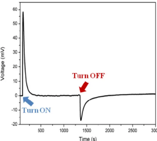
The operation of our device is experimentally shown in Fig. 3. With starting the light illumination, we first observe that there is a net potential buildup and, after reaching a peak point, this voltage buildup appears to diminish over time until it reaches a steady state in the presence of light illumination. At the steady state, when the light is switched off, a negative potential appears, which comes back to the initial point after some short time. The observed operational mechanism of the LS-NS device is based on the photovoltage buildup rather than the immediate charge collection. This operation does not require external biasing. To understand the operating principle of the device, it is worth pointing out that the non-trapped charges, which are stored capacitively across the LS-NS device, continuously decay because of the shunt resistor connected to the device with the instantaneous RC decay of the whole circuitry (the device + shunt resistor). The device capacitance also changes in time, which is further characterized and separately explained later in the paper. Also, there exist trapped charges, beside the exponentially decaying stored ones. Simultaneously, the external circuitry tends to neutralize the trapped charges in the NCs for eventually obtaining charge neutrality across the device. With light impinging on the device, the transient response reaches a peak, at which these opposing components become equal to each other and balance each other. The net photovoltage buildup appears to decay after this point. By switching off the light at the steady state level (see Fig. 3), the net potential goes negative. This is the potential of the trapped charges.
Fig. 3. Changes in the voltage buildup in time via switching the incident light on and off (with 0.153 mW/cm2 at 350 nm), marked with respective blue and red arrows.
While the light is on, some of the trapped charges draw holes from the Al contact to ensure the neutral state of the device. At the point when light is turned off, since there are no accumulated holes on the Al anymore, the net voltage reaches the lowest negative level and starts to recover and goes back to the zero level. This behavior shows the effect of trapped charges inside the NCs and the time taken to sweep out these charges. This indicates that the LS-NS device has a memory effect. As an interesting feature, LS-NS devices can therefore be also used to give information directly about the total amount of incident light power
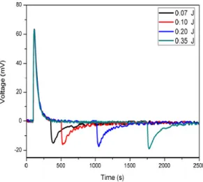
impinging on the device within a certain exposure period of time. This corresponds to the total incident optical energy to which LS-NS has been exposed. We found that the magnitude of the negative voltage appearing after switching the light off, which is directly proportional to the number of trapped electrons inside the NCs, change accordingly in response to changing light exposure time. This is due to proportional photocharging during the period of light exposure as seen in Fig. 4. However, this will work provided that the trap states in the NCs are not yet fully occupied and there are still more trap states available.
Fig. 4. Effect of photocharge trapping inside the NCs as the incident light shines continuously on the nanocrystals skin for different periods of time at 350 nm (0.175 mW/cm2). Here the
total of incident optical energy given in the legend is the amount of incident optical power multiplied by the exposure time and the exposure area.
For a detailed understanding of the device operating principle, we further studied the LS-NS operation by systematically varying the excitation wavelength and illumination intensity. The voltage buildup variation in response to excitation with different intensities at different wavelengths is shown in Fig. 5(a). We observed a higher voltage buildup at a shorter excitation wavelength, accompanied with a larger negative voltage after switching off the incident light. Due to the stronger optical absorption of CdTe NCs at shorter optical wavelengths, the voltage buildup is expected to increase with decreasing excitation wavelength. Essentially, this is because there are more electron and hole states available in a NC at a larger photon energy. This implies that a NC can absorb a larger number of photons at higher photon energies (i.e., at shorter wavelengths), photogenerating more electrons and holes under optical illumination at the same intensity level compared to longer wavelength excitation. This is in strong agreement with the profile of optical absorption spectrum of CdTe NCs (see Fig. 2(a)).
We also observed that the device exhibits a larger negative voltage at a shorter excitation wavelength due to the increased number of trapped charges, again owing to the increased optical absorption. It also takes more time to relax this increased number of charges in the absence of light as shown in Fig. 5(a). Similarly, Bulović et al. reported a decreasing external quantum efficiency of their cycled devices (NC-LEDs) as a result of charging of the NCs by trapped electrons over time [27]. We can measure the trap charge density in our devices, using the negative voltage value and the time required to recover after the light exposure is stopped.
Next, a meaningful figure-of-merit has been formulated to evaluate photodetection sensitivity of our device. Here we used the generic definition of the sensitivity as the ratio of electrical output signal to the optical input signal. Adapting this definition for the LS-NS
devices, the photodetection sensitivity (S) is given by the ratio of photovoltage buildup to the incident optical power (i.e., S = V/P, where V is the photogenerated voltage (in V) and P is the optical power (in W) impinging on the device). Figure 5(b) presents the sensitivity of the LS-NS device as a function of the excitation wavelength, with an increasing trend towards shorter wavelengths in agreement with the discussions above.
Fig. 5. (a) Variation of the voltage buildup at different excitation wavelengths and intensity levels. Light was turned off after reaching the peak point. (b) Corresponding sensitivity curve of the LS-NS device as a function of excitation wavelengths.
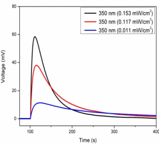
We also studied the effect of varying incident power on the voltage buildup at a fixed wavelength (in this case, 350 nm). We observed that, with increasing power, the photosensitivity decreases while the response time grows shorter. This is because of the decreased RC, which means faster response time and decreased sensitivity (Fig. 6).
Fig. 6. (a) Response time increases with the decreasing power since both deeper and shallower states saturate and (b) increasing illumination, resulting in decreased sensitivity because of filling the long-lived trap states. Arrows indicate the point in time when the light was turned off.
Furthermore, we observed that the RC decay kinetics changes over time in LS-NS devices (see Fig. 7). While the shunt resistance (R) is fixed at 200 MΩ, the RC decay time constant decreases with time because of the change in the capacitance of the device. This change in the capacitance is attributed to the variation in the effective dielectric constant of the NC layer and thus the overall capacitance of the LS-NS device. The decreasing device capacitance can explain the reduced charge accumulation in the presence of light over time, which then results
in a lower voltage buildup. Likewise, after reaching the peak point (as in Fig. 3), the decrease in the device capacitance speeds up the RC decay, which is in correlation with the data summarized in Table 1.
Fig. 7. RC decay rate changing in time by turning the incident light on and off at different intensity levels at 350 nm.
Table 1. Various device parameters including RC decay time constant (τ), effective device capacitance (C), and effective dielectric constant of CdTe NCs (εCdTe)) obtained from Fig.
7, when the shunt resistance is fixed at 200 MΩ. P represents the excitation power level
(of the Xenon lamp) incident on the device.
Positions in
Fig. 7 P = 0.175 mW P = 0.117 mW P = 0.011 mW
τ (s) C (nF) εCdTe τ (s) C (nF) εCdTe τ (s) C (nF) εCdTe
(1) 7.56 37.80 5.3 7.76 38.80 8.6 7.91 39.55 16
(2) 6.57 32.85 1.6 6.93 34.65 2.2 7.53 37.65 4.9
(3) 5.24 26.20 0.7 5.95 29.75 0.9 6.82 34.10 2.0
(4) 4.65 23.25 0.5 5.06 25.30 0.6 6.08 30.40 1.1
(5) 3.62 18.10 0.3 4.34 21.70 0.4 5.64 28.20 0.9
From Table 1, we observe that the illumination intensity also changes the RC decay time constant. We found that the slowest one belongs to the lowest intensity level. This is in agreement with the potential buildup changing with the illumination intensity when the light illuminates the device continuously (Fig. 8). The increased incident power results in a faster decrease, implying that the effective dielectric constant of NCs and thus the device capacitance are increasingly more decreased. Therefore, the voltage buildup under higher power excitation drops faster after reaching the peak point compared to those at the lower optical intensity levels.
Fig. 8. Variation of voltage buildup with time for different illumination intensity levels.
In the NCs, ligands act as the stabilizers by preventing them from agglomeration and precipitation. However, when we make devices of these NCs, ligands can suppress the charge transport. It therefore makes sense to consider that the substantial removal of ligands may increase charge transport and voltage buildup. This means that it is better to remove most of the ligands from NCs before making a device out of them. To demonstrate the effect of ligand removal, the LS-NS devices were fabricated using ligand-removed CdTe NCs. It is found that these devices with the substantial NC ligand removal show a higher voltage buildup (104 mV), which indicates higher photosensitivity compared to the case of NC devices with the ligands (60 mV) at the same intensity level. This leads to a large sensitivity enhancement factor of 73%, together with a 3-fold faster response with respect to the case of using ligands. Ligand-removed NC devices also exhibit more trapped charges. Figure 9(a) shows that when ligands are removed, trapped charges can also be released much faster than the case with the ligands. Also, it is expected the change in the device capacitance be faster than that in the case of ligands, which is also confirmed experimentally in Fig. 9(b).
Fig. 9. (a) Variation of voltage buildup with time for 0.175 mW/cm2 at 350 nm and (b) RC
decay change in time by turning the incident light on and off for 0.153 mW/cm2 at 350 nm
Sensitivity and fast response time are desirable parameters for different photosensing applications. However, there is a tradeoff between them, and thus improving one worsens the other. For instance, for a device to be compatible with video-frame-rate imaging, a temporal response in the order of 50 ms is necessary. In the case of LS-NS devices, by decreasing the shunt resistance (e.g., from 200 MΩ to 100 MΩ, 50 MΩ, 1000 KΩ, and 360 KΩ), it is possible to speed up the response time (from 8.0 s to 4.4 s, 2.4 s, 720 ms, and 300 ms, respectively, for an excitation intensity of 0.175 mW/cm2) as expected. For the same optical power, in the case of ligand-removed LS-NS devices, respectively faster RC decay time constants of 4.7 s, 2.4 s, 1.4 s, 220 ms, and 90 ms were observed. On the other hand, by increasing the shunt resistance (which was set ~200 MΩ in our previous characterizations) would in fact enhance the sensitivity, but this would come at the cost of slowing its temporal response time (due to the increased RC decay time constant). Therefore, the response time of LS-NS devices need to be adjusted in regards to the requirements of a specific application.
The LS-NS devices exhibit reasonably high photosensitivity in comparison to typical NC photodetectors. In the case of LS-NS devices, we calculate the minimum noise equivalent intensity to be 1.94 μW/cm2 for the devices with the ligands and 0.443 μW/cm2 when ligands are removed, which is comparable to the solution-cast NC photodetectors reported previously [28]. This, in addition to the adjustable response time, makes the LS-NS platform a promising one for photosensing applications.
4. Conclusion
In conclusion, we demonstrated highly efficient, semi-transparent, large-area, solution processable NC-based photosensors employing only single monolayers of NCs. These devices operate on the basis of photogenerated charge accumulation for which there is no need for external biasing (though an external bias can optionally be applied to quickly reset the system if desired). The monolayer of CdTe NCs, placed exactly underneath the metal contact without any transit intervening layer, results in close interaction enabling high photosensitivity and high stability under ambient conditions because of the device architecture sealing the NC monolayer. Furthermore, this device architecture is advantageous in terms of using a small amount of NC materials and making the device transparent with sufficient partial optical absorption. With the ligand removal, we observed a substantial enhancement of ~73% in the light sensitivity and a 3-fold faster response with respect to the case of using ligands. Also, we obtained a significant decrease in the minimum noise equivalent intensity by a factor of 4.4 in the case of ligand-removed NC devices (0.443
μW/cm2) compared to the devices without ligand removal (1.94 μW/cm2). High photosensitivity, adjustable response time, and memory effect make this LS-NS platform suitable for different optoelectronic applications including UV and visible sensing, e.g., in smart phones. Also, the ability to make large-area LS-NS devices via spray coating at low cost makes them potentially very interesting for smart windows and light-sensitive walls. Acknowledgment
We gratefully acknowledge the financial support in part by ESF EURYI, EU FP7 Nanophotonics4Energy NoE, and TUBITAK under the Project No. EEEAG 110E217, 111E186, and 112E183 and in part by NRF-CRP6-2010-02 and NRF RF 2009-09. HVD acknowledges additional support from TUBA-GEBIP.