NOVEL LIGHT-SENSITIVE
NANOCRYSTAL SKINS
A THESIS
SUBMITTED TO THE INSTITUTE OF MATERIALS SCIENCE AND NANOTECHNOLOGY
AND THE GRADUATE SCHOOL OF ENGINEERING AND SCIENCE OF BILKENT UNIVERSITY
IN PARTIAL FULLFILMENT OF THE REQUIREMENTS FOR THE DEGREE OF
MASTER OF SCIENCE
By
Shahab Akhavan
July, 2013
I certify that I have read this thesis and that in my opinion it is fully adequate, in scope and in quality, as a thesis for the degree of Master of Science.
Assoc. Prof. Dr. Hilmi Volkan Demir (Supervisor)
I certify that I have read this thesis and that in my opinion it is fully adequate, in scope and in quality, as a thesis for the degree of Master of Science.
Assoc. Prof. Dr. DönüĢ Tuncel
I certify that I have read this thesis and that in my opinion it is fully adequate, in scope and in quality, as a thesis for the degree of Master of Science.
Prof. Dr. Oğuz Gülseren
Approved for Graduate School of Engineering and Science
Prof. Dr. Levent Onural
ABSTRACT
NOVEL LIGHT-SENSITIVE NANOCRYSTAL SKINS
Shahab Akhavan
M.S. in Materials Science and Nanotechnology Supervisor: Assoc. Prof. Dr. Hilmi Volkan Demir
July, 2013
Light sensing devices traditionally made from crystalline or amorphous silicon, operating at the visible and near-infrared wavelengths, have led to a multibillion-dollar annual market. However, silicon faces various limitations including weak detection at long wavelengths (insufficient beyond 1.1 µm) with a cut-off at short wavelengths (in the ultraviolet) and small-area applications. On the other hand, solution-processed semiconductor nanocrystals (NCs), also known as colloidal quantum dots, offer large-area light sensing platforms with strong absorption cross-section. In this thesis we propose and demonstrate a new class of large-area, semi-transparent, light-sensitive nanocrystal skin (LS-NS) devices intended for large-surface applications including smart transparent windows and light-sensitive glass facades of smart buildings. These LS-NS platforms, which are fabricated over areas up to many tens of cm2 using spray-coating and several cm-squares using dip-spray-coating, are operated on the basis of photogenerated potential buildup, as opposed to conventional charge collection. The close interaction of the monolayer NCs of the LS-NS with the top interfacing metal contact results in highly sensitive photodetection in the absence of external bias, while the bottom side is isolated using a high dielectric spacing layer. In operation, electron-hole pairs created in the NCs of the LS-NS are disassociated and separated at the NC monolayer - metal interface due to the difference in the workfunctions. As a result, the proposed LS-NS platforms perform as highly sensitive photosensors, despite using a single NC monolayer, which makes the device semi-transparent and reduces the noise generation.
Furthermore, because of the band gap tunability, it is possible to construct cascaded NC layers with a designed band gap gradient where the NC diameters monotonically change. Here we present the first account of exciton funneling in an active device, which leads to significant performance improvement in the device. We show highly photosensitive NC skins employing the exciton funneling across the multiple layers of NC film. To further enhance the device photosensitivity performance, we demonstrate embedding plasmonic nanoparticles into the light-sensitive skins of the NCs. In addition, we exhibit the LS-NS device sensitivity enhancement utilizing the device architecture of semi-transparent tandem skins, the addition of TiO2 layer for increased charge
carrier dissociation, and the phenomenon of multiexciton generation in infrared NCs. With fully sealed NC monolayers, LS-NS is found to be highly stable under ambient conditions, promising for low-cost large-area UV/visible sensing in windows and facades of smart buildings. We believe the findings presented in this thesis have significant implications for the future design of photosensing platforms and for moving toward next generation large-surface light-sensing platforms.
Keywords: Quantum dots, nanocrystals, plasmonic nanostructures, TiO2,
multiexciton generation, light sensing, time resolved fluorescence, nanofabrication.
ÖZET
NANOKRĠSTAL TABANLI IġIĞA DUYARLI
YENĠLĠKÇĠ YÜZEYLER
ShahabAkhavan
Malzeme Bilimi ve Nanoteknoloji Yüksek Lisans Tez Yöneticisi: Doç. Dr. Hilmi Volkan Demir
Temmuz, 2013
Günümüzde kristal veya amorf tabanlı silikondan yapılan ıĢığa duyarlı aygıtlar en çok kullanılan ıĢık sensörleridir. Bu aygıtlar görünür ve kızılötesi bölgelerinde çalıĢırlar ve yıllık birkaç milyar dolarlık bir markete sahiptirler. Fakat silikonun sınırlı malzeme özellikleriden dolayı, ıĢığa duyarlı aygıtlarda zayıf hassasiyete (kızılötesinde ve morötesinde) sahip olmaktadır ve üretim teknikleri sebebiyle bu aygıtlar sadece ufak alanlarda üretilebilmektedirler. Alternatif olarak, yarı iletken nanokristaller, aynı zamanda kolloidal kuvantum noktacıkları olarak da bilinirler, farklı ve üstün özellikleri ile son yıllarda ıĢığa duyarlı aygıtlar için ön plana çıkmıĢ yenilikçi malzemelerdir. Bu tip nanokristaller solüsyon bazlı üretime ve iĢlemeye uygundurlar ve kuvvetli optik soğurmaya sahiptirler. Bu tezde yeni bir tip ıĢık sensörü olarak, büyük alanlı, yarı-geçirgen ve ıĢığa duyarlı nanokristal yüzeyleri tasarlıdık ve geliĢtirdik. Bu tip nanokristal yüzeyler (kısaltma olarak LS-NS‟i kullanıyoruz) akıllı camlar ve akıllı bina cepheleri gibi geniĢ alanlı uygulamalara uygundur. LS-NS‟ler onlarca cm2 büyüklüğündeki alanlara sprey kaplması yöntemi ile, birkaç cm2 büyüklüğündeki yüzeylere ise daldırmalı kaplama yöntemi ile kaplanabilir ve üretilebilir. LS-NS‟lerin çalıĢma prensibi ıĢık ile elektriksel gerilim yaratımına dayanmaktadır ve bu klasik fotosensörlerin fotoakım yaratımı prensibinden farklıdır. LS-NS genel olarak paralel tabakalı kondansatöre benzemektedir. Üst metal katmanın altında tek bir nanokristal katmanı içerir. Alt iletken kısım ise
ile ayrılmıĢtır. Nanokristal katmanının üst metal ile etkileĢimi sayesinde dıĢarıdan bir gerilimi uygulamaksızın yüksek ıĢık hassasiyeti elde edilir. IĢık ile nanokristallerin içinde oluĢturuluan elektron-deĢik çiftleri metal-nanokristal arayüzeyinde farklı metal ve nanokristalin farklı elektonegativiteleri sebebiyle bir birinden kopar ve ayrıĢır ve bu ayrıĢma potansiyel fark, olarak ölçülebilir. LS-NS platformu tek bir nanokristal katmanı içermesine rağmen yüksek hassasiyette ıĢık duyarlılığına sahiptir, ayrıca yarı-geçirgen yapılabilir ve gürültü seviyesi azaltılabilir. Nanokristallerin ıĢıma dalga boylarının kolayca ayarlanabilir olması ile basamaklı yapıda nanokristal içeren dizaynlar yapılmasına olanak sağlamıĢtır. Bu sayede ıĢık ile oluĢturulan elektron-deĢik çiftleri yüksek enerjili nanokristallerden düĢük enerjili nanokristallere doğru verimli Ģekilde aktarılabilmiĢtir. Bu tip eksiton taĢınımı ilk defa aktif bir aygıtta bu tezde kullanıldı. Bu sayede eksiton taĢınımını kullanan çok katmanlı nanokristal yapıları ile hassasiyeti artırılımıĢ LS-NS‟leri gösterdik. Aygıtların hassasiyetini daha da artırmak için plasmonik nanoparçacıkların katkılandırıldığı LS-NS‟ler tasarladık. Yanı sıra yarı-geçirgen LS-NS‟lerin ardarda dizilmesi ile birleĢik aygıt yapıları ürettik, bunlara titanyum oksit katmanı ekleyerek yük ayrıĢımını artırılması sağldık. Ayrıca çoklu eksiton yaratımı prensibi ile kızılötesire hassas nanokristaller kullanarak verimlilik artıĢı gösteridik. LS-NS‟ler tamamen izole edildiklerinden ortam koĢullarından etkilenmediklerini ve karalı oldukları gördük. Tüm bu özellikler, LS-NS‟leri ucuz, geniĢ alanlı ve ıĢık tayfına duyarlı (morötesi, görünür ve kızılötesi) ıĢık sensörleri yapmaktadır ve bu özellikleri onları akıllı camlarda ve akıllı bina cepheleri gibi alanlar için uygun yapmaktadır. Bu tezde gösterilen nanokristal tabanlı ıĢığa hassas yüzeyler gelecekteki ileri nesil ıĢık duyarlı platformlar için gelecek vaadetmektedir.
Anahtar kelimeler: Kuvantum noktacıkları, nanokristaller, plasmonik
nanoyapılar, TiO2, çoklu eksiton yaratımı, ıĢık hassasiyeti, zaman çözünürlü
Acknowledgements
I would like to thank my supervisor Assoc. Prof. Dr. Hilmi Volkan Demir for his endless support during my professional experience with him. Through these years, I have learned a lot from him both technically and personally. I would like to thank him for his great contributions and guidance.
Also my special thanks go to Assoc. Prof. Dr. DönüĢ Tuncel and Prof. Dr. Oğuz Gülseren for their kind support and also giving useful comments and suggestions as a member of my thesis committee.
This thesis would not be possible without our good friends and colleagues. First, I would like to thank all past and present Demir group members for being always helpful and friendly to me. Without your friendship and support, this thesis would not have been possible. I learned a lot from you and I am really proud to have such a selection of very nice people to be my best friends. Specially, I would like to thank Dr. Evren Mutlugün, Dr. Sedat Nizamoğlu, Dr. Emre Sarı, Burak Güzeltürk, and Talha Erdem from whom I have learned my basic lab skills and they always responded whenever I asked for help. I would like to acknowledge my friends Dr. Rohat Melik, Dr. Vijay Kumar Sharma, Dr. Dr. Ludwig P. Hernandez-Martinez and Dr. Urartu Ö. ġ. ġeker, Özgün Akyüz, Emre Ünal, and Dr. Nihan KoĢku Perkgöz. And now comes my officemates. I cannot forget the happy times we had there. I would also very much like to acknolwledge Can Uran, Yusuf KeleĢtemur, Ahmet Fatih Cihan, Kıvanç Güngör, Aydan Yeltik, Ġbrahim Akcalı, Halil Akcalı, Mehmet Zafer Akgül, Sayım Gökyar, Akbar Alipour, Somayeh Fardindoost, Berkay Bozok, Ozan Yerli, Veli Tayfun Kılıç, Dr. Gökçe Küçükayan, Muammer Yasin Hacısalihoğlu, Erdal Gönendik, Mustafa Akın Sefünç, Yasemin CoĢkun, Cüneyt Eroğlu, Onur Akın, Onur Erdem, and Togay Amirahmadov for their wonderful friendship and collaboration.
I would like to thank engineers and laboratory staff at UNAM who made our lives easier all the time.
I would also like to thank my parents for their endless love and support which helped me a lot to achieve my goals since my childhood. I would also like to thank my sister for always being kind to me and always next to me whenever I need her along with her enormous patience and love.
Table of Contents
1. INTRODUCTION ... 1
2. SCIENTIFIC BACKGROUND ... 6
2.1NANOSTRUCTURED MATERIALS FOR PHOTON DETECTION ... 6
2.2FUNDAMENTALS OF SURFACE PLASMONS ... 11
2.3FÖRSTER RESONANCE ENERGY TRANSFER ... 13
3. SEMICONDUCTOR NANOCRYSTALS ... 15
3.1CDTE NANOCRYSTAL SYNTHESIS ... 16
3.2ASSEMBLING OF SEMICONDUCTOR NANOCRYSTALS ... 18
4. LARGE-AREA SEMI-TRANSPARENT LIGHT-SENSITIVE NANOCRYSTAL SKINS ... 20
4.1INTRODUCTION ... 20
4.2EXPERIMENTS AND RESULTS ... 24
5. PLASMONIC LIGHT-SENSITIVE SKINS OF NANOCRYSTAL MONOLAYERS ... 36
5.1INTRODUCTION ... 36
5.2DEVICE PREPARATION AND CHARACTERIZATION ... 37
5.3RESULTS AND DISCUSSIONS ... 43
6. TANDEM PHOTOSENSITIVE NANOCRYSTAL SKINS ... 51
6.1INTRODUCTION ... 51
6.2RESULTS AND DISCUSSIONS ... 52
7. NANOCRYSTAL SKINS WITH EXCITON FUNNELING FOR PHOTOSENSING ... 58
7.1INTRODUCTION ... 58
7.2RESULTS AND DISCUSSIONS ... 61
8. PHOTOSENSITIVITY ENHANCEMENT IN SEMI-TRANSPARENT LIGHT-SENSITIVE SKINS OF NANOCRYSTAL MONOLAYERS WITH ELECTRON TRANSFER TO TIO2 ... 69
8.1INTRODUCTION ... 69
8.2EXPERIMENTS: ... 70
8.3RESULTS AND DISCUSSIONS: ... 73
9. MULTIPLE EXCITON GENERATION AND CHARGE ACCUMULATION FROM PHOTOSENSORS OF CDHGTE MONOLAYER NANOCRYSTALS ... 79
9.1INTRODUCTION ... 79
9.2EXPERIMENTS ... 80
9.3RESULTS AND DISCUSSIONS ... 81
List of Figures
Figure 2.1.1 Energy levels of bulk materials which are mostly used in NCs synthesis [28]. ... 7 Figure 2.1.2 Energy-level alignment in three different core/shell cases [32]. ... 8 Figure 2.1.3 Device structure of ultrasensitive solution-cast quantum dot
photodetector [19]. ... 9 Figure 2.1.4 A schematic representation of the photodiode device architecture
[21]. ... 10 Figure 2.2.1 Schematic representation of electric field due to an incident wave
and creation of oscillation as the electrons move back and forth. ... 12 Figure 2.3.1 Dependence of the FRET efficiency on r/R0. ... 14
Figure 3.1.1 CdTe nanocrystal synthesis setup. ... 16 Figure 3.1.2 Photoluminescence and UV-vis absorption spectra of as-synthesized aqueous CdTe NC solutions at room temperature. ... 17 Figure 3.1.3 Normalized FT-IR spectra of TGA-capped CdTe NCs before and
after the ligand removal. ... 18 Figure 3.2.1 Picture of our computerized dip-coater system. ... 19
Figure 4.1.1 (a) Large-area, semi-transparent, solution processed, light-sensitive nanocrystal skin (LS-NS) devices. Here is shown a 8 cm 6 cm LS-NS device. (b) Photograph of a flexible LS-NS. (c) Schematics of a LS-NS structure consisting of a monolayer of TGA-capped CdTe nanocrystals (NCs) (shown as a monolayer of red dots here), along with a zoom-in illustrating the device structure of ITO/HfO2/PDDA+PSS/CdTe NCs/Al.
(d) Band alignment of CdTe NCs and Al contact. CdTe NC conduction band (CB) and valence band (VB) and the work function (Φ) of Al are shown on the energy diagram. ... 23 Figure 4.2.1 Changes in the voltage buildup in time via switching the incident
light on and off (with 0.153 mW/cm2 at 350 nm), marked with respective blue and red arrows. ... 27 Figure 4.2.2 Effect of photocharge trapping inside the NCs as the incident light
shines continuously on the nanocrystals skin for different periods of time at 350 nm (0.175 mW/cm2). Here the total of incident optical energy given in the legend is the amount of incident optical power multiplied by the exposure time and the exposure area. ... 28 Figure 4.2.3 (a) Variation of the voltage buildup at different excitation
wavelengths and intensity levels. Light was turned off after reaching the peak point. (b) Corresponding sensitivity curve of the LS-NS device as a function of excitation wavelengths. ... 30 Figure 4.2.4 (a) Response time increases with the decreasing power since both
deeper and shallower states saturate and (b) increasing illumination, resulting in decreased sensitivity because of filling the long-lived trap states. Arrows indicate the point in time when the light was turned off. ... 31
Figure 4.2.5 RC decay rate changing in time by turning the incident light on and off at different intensity levels at 350 nm. ... 32 Figure 4.2.6 Variation of voltage buildup with time for different illumination
intensity levels. ... 33 Figure 4.2.7 (a) Variation of voltage buildup with time for 0.175 mW/cm2 at 350
nm and (b) RC decay change in time by turning the incident light on and off for 0.153 mW/cm2 at 350 nm wavelength in the case of ligand-removed LS-NS devices. ... 34 Figure 5.2.1 SEM images of four silver nanoparticle films with 10 nm mass
thickness on 50 nm HfO2, film annealed at different temperatures and
durations. (a) Not annealed, (b) annealed at 150 °C for 2 min, (c) annealed at 300 °C for 2 min, and (d) annealed at 300 °C for 20 min. ... 38 Figure 5.2.2 (a) Optical excitation spectra of silver nanoparticle films with a
mass thickness of 10 nm deposited at 0.3 Å/s evaporated rate annealed at different temperatures for different durations. (b) Optical extinction spectra of 10 nm thick silver nanoparticle film annealed at 300 °C for 20 min covered with 1 nm Al2O3, different number of PDDA and PSS bilayers, and
single monolayer of NC. ... 39 Figure 5.2.3 (a) Schematic illustration of a plasmonic light-sensitive nanocrystal
skin (LS-NS). (b) Surface plasmon resonance sensitization of Ag nanoparticle and band alignment of CdTe NC (3.7 nm in size) conduction band (CB), valence band (VB), and the workfunction (Φ) of Al and ITO. Hence, Ef demonstrates the Fermi level of CdTe NCs at equilibrium
condition. After the excitons are photogenerated (1), electrons are remained in the NCs while holes migrate to the Al side (2). ... 41
Figure 5.2.4 UV-vis absorption spectrum of aqueous CdTe NCs at room temperature. ... 42 Figure 5.3.1 Voltage buildup variations of LS-NS based on (a) four bilayers of
PDDA and PSS and (b) seven bilayers of PDDA and PSS for different excitation wavelengths. Solid line represents the plasmonic sample (PS) and dashed line represents the control sample (CS). ... 46 Figure 5.3.2 Comparison of the sensitivity of LS-NS device structure in the
absence and presence of plasmonic nanostructures based on (a) four bilayers, (b) seven bilayers, and (c) ten bilayers of PDDA and PSS separating bilayers. Insets figure presents the sensitivity enhancement factor vs. wavelength. ... 47 Figure 5.3.3 (a) Normalized extinction of simulated silver nanoparticles with
and without presence of spacing layer. (b) Electric field intensity distribution at the interface of HfO2 film and the silver nanoparticles. (c)
Electric field distribution along the interface of the spacing layer and air interface. (d) Cross-sectional 2D electric field intensity distribution along y-z plane. White dashed line coincides with the vertical line of figure 7(c) indicated with red dots. (e) Cross-sectional 2D electric field intensity distribution along x-z plane. White dashed line coincides with the horizontal line of figure 7(c) indicated with blue dots. All the color bars and scale bars are identical for the cross-sectional electric field maps. Scale bars correspond to 200 nm and color bar represents relative values of electric field intensity ranging from 0 to 2 in logarithmic scale. ... 49 Figure 6.2.1 (a) Schematic of the device architecture for solution processed
semi-transparent tandem photosensitive nanocrystal skins. (b) Absorption spectra of single colloidal CdTe and CdHgTe NCs monolayers………….53
Figure 6.2.2 (a) and (b) Variation of photovoltage buildup at different excitation wavelength and optical intensity for devices based on CdTe and CdHgTe, respectively. (c) Corresponding photovoltage buildup of tandem photosensitive nanocrystal skin………... 56 Figure 7.1.1 (a) Schematic of the photosensitive NC skins, consisting of closely
packed layers of ligand-free CdTe NCs. (b) Alignment of the conduction and valence bands of the CdTe NC layers and the workfunction of the Al contact. Each exciton tunnels through the layers because of a band gap gradient. ... 60 Figure 7.1.2 Photoluminescence and UV-vis absorption spectra of as-synthesized aqueous CdTe NC solutions at room temperature. ... 61 Figure 7.2.1 Experimental photovoltage buildup results of photosensitive NC
skins at different excitation wavelengths and intensity levels based on (a) a single layer of NCs, (b) five layers of NCs of identical sizes, (c) five layers of NCs ranging from large to small, and (d) five layers of NCs ranging from small to large. ... 63 Figure 7.2.2 A comparison of the devices‟ corresponding sensitivities as a
function of excitation wavelength based on (a) a single layer of NCs, (b) five layers of NCs of identical sizes, (c) five layers of NCs ranging from large to small, and (d) five layers of NCs ranging from small to large. Inset figures present the devices‟ schematics and the direction of incident light. ... 65 Figure 7.2.3 Time-resolved PL decays of the five donor NC layer samples, the
five acceptor NC layer samples, and the five hybrid-layer samples. Insets show the first 20 ns parts of the decays. ... 66
Figure 7.2.4 Normalized photoluminescence spectra of five NC monolayers of different sizes on the glass. ... 67 Figure 8.1.1 (a) Energy band diagram and (b) schematic of the LS-NS device by
incorporating TiO2 layer. ... 70
Figure 8.2.1 Absorption spectra of 10 nm TiO2 on HfO2 coated glass. ... 71
Figure 8.2.2 Photoluminescence and UV-vis absorption spectra of as-synthesized aqueous CdTe NC solutions at room temperature. ... 72 Figure 8.3.1 Variations of the photovoltage buildup based on four bilayers
PDDA-PSS at different excitation wavelength (a) without TiO2 and (b)
with TiO2. Photovoltage buildup variation based on one bilayer PDDA-PSS
(c) without TiO2 and (d) with TiO2. ... 74
Figure 8.3.2 Sensitivity comparison of the LS-NS devices in the absence and presence of TiO2 layer for the structures based on (a) four bilayers
PDDA-PSS, and (b) one bilayer PDDA-PSS. ... 76 Figure 8.3.3 Time-resolved PL decays of the NCs in the absence and presence of
TiO2 layer based on different bilayers of polyelectrolyte polymers. The
arrow indicates the reduction in the lifetime of the NCs based on one bilayer of polyelectrolyte polymers from the structure without TiO2 to the
one with the TiO2 layer. ... 77
Figure 9.2.1 Absorption spectrum of NCs and device structure. (a) UV-vis absorption spectrum of aqueous TGA and MPA ligand CdHgTe and CdTe NCs at room temperature. (b) Schematic drawing of the light-sensitive nanocrystal skin structure. Monolayer CdHgTe NCs were formed through
Figure 9.3.1 (a) Voltage buildup behavior of LS-NS devices based on monolayer of TGA (solid line) and MPA (dashed line) ligand CdHgTe NCs at different wavelength. (b) Spectral sensitivity of two LS-NS devices corresponding to their voltage buildup and identical number of photons impinge on them. ... 83 Figure 9.3.2 Sensitivity of the LS-NS based on monolayer of CdTe NCs at
List of Tables
Table 4.2.1. Various device parameters including RC decay time constant (τ), effective device capacitance (C), and effective dielectric constant of CdTe NCs (εCdTe)) obtained from Figure 4.2.5, when the shunt resistance is fixed at 200
MΩ. P represents the excitation power level (of the Xenon lamp) incident on the device...32
To my parents who provided the
opportunities and for their love,
patience and understanding…
Chapter 1
Introduction
Imaging, remote sensing, optical communications, and spectroscopy are some of the important applications enabled by the detection of optical signals. A photosensitive material needs to absorb incident optical signals and convert them into electrical signals. Detection in the visible region is suitable for applications including spectroscopy and fluorescent biomedical imaging. In favor of the passive night vision [1, 2] and biomedical imaging for tumor detection [3, 4, 5] sensitive photodetection in the infrared region is required. Subsequently, multispectral imaging, which provides independent piece of information, is possible by combining visible and infrared wavelengths. However, due to the high fabrication cost and modest performance, their functionality is limited [6].
Light detection has traditionally been enabled by crystalline semiconductor photodetectors. In the last few decades, detectors made from silicon as photon-to-electron converter dominate the multibillion-dollar annual market [7]. The compatibility of the silicon electronics with silicon photodiodes enables low noise signal and multiplexing [8]. However, this technology faces some limitations. Silicon can absorb light relatively strongly only below 1.1 m in addition to the weak absorption over the entire spectrum at 500 nm the absorption of silicon can only exceed 104 cm-1 [9]. Furthermore, silicon may also
suffer the cross talk and blurring of optical signal problems due to the long lifetime and high mobility of the electron-hole pairs [10]. Consequently, materials that expand the absorption spectrum with a high absorption coefficient to decrease the semiconductor thickness to at least less than 100 nm are significantly required.
Solution-processed semiconductor nanocrystals (NCs) are of increasing interest for use in optoelectronic devices and offer advantages including low cost, flexibility, large device area, and spectral tunability based on the quantum size effect [11, 12]. In contrast to conventional epitaxial growth of lattice-matched semiconductors, such solution-processed optoelectronic materials provide promising convenient integration atop electronic substrates (e.g., using dip coating, spin coating and drop casting), where lattice mismatch problems do not arise. Therefore, these NCs are promising candidates for applications in diverse areas, such as in light-emitting diodes [13], solar cells [14], and photodetectors [15, 16] as well as for biolabeling [17] and biosensing [18].
Conventional photodetectors using NCs typically operate on the principle of collecting photogenerated charges, where an external bias must be applied for the charge collection. Recent research efforts increasingly focus on NC photodetectors that show a remarkable level of sensitivity [19] and short response times [20]. These photodetectors do, however, commonly exhibit high dark current, which results in high noise levels and limits the device‟s detection capabilities [21].
Our research interest mainly focuses on fabricating and developing novel highly sensitive photosensor structure. As an alternative architecture, NC skins offer the potential of high sensitivity for large-area applications because they operate on the principle of photogenerated voltage buildup in the absence of an external bias. With a single NC layer in the device structure, noise generation is significantly reduced, which enhances the device sensitivity [22].
In Chapter 1, we present a brief introduction to materials and NCs for optical detection. The importance and the use of NCs in optoelectronic applications are discussed here.
In Chapter 2, we provide a background on the nanostructured materials for photon detection. Furthermore, we introduce surface plasmon resonance of metal nanoparticles and the influence of size, shape and environmental medium on the plasmonic behavior. Hence, we present a brief background on the Förster resonance energy transfer and its mechanism.
In Chapter 3, we discuss the fundamental properties of NCs as promising materials for optoelectronic devices. Also, we explain the synthesis methods of CdTe NCs, along with their optical characterization.
In Chapter 4, we present and demonstrate a large-area, semi-transparent, light-sensitive nanocrystal skin (LS-NS) devices. These LS-NS platforms, which were fabricated over areas up to 48 cm2 using spray-coating and several cm-squares using dip-coating, are operated on the basis of photogenerated potential buildup, as opposed to conventional charge collection. In operation, close interaction of the monolayer NCs of the LS-NS with the top interfacing contact, while the bottom one is isolated using a high dielectric spacing layer, results in highly sensitive photosensing in the absence of external bias application.
In Chapter 5, we show that plasmonic nanoparticles are strong candidates to improve the electron-hole pair generation in NC-based devices. In particular, NC photosensors exhibit low performance toward long wavelengths, due to low optical absorption of NCs. Here, to enhance the device photosensitivity performance, embedding silver nanoparticles into the light-sensitive skins composed of the monolayer CdTe NCs was demonstrated. The deposited plasmonic silver nanoparticles increased optical absorption of the NC monolayer
over broadband (400-650 nm) spectral range were observed with a 2.6-fold enhancement factor around the localized surface plasmon resonance peak. To further predict the enhancement in sensitivity of the devices, we performed simulations using FDTD method. Our experimental results agree well with the theoretical calculations considering the near-field electric field enhancement in the vicinity of silver nanoparticles. Furthermore, we studied the distance dependent sensitivity of the resulting devices with silver nanoparticles incorporated into NC skins to reveal the effect of localized surface plasmons. In Chapter 6, we report the first colloidal NC-based tandem photosensitive skins. We fabricated the tandem photosensors which is composed of spray-coated monolayers of colloidal water soluble CdTe NCs and design the device to operate without applying any external bias. The top semi-transparent electrodes on each constituent junction accumulate holes while electrons are trapped inside the NCs. Subsequently, we have demonstrated that it is possible to enhance the device sensitivity for more that 100% and at the same time accelerate the response time compared to the single junction photosensitive devices.
In Chapter 7, we present the first account of exciton funneling in an active device, which leads to significant performance improvement in the device. Here we show highly photosensitive gradient NC skins based on the exciton funneling across the layers of NC film. Previously, this concept was demonstrated using layered NC films in the pioneering work of Franzl et al. [23]. To explore this proposition, we fabricated devices that rely on accumulating dissociated charges after photogenerating and funneling excitons. We demonstrate how funneling excitons along a gradually decreasing band gap gradient of the cascaded NC monolayers enhances photosensitivity of the device platform. We observed substantial improvements in the photosensitivity over a broadband spectral range (350-600 nm), with an approximately twofold enhancement factor along the entire operating wavelength range. To better understand and prove the presence of the exciton transfer process in the cascaded NC skins, we also
conducted time-resolved fluorescence measurements at the donor and acceptor wavelengths; the results confirmed the exciton transfer process in the NC gradient structure.
In Chapter 8, we show highly photosensitive NC skins based on the use of TiO2
as electron accepting material. In the absence of any external bias, some excitons may remain in the NCs layer where it was created and then tend to recombine leading lower voltage buildup. To explore this proposition, we fabricated devices that rely on accumulating dissociated excitons after photogenerating and transferring electrons to TiO2 while holes migrating to Al
contact. As a result, we demonstrate how the electron transfer to TiO2 thin film
in LS-NS enhances photosensitivity of the device platform. We observed substantial improvements in the photosensitivity over a broadband spectral range (350-475 nm), with an approximately 22% enhancement. To better understand and prove the presence of the electron transfer process from the CdTe NCs to the TiO2 layer, we also conducted time-resolved fluorescence
measurements; the results supported the existence of electron transfer from the NCs to TiO2 layer in light-sensitive skins.
In Chapter 9, we report a significant sensitivity enhancement making use of multiple exciton generation and subsequent charge accumulation per incident photon in photosensitive NC skins composed of a monolayer of near-infrared absorbing CdHgTe NCs. The 3.3-fold enhancement in sensitivity was observed at photon energies greater than 2.4 times of the CdHgTe NCs band gap. Implementing a control experiment, excitation of CdTe NC-based device did not show any enhancement through MEG due to the improper band gap of these NCs given the excitation wavelength.
Chapter 2
Scientific Background
2.1 Nanostructured Materials for Photon Detection
Colloidal semiconductor NCs, also known as colloidal quantum dots are made up of a few hundred to a few thousand atoms. Usually these materials are surrounded by an organic layer of surfactant molecules called as ligands [24, 25]. Their small size to a few nanometers (less than the Bohr radius) results in strong quantum confinement effect. This also increases the effective band gap due to the quantization of energy levels to discrete values. Subsequently, the sizes of the NCs influence their optical properties [26]. Optical properties of NCs also depend on their surface passivation. These surface passivated core NCs may result in surface trapped states acting as nonradiative channels reducing the fluorescence quantum yield. In order to improve the NCs‟ surface passivation, overgrowth with a shell of second semiconductor material has been the focus of significant research over the past two decades. It has been demonstrated that with coating the shell material it is possible to tune the emission and absorption spectra [27].
Regarding the band gap and relative position of electronic energy levels of the semiconductor, shell can have different functions. Electronic energy levels of bulk materials which are mostly used in NCs synthesis is given in Figure 2.1.1.
Figure 2.1.1 Energy levels of bulk materials which are mostly used in NCs synthesis [28].
Band alignment configurations can be distinguished in three cases known as type-I, reverse type-I, and type-II (see Figure 2.1.2). In the type-I case, when the band gap of the shell material is larger than the core, the electrons and holes are confined in the core. Usually, in order to passivate the surface of the core NCs which leads to improved emission, type-I is used. In this case, the shell passivates the core and reduces its dependency on the environmental changes such as oxygen or water molecules. Subsequently, stability of the NCs against photodegradation is enhanced. Moreover, the shell reduces the number of surface dangling bonds, which can act as trap states. In the reverse case, the band gap of the core material is larger than the shell one. Subsequently, depending on the shell thickness, electrons and holes are partially or completely confined in the shell. Subsequently, by changing the shell‟s thickness, the emission wavelength can be tuned [29, 30]. In these systems photostability can be enhanced by the growth of a second shell with a larger band gap [31]. In the last case, either the conduction-band edge or valence-band edge band gap of the shell is located in the band gap of the core. Because of the lower overlap of the
electron and hole wavefunctions, the photoluminescence (PL) decay of type-II is longer than type-I.
Figure 2.1.2 Energy-level alignment in three different core/shell cases [32].
For detection applications, NCs are attractive materials since they can easily be deposited with a variety of substrates. Although detectors made from silicon dominate the multibillion-dollar market for digital cameras and image sensors, they have some limitations. Silicon cannot absorb most of the infrared spectrum, since it absorbs wavelengths only below 1.1 m. Moreover, it has a small absorption coefficient over the entire spectrum. Subsequently, materials that can absorb light where silicon cannot are of intense interest. However, these materials preferably need to be compatible for integration with silicon, flexible, and large-area substrates.
NCs offer great potential with their superior properties. They are very promising for optoelectronic devices including light emitting diodes [33], solar cells [34], single photon detectors and emitters [35], infrared sensors [36], light convertors [37, 38, 39], and scintillators [40]. NCs can be synthesized using wet chemistry and processed from the solution phase [41], which enables solution processable optoelectronic devices at reduced costs, with the additional advantages of making flexible structures, if desired, and in large-area production in principle. NCs are very versatile and can be deposited essentially almost on any substrate using dip coating [42], spin coating [43], spray coating [44], and inject printing [45]. Additionally, NCs possess widely tunable optical absorption and emission
properties using the quantum size effect. Moreover, the strong confinement leads to various mechanisms in NC solids including variable-range hopping [46], slow carrier relaxation [47], and electron and hole interaction [48] and delocalization [49].
Solution-processed photodetectors are classified into two classes, photoconductors and photodiodes. In the photodetectors, one type of the carrier circulates through the external circuit for several times until it recombines with the opposite trapped carrier, which leads to high gain. If the transit time is longer than the recombination duration of photogenerated excitons, many of charges can pass through the circuit. In order to prolong the electron-hole pair recombination time, introducing traps in the colloidal NCs film can be used [50, 51, 52]. The physical mechanisms behind solution-cast photoconductive photodetector have attracted great interest since 2006 [19]. In this previous study, PbS colloidal NCs were coated over prefabricated planar electrode array. The device showed a large photoconductive gain, especially after removing the ligands (see Figure 2.1.3).
Figure 2.1.3 Device structure of ultrasensitive solution-cast quantum dot photodetector [19].
On the other hand, in the photodiodes, the photogenerated electrons and holes move to opposite electrical contacts (see Figure 2.1.4). These types of photodetectors can have fast response times. In photodiodes, difference in the material‟s Fermi levels leads to built-in potential. The internal field in the semiconductor depletion region separates the electrons and holes in opposite directions. To obtain high internal quantum efficiency, tlife should be larger than
textract, where tlife is the lifetime of excess charge carriers and textract is the time
taken to transport carriers to the contacts given by textract =L2/Vbi where L is the
contact separation, mobility of slower carrier and Vbi is the built-in potential
[53]. In conventional crystalline semiconductors, charges sweep a distance of 1m much faster than nanoseconds through a built-in potential of 1 V, due to their high mobility, which is in the range of 102 cm2Vs-1 and above. On the other hand, in solution-processed NCs charges sweep a distance of 100 nm with a built-in voltage of 1 V in the range of 100 ns-10 s, since they have much lower motilities in the range of 10-5-10-3 cm2Vs-1. However, thanks to the unusual long exciton lifetimes of some colloidal NCs (> 1s), excellent photodiode quantum efficiency can be obtained [54].
2.2 Fundamentals of Surface Plasmons
Localized surface plasmons (LSP) consist of the collective oscillations of free electrons spatially confined in metal nanoparticles under impinging electromagnetic radiation on resonance condition [55]. SP may appear in different forms such as freely propagating electromagnetic surface waves along metal surfaces and localized electron oscillations confined in metal nanoparticles. In this thesis, we will study the LSP generated in metal nanoparticles and used to enhance the device sensitivity in the spectral range especially where the photosensitivity is low.
The optical response of metal nanoparticles is due to the LSP resonance wavelength. As a result of SP, a strong electric field around the nanoparticle takes place, which vanishes exponentially by distance away from the nanoparticle [56]. LSP is strongly observed when the nanoparticle size decreases considerably, since electromagnetic field can penetrate into the particle. For Ag and Au metals, the penetration depth is around tens of nanometers. Subsequently, metal nanoparticles at this range should be obtained [57]. LSP generates polarization on the particle (sinusoidal varying electric field) and because of the Coulomb attraction force between the conduction electrons and fixed positive ions at the nucleus, a restoring force is generated [58]. As the electrons move back and forth, the restoring force gives rise to the oscillation (see Figure 2.2.1).
Figure 2.2.1 Schematic representation of the electric field due to an incident wave and creation of oscillation as the electrons move back and forth.
The frequency of this oscillation is called the SP resonance frequency. SP resonance is given as 2 3 0 e4 s e w m r (1)
where ɛ0 is the vacuum permittivity, me is the effective mass, rs radius of sphere.
As it is evident, resonance frequency is inversely proportional to the nanoparticle size [59].
LSP resonance frequency depends on the size, shape, and surrounding medium dielectric function. Ag and Au nanoparticles have frequencies corresponding to the visible region. On the other hand, Al and Hg have higher frequencies. The upper and lower size limits for Ag and Au to observe plasmonic effects is 100 and 5 nm, respectively. Ag and Au show strong SP resonance in the size range of 5-50 nm [60]. As the nanoparticle size increases, plasmon resonance makes red shift. Additionally, monodispersity of nanoparticle size distribution influences the plasmonic resonance peak. As the nanoparticles monodispersity increases, plasmon resonance peak become sharper. One of the other key factors effective on plasmon resonance is the shape of metal nanoparticles. They can be made in spherical, cubical and cylindrical. It has been reported that plasmon
resonance wavelength can be shifted from 400 to 670 nm as the spherical Ag nanoparticle changes to trigonal prism [61]. Moreover, different kinds of materials surrounding the nanoparticle can change the SP resonance spectrum. For example, the dielectric coating on film increase the refractive index of surrounding medium which cause a red shift in the plasmon resonance spectrum [62].
2.3 Förster Resonance Energy Transfer
Förster resonance energy transfer (FRET) is a nonradiative-type energy transfer that takes place between two resonance molecules in very close proximity. FRET has been especially used in biology to determine the distance between the molecules. In FRET, the donor molecule transfers its energy before being radiated as a photon emission. FRET occurs, when the donor emission spectrum overlap with the acceptor absorption spectrum. In this mechanism, the donor should have a high quantum yield, the acceptor should have a high extinction coefficient, and donor and acceptor should be in close proximity (less than 10 nm). In the case when the acceptor and donor molecules are less than 1 nm distance apart from each and, if their wavefunctions overlap, the exciton transfer occurs, which was first explained by the Förster theory.
To verify the Förster energy transfer, time resolved spectroscopy and steady state fluorescence measurement are used. In time resolved spectroscopy the mechanism is observed with the change in the donor lifetime. As the donor molecule feed the acceptor with its excitation energy, its lifetime decreases while the acceptor‟s increases. The rate of energy transfer has a r-6 dependency as given by Equation 2. 6 0 1 t D R k r (2)
where Kt is the rate of energy transfer, τD is the donor lifetime in the absence of
acceptor. R0 is the Förster radius at which the decay rate and transfer rate of the
molecule is equally probable and FRET efficiency is 50%. Förster radius can be found as follows:
1
2 4 6
0 0.211( Q J( ))D
R n (3)
Here κ2 is the orientation factor, n is the refractive index of the media, QD is the
quantum efficiency of the donor, and J (λ) is the overlap integral. As it can be seen from the Figure 2.3.1 FRET is effective when r is less than or equal to R0.
Chapter 3
Semiconductor Nanocrystals
Chemically synthesized NCs are considered as candidate materials promising for a wide range of optoelectronic applications because of their band gap tunability and solution processability, which facilitate integration with a variety of substrates at reduced costs over large-areas. As a result, light detection using these colloidal NCs has attracted significant attention in recent years. Our research group is also interested in colloidal NCs containing the elements cadmium, indium, and selenium, which may also be surrounded by a shell composed of sulphur or zinc.
Generally, synthesis of semiconductor NCs results in spherical-like crystalline structures with diameters ranging from one to ten nanometers. When the electrons and holes are trapped in the potential well of the NCs in three dimensions, quantum confinement effect takes place. Moreover, on the contrary to the bulk crystalline semiconductor in which the energy level is continuous, the energy levels in NCs become discrete via the reduction of crystal size to nanoscale. Moreover, the exciton binding energy is given as follows:
2 2 2 8 n n E mr (4)
where ħ is the reduced plank‟s constant, n is the quantum number, m is the effective mass and r is the radius of NC.
Subsequently, the quantum size effect is the main reason for shifting the NCs emission as their size changes. For instance, we obtain red emission for the larger NCs, while the emission is blue for the smaller NCs.
3.1 CdTe Nanocrystal Synthesis
We synthesized water soluble (aqueous) CdTe NCs according to Ref [63]. In this method, 4.59 g of Cd(ClO4)2.6H2O was dissolved in 500 mL of Milli-Q
water and 1.33 g TGA was added, followed by adjusting pH to 11.8-12.0. Then, H2Te gas obtained from the reaction of 0.8 g Al2Te3 with H2SO4 was passed
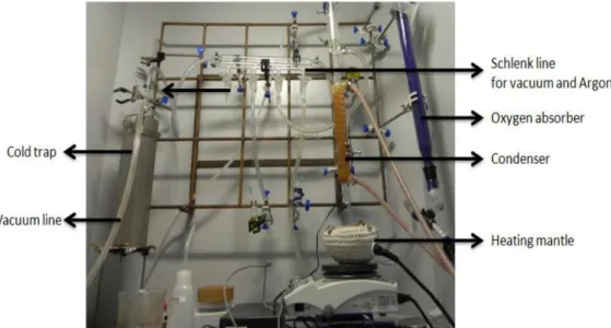
through the solution with a slow Ar flow. Subsequently, the nucleation and growth of the NCs was initiated at 100 0C. NCs start to grow as the solution starts boiling and gets bigger in size during this period. Synthesis setup used to synthesize CdTe NCs can be seen in Figure 3.1.1.
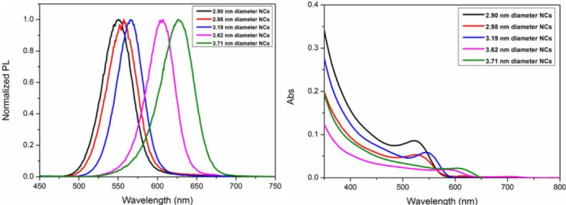
Fluorescence and optical absorption spectra of the resulting TGA-capped CdTe NCs are shown in Figure 3.1.2 and the NC diameters were calculated from their extinction spectra [32]. These diameters were 2.90, 2.98, 3.19, 3.62, and 3.71 nm, increasing the first excitonic peak wavelength as 525, 532, 545, 595, and 605 nm, respectively.
Figure 3.1.2 Photoluminescence and UV-vis absorption spectra of as-synthesized aqueous CdTe NC solutions at room temperature.
Furthermore, we found their photoluminescence decay lifetimes to be ~4 ns. After all, we use a rotary evaporator to increase the concentration and remove the extra amount of solvent. Hence, to further clean the solution from impurities, paper filters and size-selectively precipitation after several centrifuging steps are applied.
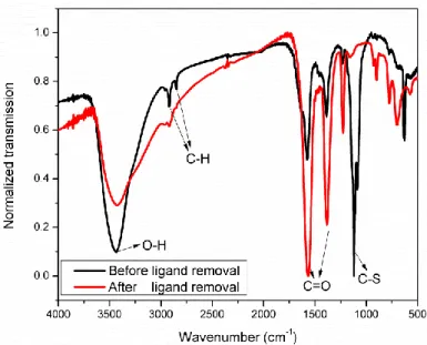
The control over the interface of NC surface is important because this helps to increase the device operation efficiency. Due to the ligands passivating the NC surface, charges see high potential barriers. To study the effect of ligands, we removed the TGA ligands from the NC surfaces by adding isopropanol into the CdTe NC solution and centrifuging the mixture. This process was carried out three times to remove sufficient ligands. During the layer-by-layer (LBL) film assembly, NC solution was then rigorously stirred in order to prevent the precipitation. The removal of the ligands from the NCs was confirmed by FT-IR
present in the TGA-capped CdTe NCs, whereas it is mostly absent after the cleaning step (see Figure 3.1.2), indicating the successful removal of the ligands.
Figure 3.1.3 Normalized FT-IR spectra of TGA-capped CdTe NCs before and after the ligand removal.
3.2 Assembling of Semiconductor Nanocrystals
LBL deposition technique can be used for fabricating multilayered thin films with a fine control over the film thickness. The LbL assembly relies on alternating adsorption of oppositely charged species, e.g., positively and negatively charged polyelectrolyte pairs [64]. For the purpose of controlled NC deposition, the NC monolayer of LS-NS devices was prepared using LBL deposition. To make film deposition via LBL assembly, a fully computerized dip-coater system was used (see Figure 3.2.1). A monolayer of negatively charged CdTe NCs was deposited on top of alternating bilayers of strongly positive and negative polyelectrolyte polymers, deposited on HfO2 layer, and
followed by a final positive polyelectrolyte layer. Poly(diallyldimethylammonium chloride) (PDDA) and poly(sodium 4-styrenesulfonate) (PSS) were used as the positively and negatively charged
polyelectrolytes, respectively. The concentrations of these polyelectrolytes were 2 mg/mL in 0.1 M NaCl solution, since NaCl helps the polymer chain to relax on the surface. Water-soluble CdTe concentration was 4 M. LBL films were prepared according to the standard cyclic procedure: (i) dipping of HfO2-coated
substrate into a PDDA solution for 5 min, (ii) rinsing it with water for 1 min, (iii) next dipping it into a solution of PSS for 5 min, and (iv) rinsing it with water for 1 min. This procedure was continued until four bilayers of PDDA and PSS composite were obtained. Finally, after deposition of one extra layer of PDDA and washing with water, the steps of dipping the sample into the dispersion of CdTe NCs for 20 min and rinsing with water again for 1 min were applied. Since the dip-coating technique has limitations for depositing CdTe NC monolayer on a large-area substrate, we employed spray-coating technique to paint NCs over large-areas, while keeping exactly the same sequence of monolayer depositions as described above.
Chapter 4
Large-Area Semi-Transparent
Light-Sensitive Nanocrystal Skins
This chapter is based on the publication “Large-area semi-transparent light-sensitive nanocrystal skins,” S. Akhavan, B. Guzelturk, V. K. Sharma, and H. V. Demir, Optics Express, 20, 25255-25266 (2012).
4.1 Introduction
Thin-film NC photodetectors based on photogenerated charge collection (using resultant photocurrent as the readout signal) have previously been proposed and successfully demonstrated in recent years, for which an externally applied bias is commonly required to extract the photogenerated charges [65]. In the conventional photodetection scheme, for increased sensitivity, it is necessary to use a thicker absorbing region so that a maximum amount of optical absorption takes place to give rise to the photocurrent. However, the thickness of the absorption region is restricted to few hundred nanometers (basically corresponding to many tens to hundreds of NC monolayers) due to the diffusion
length and short carrier lifetimes, which tends to decrease the photodetection sensitivity [66].
In this work, different than the previous reports, we propose and demonstrate a new class of large-area, semi-transparent, solution processed, light-sensitive nanocrystal skin (LS-NS) devices incorporating only one monolayer of NCs as the absorbing layer (see Figure 4.1.1). These LS-NS systems operate on the basis of photogenerated potential buildup internally across them rather than the charge collection, unlike common photodetectors [67]. The proposed LS-NS platforms perform as highly sensitive photosensors, despite using a single NC monolayer, though with a slow response. In operation, electron-hole pairs created in the NCs of the LS-NS are disassociated and separated at the NC monolayer-metal interface without applying any external bias. This leads to a voltage buildup, which decays with the RC decay of the whole circuitry mainly owing to the capacitive nature of the LS-NS device and the external shunt resistor connected to the device. These LS-NS devices can be fabricated over large areas at low cost, while providing high sensitivity to UV and visible light. Such LS-NS platforms are intended for use in large-area photosensitive windows and glass facades of smart buildings. These devices are not intended for applications that require a high operation speed. However, if desired, their operation can still further be extended to infrared (IR) range by selecting appropriate band gap of the NC sensing material (e.g., CdHgTe, PbS, and PbSe NCs).
The monolayer NCs used in the LS-NS are located immediately below the top metal contact enabling high sensitivity because of the close interaction with the metal contact while the other side of the NC monolayer is isolated using a thin stack of high-dielectric spacing layers. Only a small amount of NC material is used in the monolayer, which makes the LS-NS device semi-transparent (together with very thin top Al contact layer and transparent ITO contact layer
absorb the incident light, suffices to make the device highly photosensitive because it takes only a very small amount of charge accumulation for large enough photovoltage buildup. This NC single monolayer further enhances the sensitivity of the LS-NS device with reduced generation-recombination noise reduction [22]. It is worth noting that a single NC layer, such as the one used in LS-NS platform, would indeed make a very poor photodetector due to its very low optical absorption in the case of conventional photodetection scheme, in contrary to the highly sensitive LS-NS operation. Yet, as another important difference with respect to conventional photodetectors, there is no need for the LS-NS devices using an external power supply in a way similar to photovoltaic operation. This allows for potentially powerless operation of the LS-NS platforms in segments (each of which is under some detectable optical illumination as a whole).
In this work, we also demonstrate that it is further possible to fabricate large-area LS-NS conveniently by using the spray-coating method. This, in addition to being a low cost fabrication approach, results in a simple up-scalable technique for fabrication over extremely large areas. Also, the substrate on which the device is fabricated can be a flexible one, which makes it possible to fabricate fully flexible LS-NS devices. Moreover, the proposed NC photosensor structure allows for extremely high stability under ambient condition, since NCs are being sealed between the top metal contact and the bottom layers so that the NC monolayer is not exposed to air. With all these attractive features of high photosensitivity and photostability, and powerless operation, along with the possibility of large area and flexible implementations, the LS-NS platform holds great promise for three-dimensional wide-scale photosensing surfaces in the future.
(a) (b)
(c)
(d)
Figure 4.1.1 (a) Large-area, semi-transparent, solution processed, light-sensitive nanocrystal skin (LS-NS) devices. Here is shown a 8 cm 6 cm LS-NS device. (b) Photograph of a flexible LS-NS. (c) Schematics of a LS-NS structure consisting of a monolayer of TGA-capped CdTe nanocrystals (NCs) (shown as a monolayer of red dots here), along with a zoom-in illustrating the device structure of ITO/HfO2/PDDA+PSS/CdTe NCs/Al. (d) Band alignment of CdTe NCs and Al contact.
CdTe NC conduction band (CB) and valence band (VB) and the workfunction (Φ) of Al are shown on the energy diagram.
maximum voltage buildup reaches 300 mV (under excitation at 350 nm with an optical power level of 0.153 mW/cm2 without applying any external bias). To deposit a NC monolayer on the substrate, colloidal dots were painted onto the substrate using spray coating, followed by a washing step to guarantee the formation of a monolayer. By increasing the interaction with the top contact placed immediately above the NC monolayer, more charge accumulation took place, which expectedly led to the measured high photosensitivity. Thanks to the device architecture and utilization of solution processable NCs as the active semiconductor layer, our device has the potential to be constructed over even larger areas than the actual demonstrations here. LS-NS devices can also be made on a flexible substrate (e.g., ITO coated PET) if desired, as shown in a fabricated exemplary device in Figure 4.1.1(b). The device architecture of ITO/HfO2/PDDA+PSS/CdTe NCs/Al is also sketched in Figure 4.1.1(c). Here
the Al contact serves as the hole acceptor for the NCs given the workfunction of Al and the band alignment of the NCs shown in Figure 4.1.1(d). The experimental procedure and characterization results will be further discussed in detail in the following sections.
4.2 Experiments and Results
ITO film on a glass (or PET) substrate was washed using ultrasonication in a mixture of 2 mL Hellmanex in 100 mL water for 15 min, followed by ultrasonication in water (15 min), acetone (15 min) and isopropanol (15 min). Milli-Q water was used for all these steps and cleaning of the substrates. We then continued our fabrication by sputtering a 100 nm thick HfO2 dielectric film.
Subsequently, to deposit NCs, we used LBL self-assembly via dip coating to make a small device and spray coating to make a large device. At this step, we found that the formation of 4 bilayers of PDDA+PSS gives a uniform film with a high surface coverage for the subsequent CdTe NC monolayer. Following each self-assembly step, the sample was washed to remove excess and unbound
nm in thickness) was laid down immediately on top of the CdTe NC monolayer via thermal evaporation (see Figure 4.1.1(c)).
In our measurements, we used Agilent Technologies B1500A semiconductor parameter analyzer and Xenon light source with an integrated monochromator. The illumination intensity was measured with an optical powermeter (Newport multi-function optical powermeter). In operation, the devices were connected to a shunt resistor (for example, 200 MΩ, or other values of choice), and no external bias was applied across the device.
We performed electrical and optical characterizations of the LS-NS devices, including the measurements of photovoltage buildup, photodetection sensitivity, and photovoltage decay time. Because of the device architecture (sketched Figure 4.1.1(c)), electrical charges cannot directly pass through the device including the current blocking dielectric films (100 nm HfO2 film and 4 bilayers
of PDDA+PSS with full surface coverage) so that the LS-NS device itself acts as a capacitor. With light illumination on the device, excitons are photogenerated in the NCs. Following the exciton formation, excitons are dissociated at the NC-Al interface and the holes are transferred and accumulated at the Al side due to Al workfunction and HOMO/LUMO band alignment of the NC layer as shown in Figure 4.1.1(d). As a result, Al layer favors hole accumulation given the interfacing NC monolayer [26]. Therefore, in the LS-NS device, Al acts as a hole acceptor, which leads to positive charge accumulation in the top Al contact, while electrons tend to remain in the NCs. These charges are capacitively held across the device (stored charges); these are not trapped charges. However, due to the photocharging effect, some of the electrons are also trapped inside the NC deep trap states; these are long-lived trap states.
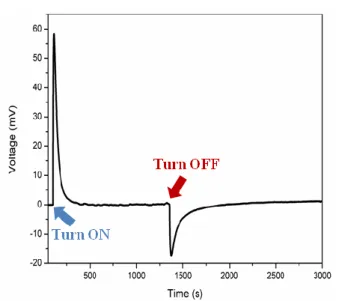
after reaching a peak point, this voltage buildup appears to diminish over time until it reaches a steady state in the presence of light illumination. At the steady state, when the light is switched off, a negative potential appears, which comes back to the initial point after short time. The observed operational mechanism of the LS-NS device is based on the photovoltage buildup rather than the immediate charge collection. This operation does not require external biasing. To understand the working of the device, it is worth mentioning that the non-trapped charges, which are held capacitively across the LS-NS device, are the stored charges, continuously decaying because of the shunt resistor with the RC decay of the whole circuitry (device + shunt resistor). There exist also trapped charges, beside the exponentially decaying stored ones. Simultaneously, the external circuitry tends to neutralize the trapped charges in the NCs for eventually obtaining charge neutrality across the device. With light impinging on the device, the transient response reaches a peak, at which these opposing components become equal to each other and balance each other. The net photovoltage buildup appears to decay after this point. The decay continues until the steady state is reached. By switching off the light at this steady state level (see Figure 4.2.1), the net potential goes negative. This is the potential of the trapped electrons.
Figure 4.2.1 Changes in the voltage buildup in time via switching the incident light on and off (with 0.153 mW/cm2 at 350 nm), marked with respective blue and red arrows.
While the light is on, some of the trapped charges draw holes from the Al contact to ensure the neutral state of the device. At the point when light is turned off, since there are no accumulated holes on the Al anymore, the net voltage reaches the lowest negative level and starts to recover and goes back to the zero level. This behavior shows the effect of trapped charges inside the NCs and the time taken to sweep out these charges. This indicates that the LS-NS device has a memory effect (within a certain time window).
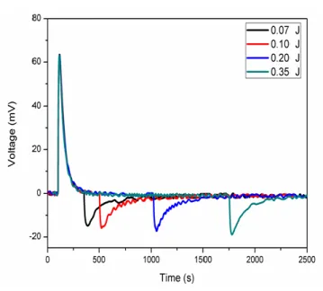
As another interesting feature, LS-NS devices can also be used to give information directly about the total amount of incident light power impinging on the device within a certain exposure period of time. This corresponds to the total incident optical energy to which LS-NS has been exposed. We found that the magnitude of the negative voltage appearing after switching the light off, which is directly proportional to the number of trapped electrons inside the NCs, change accordingly in response to changing light exposure time. This is due to proportional photocharging during the period of light exposure as seen in Figure 4.2.2. However, this will work provided that the trap states in the NCs are not yet fully occupied and there are still more trap states available.
Figure 4.2.2 Effect of photocharge trapping inside the NCs as the incident light shines continuously on the nanocrystals skin for different periods of time at 350 nm (0.175 mW/cm2). Here the total of incident optical energy given in the legend is the amount of incident optical power multiplied by the exposure time and the exposure area.
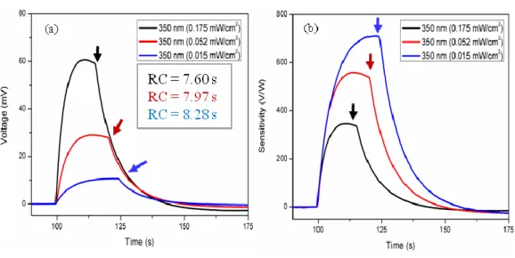
For a detailed understanding of the device operating principle, we further studied the LS-NS operation by systematically varying the excitation wavelength and illumination intensity. The voltage buildup variation in response to excitation with different intensities at different wavelengths is shown in Figure 4.2.3(a). We observed a higher voltage buildup at a shorter excitation wavelength, accompanied with a larger negative voltage after switching off the incident light. Due to the stronger optical absorption of CdTe NCs at shorter optical wavelengths, the voltage buildup is expected to increase with decreasing excitation wavelength. Essentially, this is because there are more electron and hole states available in a NC at a larger energy. This implies that a NC can absorb a larger number of photons at higher photon energies (i.e., at shorter wavelengths), photogenerating more electrons and holes under optical illumination at the same intensity level compared to longer wavelength excitation. This is in strong agreement with the profile of optical absorption spectrum of CdTe NCs.
We also observed that the device exhibits a larger negative voltage at a shorter excitation wavelength due to the increased number of trapped charges, again owing to the increased optical absorption. It also takes more time to relax this increased number of charges in the absence of light as shown in Figure 4.2.3(a). Similarly, Bulović et al. reported a decreasing external quantum efficiency of their cycled devices (NC-LEDs) as a result of charging of the NCs by trapped electrons over time [68]. We can measure the trap charge density in our devices, using the negative voltage value and the time required to recover after the light exposure is stopped.
Next, a meaningful figure-of-merit has been formulated to evaluate photodetection sensitivity of our device. Here we used the generic definition of the sensitivity as the ratio of electrical output signal to the optical input signal. Adapting this definition for the LS-NS devices, the photodetection sensitivity (S) is given by the ratio of photovoltage buildup to the incident optical power (i.e., S=V/P, where V is the photogenerated voltage (in V) and P is the optical power (in W) impinging on the device). Figure 4.2.3(b) presents the sensitivity of the LS-NS device as a function of the excitation wavelength, with an increasing trend towards shorter wavelengths in agreement with the discussions above.
Figure 4.2.3 (a) Variation of the voltage buildup at different excitation wavelengths and intensity levels. Light was turned off after reaching the peak point. (b) Corresponding sensitivity curve of the LS-NS device as a function of excitation wavelengths.
We also studied the effect of varying incident power on the voltage buildup at a fixed wavelength (in this case, 350 nm). We observed that, with increasing power, the photosensitivity decreases while the response time grows shorter. This is because of the decreased RC, which means a faster response time and a decreased level of sensitivity (Figure 4.2.4).
Figure 4.2.4 (a) Response time increases with the decreasing power since both deeper and shallower states saturate and (b) increasing illumination, resulting in decreased sensitivity because of filling the long-lived trap states. Arrows indicate the point in time when the light was turned off.
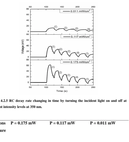
Furthermore, we observed that the RC decay kinetics changes over time in LS-NS devices (see Figure 4.2.5). While the shunt resistance (R) is fixed at 200 MΩ, the RC decay time constant decreases with time because of the change in the capacitance of the device. This change in the capacitance comes from the variation in the effective dielectric constant of the NC layer and thus the overall capacitance of the LS-NS device. The decreasing device capacitance can explain the reduced charge accumulation in the presence of light over time, which then results in a lower voltage buildup. Likewise, after reaching the peak point, the decrease in the device capacitance speeds up the RC decay, which is in correlation with the data summarized in Table 1.
![Figure 2.1.1 Energy levels of bulk materials which are mostly used in NCs synthesis [28]](https://thumb-eu.123doks.com/thumbv2/9libnet/5912114.122541/25.892.196.760.189.552/figure-energy-levels-bulk-materials-used-ncs-synthesis.webp)
![Figure 2.1.3 Device structure of ultrasensitive solution-cast quantum dot photodetector [19]](https://thumb-eu.123doks.com/thumbv2/9libnet/5912114.122541/27.892.283.676.719.1056/figure-device-structure-ultrasensitive-solution-cast-quantum-photodetector.webp)