LOW LOSS OPTICAL WAVEGUIDES AND
POLARIZATION SPLITTERS WITH
OXIDIZED AI,Ga,^ As LAYERS
A THESIS
SUBMITTED TO THE DEPARTMENT OF PHYSICS
AND THE INSTITUTE OF ENGINEERING AND SGIENCt
OF BILKENT UNIVERSITY
IN PARTIAL FULFILLMENT OF THE REQUIREMENTS
FOR THE DEGREE OF
MASTEi OF SCIENCE
Alpan BeL
jf i 0 s e
OXIDIZED AlxGai_xAs LAYERS
A THESIS
SUBMITTED TO THE DEPARTMENT OF PHYSICS AND THE INSTITUTE OF ENGINEERING AND SCIENCE
OF BILKENT UNIVERSITY
IN PARTIAL FULFILLMENT OF THE REQUIREMENTS FOR THE DEGREE OF
MASTER OF SCIENCE
by
Alpan Bek
August 1998
Ы.С
& 4S
dissertation for the degree of Master of Science.
*
Prof. Atilla Ayqinh (Supervisor) I certify that 1 have read this thesis and that in my
opinion it is fully adequate, in scope and in quality, as a dissertation for the degree of Master of Science.
1
certify that1
have read this thesis and that in my opinion it is fully adequate, in scope and in quality, as adissertation for the degree of Master of Science.
Approved for the Institute of Engineering and Science:
Prof. Mehmet B a r a ^
Abstract
LOW LOSS OPTICAL WAVEGUIDES AND
POLARIZATION SPLITTERS W ITH OXIDIZED
Al^Gai_xAs LAYERS
Alpan Bek
M. S. in Physics
Supervisor: Prof. Atilla Aydınlı
August 1998
Low propagation loss waveguides, operating at 1.55 fim optical wavelength, are fabricated utilizing oxidized AhGai_a;As layers. MBE grown multilayer semiconductor heterostructures are characterized before and after oxidation by ellipsometric techniques. In fabrication of optical waveguides, reactive ion etching method is used extensively. Loss measurements are performed, involving a fiber input-coupled laser source setup using Fabry-Perot resonance technique. Propagation loss of an AlGaAs based multilayer rib waveguide with oxidized A h G a i_
3
,As top layer is observed to reduce from6
d B /cm to as low as 1 clB/cm lor TM and from 3.7 dB /cm to as low as0.6
d B /cm for TE polarizations in the presence of metal electrodes on top of the rib. These results arc compared with loss measurements on standard rib waveguides. Polarization splitters are also fabricated with the same material. Effect of the oxide layer on the polarization splitter’s coupling length for TE and TM polarizations are measured. Polarization extinction ratios as high as 12.4 dB are obtained. Polarization extinction ratios are also attempted to be controlled by the use of electro-optic effect inK e y w o r d s : Optical loss, waveguide, coupler, oxidation, reactive ion etching, ellipsometry, Fabry-Perot, polarization splitter
özet
AlxGaı_xAs TABAKALARIN OKSİTLENMESİYLE
GELİŞTİRİLEN DÜŞÜK KAYIPLI OPTİK DALGA
KILAVUZLARI VE KUTUPLULUK AYRAÇLARI
Alpan Bek
Fizik Yüksek Lisans
Tez Yöneticisi: Prof. Atilla Aydınlı
Ağustos 1998
Al.T;Gaı_T;As tabakaların oksitlenmesi metoduyla 1.55 dalgaboyunda çalışan, düşük optik kayıplı dalga-kılavuzlan üretildi. Üretimde kullanılan MBE ile büyütülmüş çok tabakalı hetero-yapıların oksitlenmeden önceki ve sonraki özellikleri elipsometrik yöntemlerle ölçüldü. Optik dalga-kılavuzlarmm üretim aşamasında, büyük ölçüde etkin iyon aşındırıcıdan yararlanıldı. Optik kayıp değerleri, optik-lif çiftleyicili lazer kaynağı kullanılan bir deney düzeneğiyle Fabry- Perot çınlamaları gözlemlenerek bulundu. Metal elektrotla kaplı, oksitlenmiş ALGaı_j;As üst tabakalı AlGaAs çok tabaka tabanlı bir optik dalga-kılavuzunda optik kaybın; TM kutuplu optik alanlar için
6
dB /cm değerinden1
d B /cm , TE kutuplu optik alanlar için .3.7 d B /cm değerinden 0.6 d B /cm kadar düşük değerlere indiği saptandı. Bu sonuçlar standart yapıdaki dalga kılavuzlarının kayıp ölçümlerinden elde edilenlerle karşılaştırıldı. Aynı malzeme ile kutupluluk ayırıcılar da üretildi. Oksit tabakanın TE ve TM kutupları için çiftlenme uzunluğu üzerindeki etkileri ölçüldü. 12.4 dB kadar yüksek sönüm oranları elde edildi. Elektro-optik etki sayesinde kutupluluk ayrım uzunlukları voltajA n a h ta r
sö z cü k le r: Optik kayıp, dalga-kılavuzu, çiftleyici, oksitlenme, etkin iyon aşındırma, elipsometre, Fabry-Perot, kutupluluk ayırıcı
Acknowledgement
I would like to express my deepest gratitude to Prof. Atilla Aydınlı for his supervision in research, encouragement, understanding, and friendship throughout the entire work. My special thanks go to Prof. Nadir Dağlı for supplying financial aid for laboratory facilities, helpful suggestions on many aspects of this work and hospitality. I also would like to thank Prof. Ekinel Ozbay for providing necessary motivation during the early periods of this project. My thanks go to Prof. Cemal Yalabık for providing moral support and obtaining financial support for my travel abroad.
I would like to address my thanks to Baki Açıkel for his help in fabrication. Dr. Y. T. Byun for his help in wet etch characterization and measurements, and Dr. Andrea Fiore, Dr. Ali Shakouri, Dr. Ceyhun Bulutay and Cern Oztiirk for the fruitful discussions on various subjects and computational aid. I also would like to thank Mr. James Champlain and Mr. Ryan Naone for the MBE growth of the structures.
Many thanks to my dear friends Koray Atasoy, Erol Sağol, Arikan Açar, Ersin Keçecioğlu, Kaan Güven, Mete Atatüre, Hakan Fenderya, and Burak Temelkuran for being who they are and meaning what they mean to me.
It is my pleasure to dedicate this work to the warmest love of my family and to the lovely memory of my grandmother...
This work is supported by a NATO CRG grant and NSF Division of International Programs.
Abstract i
Özet i
Acknowledgement i
Contents i
List of Figures iii
List of Tables vi
1 Introduction 1
1.1
Optical Integrated C ircu its... 11.2 Reducing Excess Propagation Loss and its A pp lica tion s... 3
2 Theory and Design 5
2.1
Single Mode Waveguide ... 52.2
Multilayer Waveguide S tru ctu re... 142.3 Optical L o s s ... 20
2.3.1 Loss M ech an ism s...
21
2
.3.2
Loss Characterization T ech n iqu es... 232.3.3 Simulations of Loss Due to Metal O v e r la y e r ... 25
2.4 Low Loss Waveguide D e s ig n ... 28
3 Fabrication 41
3.1 Epitaxial G r o w t h ... 41
3.2 Sample Cleaning ... 42
3.3 P h otolith ograph y... 42
3.4 Wet E tch in g ... 43
3.5 Reactive Ion Etching (RIE) ... 46
3.6 Oxidation of Al
0
.98
Ga0
.02
A s ... 563.7 Metal D e p o s itio n ... 56
3.8 L ift -o ff... 58
4 Characterization and Measurements 60 4.1 Characterization ... . ... 60
4.1.1 Spectroscopic Ellipsom etry... 60
4.1.2 Oxide Characterization... 64
4.1.3 RIE Depth P r o f i l i n g ... 69
4.2 M easurements... 70
4.2.1 Optical Propagation Loss M easurem ents... 70
4.2.2 Characterization of Polarization S plitters... 77
4.2.3 AC and DC Bias M easurem ents... 82
5 Conclusions 85
2.1 The Slab W a v e g u id e ... 6
2.2 The Symmetric Slab Waveguide Modes ... 9
2.3 The Rib W aveguide... 12
2.4 The Effective Index Calculation Steps . ... 12
2.5 Field Distribution of Zeroth and First Order Modes in the ?/-direction 13 2.6 Dependence of Confinement on Rib W i d t h ... 14
2.7 The Four Layer Rib W a v e g u id e ... 15
2.8 Confinement of the Optical Field Under the R i b ... 16
2.9 Metal Coated Four Layer Rib W avegu ide... 17
2.10 Dependence of Refractive Index on Aluminum Composition (a;) of AlxGa\-xAs at A = 1.55 ¡ i m ... 17
2.11 Alx:Ga\-xAs! AlyG ai-yAs M ultilayers... 18
2.12 Single Mode AlGaAs Rib W a v e g u id e ... 19
2.13 Mode Calculation with B P M ... 20
2.14 The Vertical Field Distribution in the Absence of a Metal Layer . 26 2.15 The Vertical Field Distribution in the Presence of a Metal Layer . 27 2.16 Calculated Loss as a Function of Top Cladding Thickness... 27
2.17 Loss Calculation-1 28 2.18 Loss Calculation-2 ... 30
2.19 Final Design of W G l Waveguide... 31
2.20 Final Design of WG2 Waveguide... 31
2.21 Final Design of WG3 W aveguide... -. . . 32
2.22
2.23 2.24 2.25 2.26 2.27 2.28 2.29 2.30 3.1 3.2 3.3 3.4 3.5 3.6 3.7 3.8 3.9 3.10 3.11 3.12 3.13 3.14 3.15 3.16 3.17 3.18 3.19 3.20 3.21Electic Field Distribution of the Odd and Even Modes of a
Polarization Splitter ... 33
Waveguide Coupler Polarization S p l i t t e r ... 34
Coupling Ratio versus Core Layer Thickness... 35
Coupling Ratio versus Rib W i d t h ... 36
Coupling Ratio versus Top Cladding Thickness dt as in Fig. 2.12 . 36 Coupling Ratio versus A n ... 37
Multiple Coupling of TE Mode between the two Waveguides . . . 38
Coupling of TE Polarized L i g h t ... 39
Coupling of TM Polarized L ig h t ... 40
Wet Etched Surface of AlAs Crystal in Citric Acid Solution . . . 45
Wet Etched Surface of AlAs Crystal in Hydrochloric Acid Solution 45 Wet Etched Surface of AlAs Crystal in Phosphoric Acid Solution . 45 Components of RIE S y s t e m ... 47
Photoresist Loss during the Etch Rounded Photoresist P r o f ile ... Penetration of Energetic Ions Wriggled S id e w a lls ... Photoresist Covered with Ti prior to RIE of the Rib 48 48 Sputtered Photoresist... 49 49 49 50 Grass Formation ... 51 Rough Etched S u r f a c e ... 51
Polymer Deposition during R I E ... 52
RIE Etched Waveguide P ro file ... 53
RIE Etched Waveguide S id e w a lls ... 53
Simulation of RIE Interference Pattern for W G l ... 54
Simulation of RIE Interference Pattern for W G 3 ... 54
Monitored RIE Interference Pattern for WG3 55 Photoresist Profile I ... 57
Photoresist Profile I I ... 57
E-beam E vaporator... 58
4.2 Ellipsometric Measurement of the AlAs W a f e r ... 63
4.3 Ellipsometric Measurement of the Thick Top-cladding Wafer . . . 64
4.4 Microscope View of AlAs Wafer Edge Oxidized for 20 Minutes . .
66
4.5 Microscope View of AlAs Wafer Edge Oxidized for 60 Minutes . .
66
4.6 Lateral Oxidation Depth versus T i m e ... 67
4.7 Refractive Index of Oxidized A lA s ...
68
4.8 The Zeroth Order Mode of AlAs W a v e g u id e ... 72
4.9 The First Order Mode of AlAs W a v e g u id e ... 72
4.10 Loss Measurement S e t u p ... 73
4.11 Single Mode Waveguide Fabry-Perot Resonances . ... 74
4.12
Double Mode Waveguide Fabry-Perot R e so n a n ce s... 744.13 SEM Picture of a BOB Covered Al
0
.98
Ga0
.02
As Waveguide Rib . . 754.14 The Loss Coefficients and Facet Reflectivities of W G l and WG2 W a v e g u id e s ... 76
4.15 The Loss Coefficient and Facet Reflectivity of WG3 Waveguides . 77 4.16 Optical Field Output at the Left Output P o r t ... 79
4.17 Optical Field Half-and-half at Both Output P o r t s ... 79
4.18 Optical Field Output at the Right Output P o r t ... 79
4.19 Coupling Ratio of WG2 Polarization Splitter for gap = 3.00/im 80 4.20 Coupling Ratio of WG2 Polarization Splitter for gap = 3.25/zm 81 4.21 Coupling Lengths of WG2 Polarization S p litte rs... 82
4.22 TE Modulation at One Output Port of the Waveguide ... 84
List of Tables
4.1 4.2 4.3 4.4 4.5The Ellip.soinetric Data of W G l wafer 64
The Ellipsometric Data of WG3 wafer ... 65 Ellip.sometric Measured Thicknesses of A l A s ... 67 Cauchy Coeificients for AlOx ... 68 Coupling Length Ratios of WG2 Determined by Experiment,
Effective Index Method, and BPM 81
Introduction
The idea of optical signal transmission and processing has developed after a coherent light source, the laser, was developed at 1960’s. It was possible to transmit laser beams through the air, yet ineificiently, because of the unpredictable changes in ambient conditions. It was also possible to manipulate laser beams by the usual optical components such as lenses, prisms, and mirrors. Making use of such systems for practical purposes were e.\pensive and hardlj^ stable. The concept of integrated optics^”’^ emerged, replacing air with the waveguiding optical fibers and conventional electrical systems with the optical integrated circuits. The advantages of optical integrated circuits over electrical circuitry would be immunity from electromagnetic interference, freedom from electrical short circuits or ground loops, safety in combustive environment, security from monitoring, low-loss operation, low power consum])tion, improved reliability, large bandwidth, small size, and immunity to mechanical vibration.
1.1
Optical Integrated Circuits
Optical integrated circuits can be designed in two major forms. Hybrid integration forms'’ are composed of two or more different substrate materials bonded to each other to optimize performance of different devices. Monolithic integration of o])tical integrated circuits require an optically active material.
CHAPTER 1. INTRODUCTION
usually one of the following direct band-gap semiconductors like GaAs, AlGaAs, GaAsP, GalnAs and other III-IV and II-VI semiconductors. These materials offer plenty of applications in various aspects of integrated optics. High-speed low drive-voltage modulators^ and switches, are some of these. In optical devices, ternary and quaternary compounds are particularly useful because the refractive index of the material can be tuned by altering the relative compositions of elements.
Ever since the fiber-optic technology has come out with the development of high bandwidth, low-loss, single-mode fibers lor optical telecommuniccxtion, the need for suitable integrated optical element was born, to efficiently couple to the optical field from these fibers. Th(' evolution of rib, strip, and channel optical waveguides has began with the extensive studies of refractive index profile, waveguide dispersion, and propagation loss on Ti-diffused LiNbOs. However, since the monolithic integration was possible only on the optically active substrates, the studies have extended to the implementation of Alj;Gai_
3
;As/GaAs systems. The fact that Ala;Gai_3
;As fabrication technology is already well developed, makes its use advantageous. Also this system has a unique property that the lattice constants of GaAs and AlAs are very close (.5.654 and 5.660A
respectively'*^). Thus the layers of Al.,.Ga.i_„.As with greatly diflerent A1 concentrations can be epitaxially grown on top of each other with little strain. The possibility of light generation and detection in Afi-Gai-j As systems is another advantage. However, all the named advanta.ges of Al.,;Gai_;,;As systems were screened due to high insertion loss. Significant progress in fabrication techniques has reduced the effect of high insertion loss to tlie LiNbOs levels. The other difficulty in the use of AlGaAs substrate has been the propagation loss. While propagation loss due to scattering from imjxerfections in the as grown material and roughness introduced during fabrication process (such as sidewall roughness) have been minimized by superior growth and fabrication techniques, polarization dependent propagation loss due to presence of a lossy medium (such as a metal electrode) in close proximity of the propagating light has remained as a problem. Metal electrodes are almost always present as a lossy mediain active devices to make use of the bulk electro-optic effect.^ Furthermore, this loss turns out to be polarization dependent due to lower symmetry of the heterostructures as the device medium. TE and TM modes of propagation experience different boundary conditions in satisfying Maxwell’s equations, hence result in polarization dependent loss and polarization dc'pendent device operation. While polarization dependent optical loss due to metal electrodes has been used to fabricate various types of polarization dependent devices, it also caused a. major problem in the progress of polarization independent devices. Thus, in trying to achieve active devices with high speed operation, excess polarization dependent optical propagation loss becomes a major problem and needs a solution.
1.2
Reducing Excess Propagation Loss and its
Applications
A significant part of this work was devoted to reduce the metal electrode induced optical propagation loss for polarization independent device applications of AlGaAs based integrated optical circuits. We have followed two methodologies to achieve our goal.
One way to reduce the optical loss is to increase the semiconductor cladding layer thickness under the metal electrodes. Although application of this method results in significant reduction of the electrode loss, it also re<iuires excessive amount of epitaxial growth time, and excess applied voltage. Moreover, it causes planarization problems during fabrication.
Another possibilit}^ is to introduce a low ind(^x material under the metal electrode to effectively suppress the optical field befoix' it reaches the elec trode. Thus, oxidized Alj,Gai_a;As layers (AlOx) were introduced into A lyG ai-yA s/A lzG ai-jA s optical waveguides with metal electrodes.
Prior to fabrication and measurement of waveguides with AlOx layers, the index and thickness measurements of AlOx material were done by spectroscopic ellipsometry.
CHAFTER 1. INTRODUCTION
AlOx has I’ecently been used extensively in vertical cavity surface-emitting laser (VCSEL). Also, latest results in GaAs based iiietal-oxide-seiniconductor field effect transistor (MOSFET) with thin AlOx layers offer hope of applying voltage to active optical waveguide devices. Therefore, low-loss directional coupler polarization splitters are fabricated for characterization of the effects of the oxide layer in a polarization dependent device. The coupling ratios as a function of coupler gaps and polarization extinction ratios were measured. The coupling lengths of these splitters were determined from the measurement data. Both effective index calculations and simulations using a 3-D semi-vectorial finite difference algorithm were done which showed good agreement with the measured data. The application of DC bias to further tune the polarization extinction ratio was found to be ineffective. On the other hand, AC bias measurements resulted in a modest response from the coupler in a limited range of frequencies.
In the following chapters, tlie theory of waveguicling in semiconductor based substrate materials using effective index analysis is summarized. A model single mode waveguide design with the appropriate properties is estaljlished. The simulations of expected behavior of this model and expected behavior of application to polarization splitters, the detailed description of the fabrication steps, the measurement methods, measured loss reduction and polarization splitting results are presented.
Theory and Design
The basic idea of optical waveguides is to confine and propagate light in dielectrics or semiconductors, as opposed to free space opticsT^ 'fliis can be managed b,y handling light in properly designed geometries of semiconductor (multilayer in general) structures. Propagation of light is not unique in a cavity, but varies with polarization and spatial distribution of the field components due to geometry and refractive index of the media. At a given wavelength, an optical waveguide may support one or more modes of light. Single mode o])eration and low propagation loss are the main characteristics of waveguides, tliat are desired for most of the active and passive waveguide applications in photonic integrated circuits (PIC). Therefore, the determination of parameters to assure these properties in guided wave optics becomes essential. Our design is based on the calculations of the necessary conditions for single mode operation Iry the use of effective index approach in waveguide theory.
2.1
Single Mode Waveguide
The principles that govern the behavior of light in optical waveguides, stem from well-known Maxwell’s equations under appropriate boundary conditions.
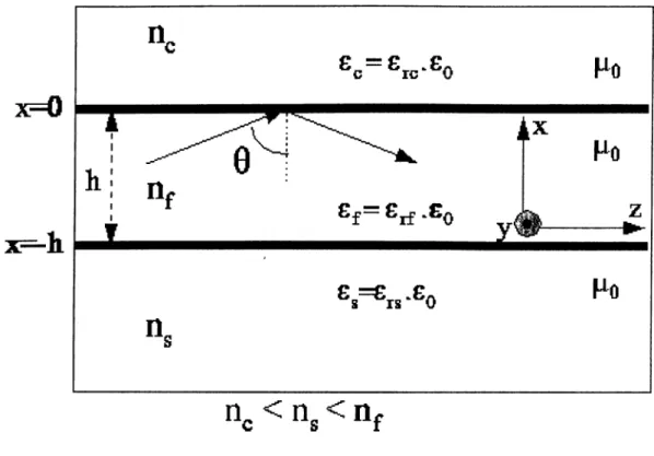
As an example, let us consider a structure that is composed of three different layers, stacked together on top of each other, such that the middle layer has the
highest refractive index, and the most of the field intensity is confined in the middle (core) layer due to total internal reflections. In this geometry, the top layer is called the cladding and the bottom layer is called the substrate. This structure is called a slab waveguide.
CHAPTER 2. THEORY AND DESIGN 6
Figure 2.1: The Slab Waveguide
Maxwell’s Equations for isotropic, lossless, dielecti’ic medium are,
V X £ = - , . 6 ^ V X H = eoH ——
(H (2.1)
where Cq and /¿o are the dielectric permittivity and magnetic permeability of the free space resj^ectively and n is the refractive index of the medium. The scalar wave equation for the field then turns out to be
where represents any of the field components E or / / . Choosing s-direction as the propagation direction of the field, one can denote the electromagnetic field as
E = E {x ,y )e II = H \ x ,y )t (2.3)
[5 representing the propagation constant in .^-direction and u> representing the
angular frequency w = Here, A is the wavelength of the field and c = is the speed of light in free space. One should note that in all regions.
/HO ^0
propagation constant fl is the same due to phase matching condition and the fields are independent of y due to symmetry along ?/-direction. Keeping that in mind, we can substitute these forms of field into Ecjs. 2.3. The operators ^ and ^ then become equivalent to iuj, —ill and 0 respectively. There conies the striking fact that Eqs. 2.1 yield two modes of electromagnetic field with mutually orthogonal polarizations. The one with the field comjjonents Ey, H^ and 7T is called the TE mode and the oneiwith the field components Ej., IIy and E- is Ccdled the TM mode. The reason we refer to two different sets of field components is that, their wave equations, are coupled to each other within the same set, while they are totally indej^endent of the other set’s variables :
dx'^ + {koiif - II )Ey = 0 Hj, = 0 Ey IL = - - 1 d i e ^ + (k^n] - (T^)IIy = 0 E , = OJf.10 iiOflo dx HHy p 1 OH, ioconl iojcoul Ox (2.4) (2.5)
The scalar wave equation for Ey gives us a clue about tlie form of field component
Ey·.
d'^E, ^ d^Ey
+ kln^Ey = 0
dx"^ dz'^
A,ssuming E y (x ,z ) — A h{kx,x)h{kz,z)^ where h is a harmonic function like and a is an arbitrary propagation constant, then the general form of Ey becomes.
CHAPTER 2. THEORY AND DESIGN E.„ =
Ey =
a· > 0 - h < X < 0 (2.6) .y - ^ X < - hwhere = k^j = k-zs = clue to phase matching boundary conditions as mentioned before. Putting this form into Eq. 2.4 we obtain a set of equations relating ai to ni as follows ;
—al + l3‘^ — k-QU^
- q;2 + fl^ = kin] By the same procedure we can find to be;
(2.7) IL
=
X >0
■' tJfJ.0 ^ ' - h < X <0
I J -i u n o;r <
- h (2
.8
)and imposing the necessary boundary conditions we can ol)tain the eigenvalue equation ;
tan kz'h — etc + eVs (2.9)
(i
“¿r)
Remembering that, until here, we ha.ve made use of only the first set of comiDonents for TE polarization, we can extend this approach to the second set of field components for TM polarization and obtain yet another eigenvalue ec[uation as follows : tan kxli = n^f (V n? n ILSii n. -L9Ls. n\ kx ' kx 1_ 71^ kx iLOijLnl kx (2.10)
Now, we have all the necessary parameters to determine the number of modes that a slab waveguide can support. For this, let us investigate two possible geometrical configurations. First, let us take a symmetric slab guide such that and
— as = a. Taking the sign of the field in the substrate to be negative for odd
(sine) modes and positive for even (cosine) modes, the eigenvalue equations for TE and TM modes become :
tan k,-h\ * ( f · * k'x for ev(?ii modes
— ^ for odd modes
and
(2.11)
tan kx h \na J kxT~ foi' even modes (2.12)
_ ^ modes
t
V«/ / «
respectively. Using the Eqs. 2.7 and 2.9 for TE polarization, we finally arrive at the most significant relation in determination of numlDer of modes as.
kxh
, 2 7 ■' V 2 / 4
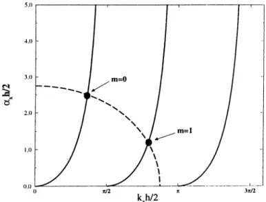
The number of guided modes in the symmetric slab vuiveguide, depends on the quantity on the right-hand side of Eq. 2.13.
Figure 2.2: The Symmetric Slab Waveguide Modes
The circle in figure 2.2 shows this quantity, where the other curves are the solutions of the eigenvalue equation. The curves starting from 0 and the integer
CHAPTER 2. THEORY AND DESIGN 10
multiples of tt represent the symmetric modes where the curves starting from half integer multiples of tt represent the antisymmetric modes. The modes that a certain symmetric slab can support, are the modes that the circle intersects as in the Fig. 2.2.
The propagation constants of guided modes lie in the interval koiis < jl <
koUf. If we normalize /1 to ko, then we have the relation < n „jj < ??./,
where n^jj = This index is called the effective index. The guided modes’ propagation constants behave as if they were propagating in a. medium, having refractive indices ecpial to their effective indices. Having developed the necessary relations for a symmetric slab waveguides, we can generalize this formalism to
asymmetric slab waveguides as well. For this aim, an asymmetry parameter is
defined.
n:
n!
a =n] - 77.2 (2.14)
such that this parameter takes values.
a = (2.15)
nor
0 for symmetric slab waveguides . 0 < a < oo for asymmetric slab waveguides
For the numerical calculation purposes, it is beneficial to introduce the rrnalized thickness V and guide index h as follows.
V = kohyjnj -
772
(2.16) andb = n e f P - nl
Uf — ni
'/
(2.17)so as to get to the normalized eigenvalue equation for TE polarization :
Vs/l — h = tan ^ \ j \ f + tan ’ h + mir (2.18) 1 - i i V 1
by the use of Eqs. 2.9, 2.14, 2.16 and 2.17. The normalized eigenvalue equation for TM polarization can be found by following the same kind of analysis :
v V i - b
c — a 1 1 - b+ rnir (2.19) where c is defined cVS c = In Eqs. 2.18 and 2.19, ni denotes an integer corresj^onding to the mode order and comes as a natural consequence of the periodicity of the normalized eigenvalue equations.
The generalization of the preceding mode calculations to i-D geometries is called the effective index method. Let us investigate the following waveguide structure, which is called a rib waveguide (Fig. 2.3). While the material index profile in the vertical direction provides vertical confinement, the rib etched into the top Iciyer breaks lateral symmetry and introduces horizontal confinement due to an effective index experienced by the field.
The effective index method calculates this effective index experienced by the propagating light by first dividing the rib waveguide geometry vertically along the symmetry lines (Fig. 2.3). Then the effective index of the resulting slab waveguides are solved. The resulting effective indices for the slab waveguides, then form a 3 layer slab waveguide, whose effective index is the desired result. Effective indices for TE and TM modes are calculated separately as they satisfy different boundary conditions. If the TM (TE) effective index is desired, one calculates the TM (TE ) effective in the first step and then uses thc'se effective indices in forming the final slab waveguide structure l)ut solves for the TEl(TM) set of equations (Fig. 2.4).
After having calculated the effective indices, the single mode conditions for symmetric and asjmimetric geometries can be stated as :
0 < fo < 7T for symmetric waveguides
tan~^(^/a) < E < tan~^(x/a) + x for asymmetric waveguides (2.20)
The field distribution of the guided modes in rib waveguides differ from the slab waveguides. The lateral confinement of the light, due to the physical step of the rib results the propagation of light possible only in .^-direction and the
CHAPTER 2. THEORY AND DESIGN 12
Figure 2.3: The Rib Waveguide
-I I “ C
ns I
i
II
i ins III
1 1
\
______ 1 1
. 1 1____
neffl
neffll
nefflll
1--- 1
n e ffl n e ffll n e fflll
0
neffL ... ... J
TM (TE) Equations
TE (TM) Equations c=> n.
TM(TE)P’igure 2.4: The Effective Index (Jalculatioii Stcp,s
maximum intensity of field lies just under the rib. The waveguide structures, that do not obey the conditions of Eq. 2.20, may not support any propagating modes or support more than one mode. In the first case, the waveguide does not support any modes, meaning that light radiates out of the waveguide, where
in the second case, supports more than one mode and is called a multimode Wciveguide. The proj)a.gating modes of light in those waveguides start from the zeroth order (???. — 0, T Eq or T Mq) mode and continue to first, second order
modes (m = 1 : TT'i, TM\ ; m = 2 : TE-2^ TM^) and so on. A demonstration of
this situation is given in Fig. 2.5.
Figure 2.5: Field Distribution of Zeroth and First Order Modes in the y-direction
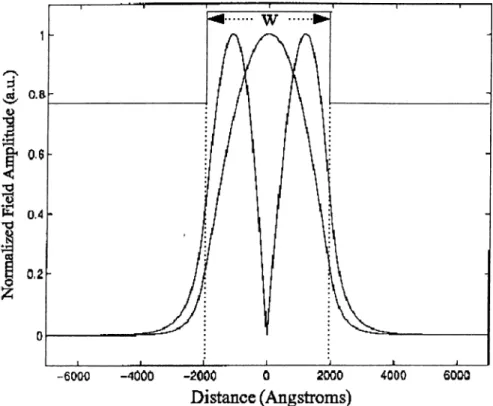
There is yet another property concerning the confinement of the optical mode in the waveguide. The confinement strongly depends on f.he parameter to (width of the rib). This effect is demonstrated in Fig. 2.6. The full width half maximum (FVVHM) of the field intensity narrows down, as a consequence of increasing width of the rib. Hence the confinement factor is larger in the sharper peaks.
CHAPTER 2. THEORY AND DESIGN 14
-2 -1.5 -1 -0.6 0 0.6
Distance (|im)
1.6
Figure 2.6: Dependence of Confinement on Rib Width FWHM of first order modes in y-direction narrow as w decreases.
2.2
Multilayer Waveguide Structure
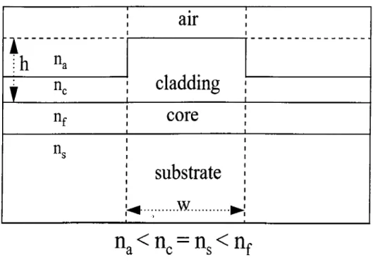
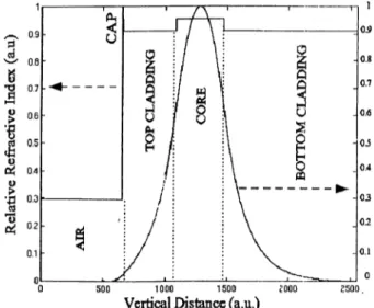
In the fabrication of three layer rib waveguides, generally the top cladding layer is taken to be the air. This makes a sharp index step. Therefore most of the mode field is expanded into the rib itself. However, as the light is confined to the top layer below air, the field extending to the surface exp(:'riences loss due to surface roughness as well as loss due to strong interaction with a.ny nearby lossy medium such as a metal electrode. Because of this reason, it is preferable to develop a more sophisticated structure. A four layer rib waveguide gives the advantage of minimizing loss of optical field, while the mathematical ibrmulations are very similar to the three layer rib waveguide analysis. Fig. 2.7 sketches a four la.yer rib waveguide with the uppermost cladding layer being the air. Fig. 2.8 demonstrates schematically how the field is distributed in the rib waveguide structure.
air
n„
n . nrn.
cladding
core
substrate
... w ... n a < « c = n s < n fFigure 2.7: The Four Layer Rib Waveguide
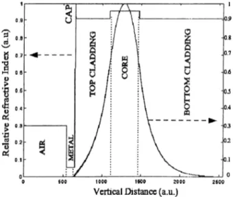
The top cladding inti’oduced above the core allow.'i for space for the opticcd field to quench further before significant optical power reaches to the air interface resulting in a structure less susceptible to surface loss mechanisms.^“ As active devices require metal electrodes in the vicinity of the optical field to control the device electrically through the electro-o[)tic effect, the four layer structure ¡:>rovides a further advantage for metal electrode induced loss, keeping in mind that metals have large absorption in the wavelengths of the interest for telecommunication. Most of the photonic integrated circuits are designed to operate at the wavelengths of fiber-optic communication for compatil)ility. These wavelengths are chosen to be 1.3 (.im and 1.55 /cm for maintaining minimum dispersion and minimum loss, respectively. A major aim in this work is to develop a method to prevent the metal induced loss in a imAal coated rib waveguide structure as in Fig. 2.9.
CHAPTER 2. THEORY AND DESIGN 16
Figure 2.8: Confinement of the Optical Field Under the Rib
The final heterostructure used for the design and fabrication of single mode waveguide is composed of alternating layers of AlGaAs. It is well known that addition of A1 lowers the index of refraction and hence control of composition allows for precise control of the refractive index^^ (Fig. 2.10). Since commercially available substrates are GaAs, which has the highest refractive index in the AlGaAs system, it becomes necessary to introduce a bottom cladding with a refractive index lower than the confining core layer but thick enough to quench the optical field before it reaches the substrate (Fig. 2.11).
As seen in Fig. 2.10, the index value decreases as the composition ratio of A1 increases. So, the core region A1 composition y has to be smaller tlum x in
"c .·
I I
1 1 1 * 11\ \
7 T"1
1\
T T /I I
I V 1 1 .... j·.-... -....1 ^ ^ : \ ' 1 1 V \ 'a '' ' ' ' V'■■■■:}
i
T··· o p tic a l fie ldFigure 2.9: Metal Coated Four Layer Rib Waveguide
Figure 2.10: Dependence of Refractive Index on Aluminum Composition (.r) of
Alj;Gai^xAs at A = 1.55 /tm
Fig. 2.11 to have an adequately higher index and so as to confine the optical mode vertically. The necessary values of x and n are cliosen to be :
X = 0.61 nAio.e1Gao.39As = 3.225
CHAPTER 2. THEORY AND DESIGN 18
Air
top cladding A lj G a p ^ A s core A ly O s j^ y A s
bottom cladding A ljG a i.^ A s
SI GaAs Substrate
. . . . . . 1 . . . .
F ig u r e 2. 11: AlxGai-xAsjAlyGoi _ / I s M u ltiIc iy e r s
Next step is to confine the optical field laterally. This is managed by etching the top cladding layer, to construct a rib shape with width to and height h. Using effective index calculations, we determined that.
core thickness dc = 0.7¡.im
bottom cladding thickness = ‘2.0j.im top cladding thickness in regions I and III dtc — 0.3/n??.
rib height h = 0.5//m
rib width 10 = 4.0f.im
would satisfy single mode operation at A = 1.55 /¿??? (Fig.
2
.12
).Since our object was to investigate the loss characteristics of such a waveguide with metal overlayer, the single mode operation was essential. Waveguide characteristics can also be calculated using numerical algorithms to solve the scalar wave equation with general n = n{x,y.,z). Such metliods are called Beam
Propagation Methods^‘^~^^ (BPM ). In this work, a commercial BPM simulator
was occasionally used to confirm various waveguide properties such as the mode spectrum and shape. BPM assumes small index differences along propagation
}
4
h=0.5|im dj=0.3|im i d=0.7|im4
d^=2.0iim au ^ w=4.0(imAlo.soGao 7
qA
s A1o.61^%39As n=1.0 n=3.072 n=3.225 n=3.072SI GaAs Substrate
Figure
2
.12
: Single Mode AlGaAs Rilr Waveguidedirection and no back reflected waves in waveguide. Under these conditions Eq. 2.3 reduces to :
dlj) ^ ^ '0 , 2 r 2t \ 21 /
•hkonr-^ = _ + _ + k^[n (a·, y, z) - (2.21)
where Ur stands for a refractive index describing the a.verage phase velocity of the wave. Numerical calculation with this method works reasonably for ir-invariant waveguides, as in our design, if the x and y axes are divided into sulFiciently small grid size with respect to axis grid size.
In Fig. 2.13, parameter Ubar stands for the computed index for the zeroth order mode and stands for the effective index, computed by BPM. In this graph, i/-axis shows the ratio,of optical power distribution over index to the total power. The sharp and intense peak at Ue/f — Ubar =
0
is the signature of a single mode waveguide. The other small peaks are due to virtual localization of the optical field at the index step boundaries, as a result of finite grid size, and are insignificant. As a result, BPM computations also yield single mode operation.CHAPTER 2. THEORY AND DESIGN 20
2.3
Optical Loss
The waveguide parameters such as widths and thicknesses can be calculated to reflect the demands of a particular design. But the non-ideal material properties and processing imperfections also affect the performance of tlie waveguides. An outstanding effect of these is the optical intensity attenuation of the mode as it propagates along the waveguide due to waveguide optical loss.^^’^·^ Letting Iq to be the initial intensity, optical intensity has to be a function of being the propagation direction, such that I{z) — Ioe~°" where cv is the loss factor, or e.xtinction coefficient, with units [ci??.“ ^]. Optical loss itself is often measured in units of dB /cm , where we define dB as the ratio of the transmitted to incident intensity (or power).
(IB = 10 log( ) in terms of intensity
(IB ■
20
l o g ( % ^ ) in terms of power^ lineUsing the definition of dB, dB loss and loss factor can be related ci,s,
(
2
.22
)OidB = 10
hüÖ-a (2.23)
where « ¿ s has units of dB /cm and a has units of cm. h The total loss factor is simply the superposition of optical losses from a number of sources.
2.3.1 Loss Mechanisms
Band-Edge Absorption Loss
The photons having energy close to the band-gap of the semiconductor, i.e, the energy difference between the valence and conduction bands, may be absorbed promoting an electron from the valence band to the conduction band. Absorption increases drastically, as the energy of the propagating photon approaches the band-gap energy of the material. The fundamental lower wavelength limit for the light propagation in semiconductor materials is therefore a natural consequence of band-edge absorption. Moreover due to existence of band-tails the operating wavelength of the low-loss waveguides should be well isolated from the band- edges. The operating wavelength of 1.55 ¡.tm satisfies this condition well.
Free-Carrier Absorption Loss
The absorption of carriers within the same band can also be significant as a loss component. The electrons (holes) can gain a higher energy level in the same band by absorbing a photon. It is predictable that, this kind of absorption increases as the electron (hole) concentration and photon wavelength increases, hree-carrier absorption is formulated as;
exfc = q^Xln^
CHAPTER 2. THEORY AND DESIGN 9,9
where Ue is the electron density, q is the electron charge, to i·'’ Ihe permittivity oi the free space, ¡.i is the mobility, m* is the effective mass of electron, c is the s])eed of light, no is the refractive index of the material vvitliout the free carriers and Ao is the wavelength. This kind of loss mechanism becomes significcuit at high doping concentrations. For demonstration it will be adequate to quote that a doping of
10
^® cm~^ yields a free-carrier absorption toss on the order of1
clB¡cm in GaAs. The use of undoped layers makes this mechiinism negligible in our waveguide.Scattering Loss
Any kind of roughness or disorder in the waveguide;, possibly created while growth and/or processing, lead to optical loss due to scattering. When the guided mode is distorted by an irregular change in refractive index, it may result in some portion of the guided mode to scatter out of the waveguide. This may even cause the optical field to couple to the higher order modes or to leak into the slab. The MBE and MOCVD layer growth techniques in semiconductors yield vertical boundaries flat within a monolayer of material, so that scattering in the ciystal plane is usually negligible. Lateral boundaries that are made up of etclied rib and ridge geometries, may be very problematic due to sidewall roughnesses serving as scattering centers. Optimization of wet or dry etching is required to minimize this loss component.
Radiation Loss
Radiation implies the leakage of energy from the guided mode either into the substrate or into the air above the waveguide. For well-designed Wevveguides, radiation loss is not an issue; nevertheless in some cases it becomes inevitable. The waveguides having sharp bends and curved sections also play role in high radiative loss. The curvature of any deviation from ’:-direction has to bexarefully designed in order to reduce the radiation loss. The bottom cladding thickness of 2 ¡.Lin is large enough to minimize radiation loss to Sf GaAs substrate.
2.3.2 Loss Characterization Techniques
We had previously stated the importance of loss reduction in our design. So we need the methods to measure the waveguide optical loss to demonstrate that quantitatively. For this reason the methodology of loss measurement techniques are presented in the following sections. There are two main approaches to measure optical loss called the cut-back technique and the Fabry-Perot re.sonance technique.
Cut-back Technique
This is the simplest approach to measure the optical loss in a waveguide. If we measure the amount of transmitted light through a set of identical waveguides having different lengths with a constant input power, we can deduce the loss coefficient. To guarantee the identical wa.veguides we can start with an initially relatively long waveguide and measure its transmitted optical intensity. Then, we cut a small slice from the end of the waveguide wafer and measure the transmitted light intensity again. Repeating this many times we can obtain the transmitted light intensity versus waveguide length curve, hence the name cut-back.
For the output intensities R and
/2
measured for waveguide lengths L\ andL2 the loss of the waveguide can be expressed as
1
where L\ is taken to be the longer waveguide length. For a. more precise result, output intensity has to be measured for a number of different waveguide lengths and \n(Iouillin) has to be plotted as a function of L. The resulting linear plot then yields a slope of —a.
Although the method is quite simple, its accuracy is questionable since the reproducibility of input coupling can hardly be guaranteed experimentally. Moreover in low-loss waveguides it may not be possible to distinguish the intensity change for a small change of waveguide length.
CHAPTER 2. THEORY AND DF^SIGN 24
Fabry-Perot Resonance Technique
Waveguides having miiTor like input and outjjut facets Ccui l)e regarded as waveguide cavities, thus resonators. The transmission tlirough this resonator is then a function of the loss in between the mirrors. Therefore the input cuid output facets of the waveguide has to be good cpiality cleaved facets.
The ratio of transmitted optical intensity (It) to the incident optical intensity
(li) can be written in terms of amplitudes, h
h
A ;A t A lA i
\ — Re \ — Re (1 - Re-^^Y 1 - Re^^e-°^^ 1 - Re-^^e~°‘^
(1 —
R e ~ " ^ Y+ 4/ie“"^sin“
(2.2.5) where R is the facet reflectance, o- is the loss coefficient, L is the cavity length and
S is the phase difference between adjacent waves iii the resonator. The maximum
transmission =
1
takes place when =0
and minimum transmission takes place when 6 = tt of the value,(1 - Re~<^^Y
lo (1 - Re~^‘^Y + 4/ÏC-"''- We can then define a. dimensionless contrast ratio k. as
(2.26)
(1 + /?e-^^)2
- o L \ 2
K =
I min (1 by which the waveguide loss can be derived as.
a = — y In L· 1 v ^ - I (2.27) (2.28) R \/k + 1 _
We see that the optical loss may be evaluated from the contrast of Fabry- Perot resonances,^“’ facet reflectivity, and the cavity length of a single waveguide device independent of input or output coupling. As the cavity length during the measurement is fixed, Fabry-Perot resonances are obtained by temperature tuning the wavelength of the excitation source, from which k can directly be measured. Alternatively, the waveguide cavity resonator length can be slightly modified by
a, small change in waveguide temperature. As the elFective facet reflectivity may not necessarily known, inspection of Ec[. 2.28 allows us to introduce a furtlier step to determine a and R independently. This, we achieve by taking a series of k measurements by successively shortening the physical length of the wa veguide by cleaving it at one end. With the knowledge of resonance contrast and waveguide length data of a set of various lengths of identical waveguides it is possible to deduce the facet reflectivity and loss at the same time by plotting tlie value :
10 · logio 1 + 1 - V « /
as a function of L. Extrapolating the value intersecting the loss axis at L — 0 will supply the necessary information for the facet reilc(divity while the slope of the linear plot will give the loss coefficient.
This techniciue is superior for the characterization of low loss waveguides.
2.3.3 Simulations of Loss Due to Metal Overlayer
Finally, the metal electrodes to be used for active electrical control of the devices need to be considered. In this work, we study metal electrodes deposited directly on rib waveguides as in Fig. 2.9. The gold layer serving as an electrode, has a high absorption coefficient, k =
10.21
at A = 1.55 /<m, while its refractive index is as small as n = 0.18.'''^ This lossy medium sui)er|)os('d on the structure can be regarded as an additional propagation loss.Being equipped with the knowledge of optical constants of this medium makes us able to include this one more layer while solving the scalar wave equation (Eq. 2..3) and evaluating the mode field distribution. Once the vertical field distribution is evaluated, the overlapping portions of th(' field with the metal could be interpreted as loss due to a large absorption constant. A 1-1) finite difference algorithm was used to estimate the relative magnitude of the loss. Figs. 2.14 and 2.15 show how the field gets attenuated by the rn(;tal layer for both TE and TM polarizations. The :r-axis in the figures is the vertical waveguide cross-section in nm. The j/-axis stands for normalized field intensities and index distributions.
CHAPTER 2. THEORY AND DESIGN 26
We see that the optical field is mainly confined in the core layer with a peak value centered in the middle of this layer. However it has extensions through the top and bottom claddings. The bottom cladding is suificiently thick (2 /.mi) to prevent the leakage to the GaAs substrate as opposed to the top cladding layer. The top cladding layer with a thickness of 0.8 /i?
7
i gives rise to the extension of the light into the air when metal electrode is not present.Figure 2.14: The Vertical Field Distribution in the Absence of a Metal Layer
In case of metal electrodes, the calculated loss values of 0.18 dB /cm and 8.5 dB /cm for TE and TM polarizations respectively, show that metal loss is an essential problem in waveguide operation especially for TM polarized light. This problem may partly be solved by increasing the top cladding thickness from
0.8
f.im up to some large value such as2.0
/</??. as the bottom cladding so that the optical field may be well isolated from metal overlayers. Therefore idea of increasing top cladding thickness remains as an option for a low TM loss optical wciveguide. In Fig. 2.16 the dependence of loss on top cladding thickness is displayed.A thick top cladding layer in a waveguide is generally not favored since the E'-field intensity will be weaker at the core layer - where most of the optical power is carried - as the distance from the core to the electrode increases. Moreover the
Figure 2.15: The Vertical Field Distribution in the Presence of a Metal Layer
QQ TD
Top Cladding Thickness (pm)
Figure 2.16: Calculated Loss as a Function of To]) Cladding Thickness
Schottky type metal contacts stand up to a certain value of the applied voltage before the Schottky barrier breaks-down. So in this respect, waveguide designers are forced to find a way to prevent metal loss while keeping top cladding layer thickness small. Vertical confinement of optical field in the core layer can also be
CHAPTER 2. THEORY AND DESIGN 28
achieved with thinner top cladding layer by converting some portion of the rib to a lower index material for a higher index contrast.
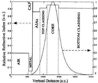
Dependence of refractive index of AC-Gai-n-As on x composition (Fig. 2.10), gives a clue about the choice of a low index material. Pure AlAs having an index of n = 2.9 at our operating wavelength is a step in the right direction.
2.4
Low Loss Waveguide Design
We have studied the effect of converting a 0.4 ¡.mi thickness of 0.8 ¡.irn top A/o.eiFTfio.sgAs layer to AlAs.
1
-D finite difference simulations yield encouraging results (Fig. 2.17).Figure 2.17: Loss Calculation
-1
Loss calculation of waveguide with 0.4 fim AlAs / 0.4 /¿m .
4
/o.(3
iC'ao.,3
g/l.s top claddingThe calculated value of 2.2 dB /cm for TM loss is a large step in eliminating metal loss with respect to the previously calculated loss value of 8.5 dB /cm but this is still unacceptable for operation of most PICs.
Recently, there has been much progress in utilization of oxidized Al„Ga.i_.„As laj^ers in optoelectronic devices. Much of this has been in the area of vertical
cavity surface emitting lasers (VCSELs) where the electrical insulation and low index of the oxidized layers lead to low threshold lasers. This technology has also been used to demonstrate metal-oxide-semiconductor field effect transistor (MOSFET) operation where thin layers of oxidized Ah.Ga.i_^:As layers have been used under the gate.^° The fact that this application shows the possibility of applying electric field to underlying active layers through oxidized AEGai_a:As (AlOx) layers is technologically very important. While passive optical waveguide devices is slowly forthcoming, the real advantage of tlu'se layers in active devices lie in the possibility of applying electric fields through them. The low index combined with this possibility is very promising for a variety of devices including polarization sensitive devices.
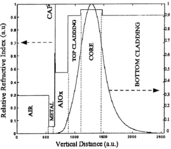
It has been previously reported that the refractive index of AlAs drops drastically from 2.9 to about ~ 1.6 when o x id iz e d .T h e reason for this change in refractive index is the total reconstruction of the chemical composition. Thus AlOx layers provide an even lower index than AlAs layers and hence lead to stronger quenching of the field before it reaches the metal overlaj'^ers. We have included AlOx layers of Vcvrious thickness into our TD finite difference calculations to see the effect on loss. We have found that a thickness of 0.4 /m?. was sufficient and reduced the metal loss down to below
1
dB /cm for TM polarization which is satisfactory (Fig. 2.18).Although the lattice constants of Ah,Gai_i.A.s and y\lyGa.i_,/As crystals for any X and y, are known to be very close, their thermal expansion coefficients were reported to be quite different, giving rise to interface slress on the order of
10
^ dyn/cm^, when grown successively on GaAs substrates.'*·^ In addition, interface stress was known to be an increasing function of the temperature. Thus, our multilayer structure, having a 0.4 /cm x=1.00 layer on top of a y=0.61 layer, was expected to experience high stress, while being oxidized at 100°C. To minimize the possible stress related problems such as surface cracks, we have inserted a100
A
graded x Alj..Gai_3
,-As layer at the Alo.6
iGao.39
A s/A lAs interface. Furthermore, we have changed the top AlAs layer to Alo.98
Gao.02
As to ini])rove lattice matching.CHAPTER 2. THEORY AND DESIGN 30
Figure 2.18: Loss Calculation
-2
Loss calculation of waveguide with 0.4 f.im AlOx / 0.4 ¡.nn .4/o.(3it'V/,o,3<j/Ls top cladding
oxidized version and waveguide structure with a thick Alo.
6
iCao.39
As top cladding layer will be called as W G l, W G2
and WG3 respectivel}·, lor convenience.Changing the index of the material in the rib of the waveguide exposes no risk on single mode operation since the effective index of the waveguide shifted to lower values and normalized parameter V in condition 2.20 tended to take a smaller value. But a slight tuning in the rib height has l)een necessary to enhance the lateral confinement of light.
At the end we have reached our final waveguide designs as in the figures 2.19, 2.20 and 2.21.
: Met^ p J H H H H H B H b ^ · Elocfiode · iL hF=0.6jim Si-2.9 air J w 0.2|^di '-4·"*··’··...w-4.0Uii(i ii=1.0 i J [---^ tt-3.072 i J [ ^ ^ n-3225 i [ dt„»=2.0H.m ii-3.072
J
rSI GaAs Substrate
Figure 2.19: Final Design of W G l Waveguide
’ i J hF=0.6p,m A1 Oxide ii-1.6 1 Metal ^ : Electrode i air n=1.0 ^ 0.2fim ^ W-4.0LUQ ... ... ... . i J [ b t°=02l{xm tt=»3.072 1 j i d.-0.7Hm 1 n-3.225 1 [ di.-2.fl|J.m n-5.072 J r
SI GaAs Substrate
CHAPTER 2. THEORY AND DESIGN 32 : Metal ; h=1.6[xm : Electrode : air J n=1.0 n-3.072 : d,«0.7Um ____ _____ n-3.072
SI GaAs Substrate
Figure 2.21: Final Design of WG3 Waveguide
2.5
Polarization Splitter
The next step of our study was to demonstrate the possible application of loss reducing AlOx layer on an active optoelectronic device performance that required the use of metal electrodes. The polarization s p l i t t e r ^ ^ ^ w a s chosen for this purpose, due to availability of the fabrication masks. The previous studies on this device reported high propagation loss of TM polarized optical excitations due to metal electrodes on a standard multilayer rib waveguide design.
When two identical waveguides are in close proximity of each other, the propagation properties of optical field in the waveguides can not be described separately. When the separation of two waveguides is on the order of waveguide width, the light propagating in any one of them starts to feel the effective index of the other. The structure should be treated as a whole by effective index method and/or BPM. The medium, where the optical field propagates will be composed of two index steps, rather than one. This double waveguide structure will be called a coupler based polarization splitter. The operation principle of the polarization
splitter can be summarized as follows :
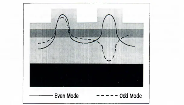
The mode shape of the optical field will be composed of superposition of two eigenmodes. But the complex system should have its own eigenmodes rather than the eigenmodes of the individual Wciveguides.® The light propagation in such a system can be described by the choice of two eigenmodes, one even and one odd with different propagation constants fig and /lo (See Fig. 2.22).
Even Mode
---Odd Mode
Figure 2.22: Electic Field Distribution of the Odd and Even Modes of a Polarization Splitter
The wave equations used to describe this system are called the coupled wave equations. Since the propagation constants of the two modes are different, the field energy will not always be carried in the waveguide, into which it was initially incident. Let us assume that light is initially incident on only one of the waveguides in Fig. 2.22. If we describe the optical field in the coupler’s eigenmode space, the two modes interfere constructively at the input waveguide and destructively in the neighboring waveguide. As the light propagates through the coupler system, the location of constructive inteivference in y direction will shift since a phase delay between even and odd modes will develop in propagation (.?) direction. The optical energy will be totcdly shifted to the neighboring guide
CHAPTER 2. THEORY AND DESIGN 34
when the phase clifFerence becomes ж. Ыепсе we сап say tliat the optical field will be totally moved (coupled) to the other waveguide. The total physical length traversed by the optical field until it is coupled to the other guide will b(' called the coupling lenglli (Lc)· Then, the coupling length can be written as :
Lc = T, ж
A - « .
With the help of effective index method, the parameters fC and thus L^, can be calculated for a given polarization splitter geometry at a given wavelength. The polarization state of optical field will be important in the analysis since two different polarizations will yield different effective indices because of the boundary conditions. Therefore the effective indices, propagafion constants and coupling lengths {hcTE different for TE and I'M polarized fields. This can be regarded as birefringence^ (Fig. 2.23).
WAVEGUIDE COUPLER
POLARIZATION SPLITTER
0
Circularly Polarized Light\
У
... b(,-rM-2L,-cTEr
\
TE Poiarized Light TM Polarized LightAs we intend to investigate the elTects of AlOx layers on polarization splitting, we have simulated the dependence of various geomel rical parameters on coupling length ratios as in Figs. 2.24, 2.25, 2.26, and 2.27.
CHAPTER 2. THEORY AND DESIGN 36
Figure ‘2.25: Coupling Ratio versus Rib Width
Figure 2.27: Coupling Ratio versus An
An is the index difference between core and cladding layers.
These simulations were done by effective index method. We have also done simuhitions by the commercial BPM program.
The figure 2.28 demonstrates midtiple coupling of the TE mode between the two waveguides. Light couples back and forth in the straight section, since the coupling length is smaller than the straight sections of the polarization splitter. The figures 2.29 and 2.30 are for demonstration of polarization splitting. TE polarized light couples twice as TM polarized light couples once, propagating the same length. Hence, when a circularly polarized light is inserted at one of the input ports of the coupler, the TE and TM polarized optical fields exit at different output ports of the device.
CHAPTER 2. THEORY AND DESIGN 38
10
20
30
- 2 0 - 1 0
0
Transverse Direction
Figure 2.28: Multiple Coupling of TE Mode between the two Wa.veguides Light couples back and forth if the straight section length is larger than the coupling length.
" o <D O ~ s o o _
o
L_ CL·8000
7000
6000
5000
4000
3000
2000
1000
0
-2 0 -1 0
0
10 20
30
Transverse Direction (iim)
Figure 2.29: Coupling of TE Polarized Light
The straight section length of the coupler is approximately twice the TE coupling length.
CHAPTER 2. THEORY AND DESIGN 40 " o <D O
o
o o C l O !> _ Q_8000
7000
6000
5000
4000
3000
2000
1000
0
-2 0 -1 0
0
10
20
30
Transverse Direction (tim)
Figure 2.30: Coupling of TM Polarized Light
The straight section length of the coupler is approximately equal to the TM coupling length.