1 Department of Physics, Bilkent University, Ankara 06800, Turkey. 2 Department of Electrical and Electronics Engineering, Bilkent University, Ankara 06800, Turkey. 3 The Center for Solar Energy Research and Applications, Middle East Technical University, Ankara 06800, Turkey. 4 Department of Electrical Engineering and Computer Science, Massachusetts Institute of Technology, Cambridge, MA 02139, USA. 5 Helmholtz-Zentrum Dresden-Rossendorf, Institute of Ion Beam Physics and Materials Research, Bautzner Landstraße 400, 01328 Dresden, Germany. 6 Micro and Nanotechnology Graduate Program, Middle East Technical University, Ankara 06800, Turkey. 7 Department of Physics, Middle East Technical University, Ankara 06800, Turkey. 8 Harvard Medical School, Boston, MA 02115, USA. 9 Izmir International Biomedicine and Genome Institute, Izmir 35340, Turkey. 10 UNAM – National Nanotechnology Research Center and Institute of Materials Science and Nanotechnology, Bilkent University, Ankara 06800, Turkey. Onur Tokel and Ahmet Turnalı contributed equally to this work. *e-mail: [email protected]
Silicon is an excellent material for microelectronics and inte-grated photonics1–3, with untapped potential for mid-infrared optics4. Despite broad recognition of the importance of the third dimension5,6, current lithography methods do not allow the fabrication of photonic devices and functional microel-ements directly inside silicon chips. Even relatively simple curved geometries cannot be realized with techniques like reactive ion etching. Embedded optical elements7, electronic devices and better electronic–photonic integration are lack-ing8. Here, we demonstrate laser-based fabrication of com-plex 3D structures deep inside silicon using 1-µ m-sized dots
and rod-like structures of adjustable length as basic building blocks. The laser-modified Si has an optical index different to that in unmodified parts, enabling the creation of numer-ous photonic devices. Optionally, these parts can be chemi-cally etched to produce desired 3D shapes. We exemplify a plethora of subsurface—that is, ‘in-chip’—microstruc-tures for microfluidic cooling of chips, vias, micro-electro-mechanical systems, photovoltaic applications and photonic devices that match or surpass corresponding state-of-the-art device performances.
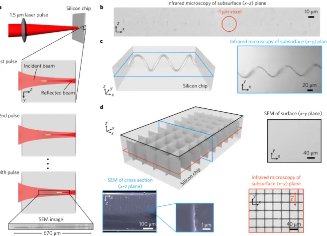
Efforts to modify silicon below the surface using a pulsed laser go back more than a decade9, albeit with limited success (for a review see Supplementary Section 1). We begin by discussing point-like modification of Si at the laser focus, based on an approach we have demonstrated previously10. We use a custom-developed nanosec-ond-pulsed fibre laser11 operating at a central wavelength of 1.55 µ m, where Si is transparent. Using a × 40 objective to focus the beam tightly, we trigger a set of light–matter interaction mechanisms simultaneously (Supplementary Section 2), leading to well-con-trolled and repeatable beam collapse (Fig. 1a). When only a single pulse is applied, this results in permanent modification of the crystal structure (Supplementary Section 3) within a roughly 1-µ m-wide spherical region (Fig. 1b). By repositioning the beam and sending a single pulse to each new position, any desired 3D structure, like the 1-µ m-thick, 1-mm-long helix in Fig. 1c, can be created, point by
point. However, like all 3D fabrication methods, there is an inherent trade-off between resolution, speed and processing volume12. We provide numerous examples of structures and devices in Figs. 3 and 4, which occupy volumes ranging between 0.1 and 10 mm3.
Point-by-point processing of such macroscopic volumes with 1 µ m resolu-tion requires approximately 108–1010 beam-positioning steps, which
leads to prohibitively long processing times, limited by the speed of modern beam-positioning equipment. We circumvent this problem by augmenting point-by-point processing with the creation of self-organized rod-like structures forming along the beam propagation direction. This works well in practice, because most 3D structures of interest can be broken down into rods of various lengths (rods grow in length with the number of incident pulses). If the structure requires finer features, these can be created by additional point-by-point processing. In this way, the fabrication time is reduced from thousands of hours to mere minutes.
To trigger the self-organized pulse-to-pulse growth of the rod-like structures, we invoke nonlinear feedback mechanisms13–16 arising from the interaction of infrared laser pulses inside Si: (1) competing thermal nonlinearity- and free-carrier-induced (FCI) refractive index changes due to counter-propagating laser beams, and (2) a self-limiting, non-local feedback loop arising from per-manent local modification of Si at the beam focus, which, in turn, iteratively shifts the focal position of the beam, resulting in rod-like structures whose lengths are controlled by the number of incident pulses. The beam, focused by a lens, passes through the Si chip. About a third of it returns from the back surface of the chip due to Fresnel reflection, and counter-propagates with respect to the inci-dent beam (Fig. 1a). Near its focal point, positioned at a desired point inside the chip, the beam collapses due to nonlinear effects and modifies the Si. When additional pulses are sent, their focal points iteratively shift along the optical (z) axis as each pulse further modifies the material, changing the optical path of the next pulse (Fig. 1a). The beam width is unaltered, so the structured region progressively gets longer without increasing in width, and its aspect ratio can reach far beyond the diffraction limit. By repositioning the
In-chip microstructures and photonic devices
fabricated by nonlinear laser lithography deep
inside silicon
Onur Tokel
1*, Ahmet Turnalı
2, Ghaith Makey
1, Parviz Elahi
1, Tahir Çolakoğlu
3, Emre Ergeçen
4,
Özgün Yavuz
2, René Hübner
5, Mona Zolfaghari Borra
3,6, Ihor Pavlov
1, Alpan Bek
3,6,7, Raşit Turan
3,6,7,
Denizhan Koray Kesim
2, Serhat Tozburun
8,9, Serim Ilday
1and F. Ömer Ilday
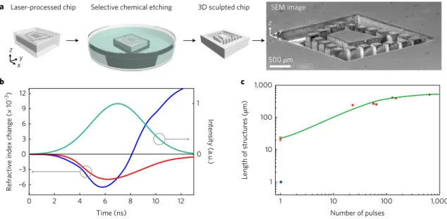
1,2,10beam and sending a controlled number of pulses, we create elon-gated structures of controllable length (Fig. 2c) at desired locations within the chip, which are combined to construct complex struc-tures (Fig. 1c,d). After this single-step procedure, the Si chip has only internal refractive index modification, which is used to dem-onstrate a variety of optical elements, such as lenses, holograms and waveguides. As an optional second step, we can selectively remove the modified regions by chemical etching to enable full 3D sculpting of the entire chip. For instance, the fabrication of ‘Penrose stairs’17 is illustrated in Fig. 2a.
We explain the self-organization physics governing the cre-ation of the structures by using a toy model (see Supplementary Section 4 for details) to qualitatively illustrate the basic forma-tion mechanism. Wave propagaforma-tion is governed by the nonlinear paraxial equation and the heat equation. This equation system is mathematically equivalent to the Newton–Schrödinger system18. Two competing diffractive effects dominate beam propagation, a thermally induced change of the index of refraction (Δ ntherm) and a
free-carrier-induced (FCI) refractive index change (Δ nFCI), which
are similar to concatenated converging and diverging lenses with focal lengths ftherm and fFCI, respectively. Modification of Si occurs
if the beam self-focuses and collapses (the first feedback mecha-nism), which requires the thermal lensing to be stronger than diffraction due to the FCI effect (ftherm < |fFCI|). The incident and
reflected beams are individually too weak to modify the material
(ftherm > |fFCI|), but when overlapped, they cooperate to modify the
crystal structure permanently (Fig. 2b). This scenario was verified by numerical solutions of beam propagation based on the split-step Fourier method (Supplementary Section 2), which show that shielding due to negative Δ nFCI precludes subsurface
modifi-cation for a single beam, consistent with experiments. In contrast, thermal lensing is enhanced when the beams are coupled (Figs. 1a and 2b) and the beam collapses to induce permanent refractive index changes in the Si. When more than one pulse is incident, the second feedback mechanism is activated. Each pulse locally modi-fies the Si, and the resulting change in refractive index shifts the focal point for the next pulse, in a manner similar to the moving focus model of self-focusing19. The focal position of the second pulse, l2, is given by
= + +
l12 fFCI1 ftherm1 l11
where l1 is the focal position of the first pulse. The location of the
modification caused by the nth pulse (n > 1), ln, is found from
= − + + l1 ( 1) 1n f f l 1 1 n FCI therm 1 z y x Silicon chip SEM image 1st pulse 2nd pulse Nth pulse 670 µm Silicon chip 1.5 µm laser pulse Incident beam Reflected beam d b a 40 µm Infrared microscopy of subsurface (x–y) plane
ε x y x z 100 µm
SEM of cross section (x–z plane)
1 µm
40 µm SEM of surface (x–y plane)
x y z y x y c Silicon chip z y x
Infrared microscopy of subsurface (x–y) plane
20 µm 10 µm ~1 µm voxel
x z
Infrared microscopy of subsurface (x–z) plane
Fig. 1 | creation of 3D index modification inside Si. a, Schematic showing laser pulses incident on a Si chip. The pulse collapses and modifies the local Si
crystal structure, which constitutes a building block for more complex structures. Consecutive laser pulses focus to shifted positions, axially elongating the structured region. Inset: scanning electron microscopy (SEM) image of a rod-like structure in Si. b, Infrared image of an array of 1-µ m-sized voxels, each created by a single laser pulse. c, Infrared image of a 1-µ m-thick, 1-mm-long helix, exemplifying point-by-point fabrication of an in-chip 3D structure.
d, Various 3D structures can be formed using rod-like structures as building blocks. These 1-µ m-wide structures can range from 20 µ m to hundreds of micrometres in length along the laser propagation direction (z axis). SEM (top surface and cross-section) and infrared transmission microscope (subsurface) images correspond to colour-labelled planar sections in the 3D schematic. The subsurface mesh is directly revealed in the infrared image, whereas the top (shown) and bottom (not shown) surfaces remain unscathed. In all figures, the z axis is the optical axis.
The total length is then ξ = − = + ∕ − l l l l n 1 ( 1) n total 1 1 where ξ = +
(
f f)
l f f FCI therm 1 FCI thermis a constant. This result reveals that elongation of the structures is self-limiting, stopping before reaching the chip surface (Fig. 2c).
We now discuss the features and limitations of creating general 3D structures out of the rod-like building blocks. First, we verify that continuous, wall-like structures can be created by translating the beam in a plane perpendicular to the beam propagation direc-tion (z axis) (Fig. 1d and Supplementary Video 1). Cross-sectional microscope images show that the lengths of the structures range from the Rayleigh length (~20 µ m, Fig. 2c) to ~1 mm (limited by the thickness of the chip), while always retaining a width of ~1 µ m (Fig. 1d). The corresponding aspect ratio approaches 1,000, which is only possible due to the iterative formation mechanism, where pre-viously formed structures are likely to be seeding the process of their elongation. Next, we verify that the structures can cross over each other without distortion, as evidenced by the mesh structure shown in Fig. 1d. We also confirm that curvilinear structures can be formed (note the spiral in Supplementary Fig. 14). None of these features were obvious, a priori, due to the self-organized nature of the for-mation mechanism. There is no fundamental limit to the area over which the structures can be created. Similarly, doping of Si is not a limitation; we can create structures in both intrinsic and doped Si. A complete set of experiments is provided in Supplementary Section 5 for n- and p-doped Si chips, where the effects of polarization,
scanning angle and direction are analysed. Furthermore, we do not observe any asymmetry resulting from the scanning direction or polarization of the beam, which is not surprising given that Si is a centrosymmetric material20.
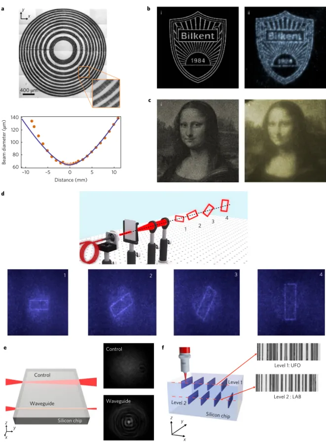
We first discuss demonstrations based on purely internal index modification of the Si chip, followed by those where the chip is selectively etched to reveal a desired 3D architecture. There is much interest in using Si as a material for mid-infrared applica-tions4. The capability to locally modify the index of refraction in a well-controlled manner affords unprecedented spatial phase con-trol over optical beams. As an example, we demonstrate the first in-chip Fresnel zone plate (FZP) lens (Fig. 3a). The focal length f is determined by Rk= kfλ+(kλ∕2)2, where Rk is the radius of
the kth zone and λ is the wavelength. An FZP is designed with R20= 1.5 mm, f = 7.2 cm at 1.55 µ m. The performance is evaluated to
give f = 7.3 cm, M2= 1.46 (Fig. 3a) with 15% diffraction efficiency,
which exceeds that of single-layer FZP lenses created in glass. Additional applications of creating a refractive index distri-bution inside Si include wavefront structuring21–23, flat optics24, adaptive optics25, Si photonics1 and better electronic–photonic integration26. We showcase this capability through the creation of 2D Fourier computer-generated holograms (CGHs) for binary (Fig. 3b) and greyscale (Fig. 3c) images and Fresnel (Fig. 3d) CGHs for 3D images, all designed using a customized adaptive-additive iterative Fourier transform algorithm (Supplementary Section 6). The experimentally reconstructed binary hologram, composed of 600 × 600, 10 µ m pixels, is shown in Fig. 3b. Reproduction of high-frequency spatial components in holography is notoriously difficult26. The fact that they are reproduced in Si with high qual-ity is a confirmation of the good control we have over index modi-fications (Fig. 3b). Greyscale images require even more advanced wavefront structuring, which we demonstrate through a 600 × 600, 10 µ m pixel hologram (Fig. 3c). The pixel count and image recon-struction quality of our in-chip holograms are comparable to those of state-of-the-art nanophotonic phase arrays22 and metamaterial
b –6 –3 0 3 6 9 12
Refractive index change
(× 10 –3) 1 0 Intensity (a.u.) SEM image z y x Laser-processed chip Selective chemical etching 3D sculpted chip
500 μm z y x a c
Time (ns) Number of pulses
Length of structures (μ m) 1,000 100 10 1 0 2 4 6 8 10 12 1 10 100 1,000
Fig. 2 | Selective chemical etching and theoretical modelling. a, Illustration summarizing single-step selective chemical etching for removal of the
laser-processed volumes. The SEM image shows the experimental realization of ‘Penrose stairs’17. b, Simulation results show a self-induced refractive index
change, composed of thermal nonlinearity- (positive Δ nthermal) and free-carrier-induced refractive index change (negative Δ nFCI) for a single pulse (green curve). The red curve shows the self-induced refractive index change for a single beam focused in Si. The blue curve shows the index change for the two counter-propagating beams. Thermal nonlinearity is dominant in the latter, enabling beam collapse and modification in Si. c, Comparison of the
prediction of our analytical model for structure elongation with each pulse, with experimental results. Data points represented by red circles were created using a lens with numerical aperture (NA) of 0.55 and the isolated data point (blue diamond) was created using an objective with NA of 0.75. In all figures, the z axis is the optical axis.
Waveguide Control 1 2 3 4 1 2 3 4 Silicon chip Level 1 Level 2 z y x Level 1: UFO Level 2 : LAB b c d e i ii i ii 400 μm x y a f Control Waveguide z y x Silicon chip Beam diameter (µ m) Distance (mm) 140 120 100 80 60 –10 –5 0 5 10
Fig. 3 | Functional in-chip optical elements and information storage. a, Top: composite infrared transmission microscope image of a subsurface FZP lens.
Inset: close-up view. Bottom: theoretical and experimental beam profiles during focusing. b, Simulation of a binary image with high-frequency spatial
components, from a hologram of 600 × 600 pixels (i), and experimental reconstruction of the hologram written in Si (ii). c, Simulation of a grey-scale image of Mona Lisa, from a hologram of 600 × 600 pixels (i), and experimental reconstruction of the hologram written in Si (ii). d, 3D holography of a rotating rectangle at four consecutive planes (top). The Fresnel-type hologram in Si is composed of 800 × 600 pixels. Experimentally reconstructed images of the projected rectangles are shown below. All holograms have 10-µ m-sized square pixels. e, Measured far-field intensity profiles corresponding to the beam traversing a region without a waveguide (control) and a laser-written waveguide. f, Illustration of multilevel information storage and measured
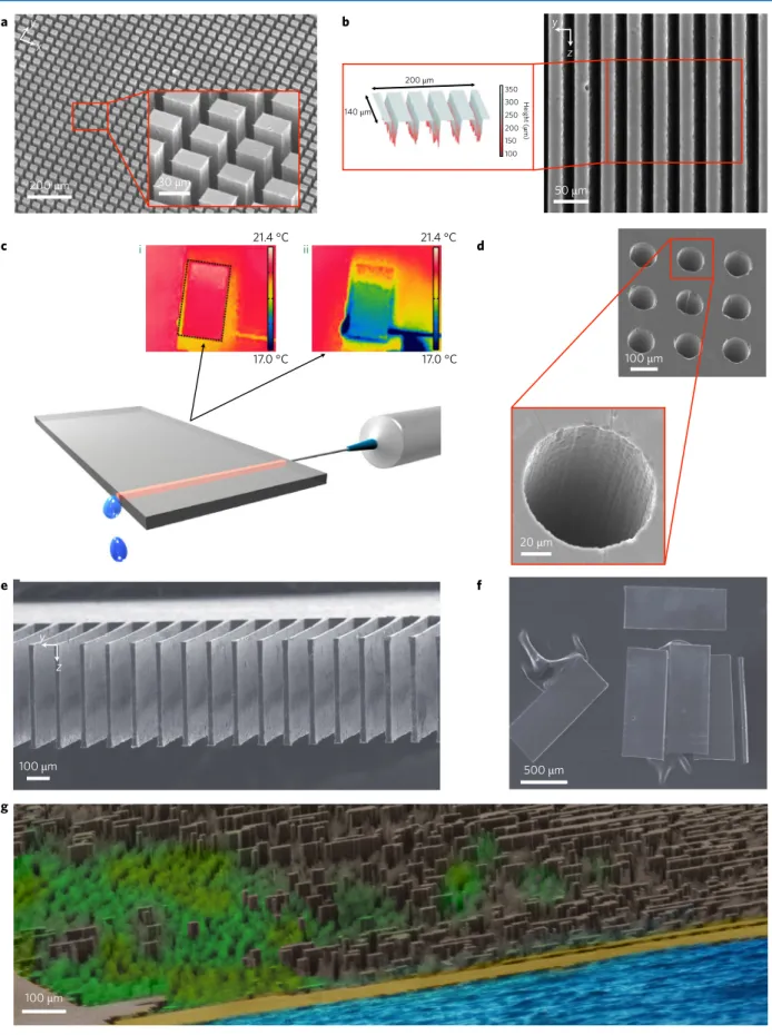
a b d e g f c 100 μm 100 μm 20 μm 50 μm 100 μm 30 μm 200 μm y z y x y z 500 μm i ii 200 μm 140 μm 350 300 250 200 150 Height (μ m) 100 21.4 °C 17.0 °C 17.0 °C 21.4 °C
Fig. 4 | Sculpting of 3D arbitrary micro-architectures. a, SEM image of large-area-covering, high-aspect-ratio micropillars revealed after chemical etching.
Inset: close-up view of the etched micropillar array. The pillars have 20 × 30 µ m top surfaces and their heights extend ~500 µ m along the laser propagation direction. b, SEM image of a sidewall of a Si chip, showing embedded microchannels. Inset: laser scanning microscopy of the channels, which penetrate
hundreds of micrometres into the chip. c, Illustration of an 8-mm-long microfluidic channel carrying cooling water into a chip. Thermal camera images
before (i) and after (ii) passing the water show that the surface temperature of the chip decreases by 4 °C within a few seconds. d, SEM images of the
entrances of through-Si vias that cut across the entire chip. e, SEM image of 3D cantilever-like structures. f, SEM image of controlled slicing of a chip into
phase holograms23,26. We also note that Si is CMOS-compatible and lossless over a broad spectral range, including telecommuni-cation wavelengths and much of the mid-infrared27. Finally, we demonstrate holography of a 3D image using a Fresnel hologram (800 × 600, 10 µ m pixels), which projects rotating rectangles at consecutive planes (Fig. 3d and Supplementary Video 2). This is achieved by first combining a stack of Fourier holograms, each gen-erating a 2D slice of an intended 3D object and then superimposing them with FZPs, which shift each image to its corresponding focal plane (Supplementary Section 6). This construction itself is novel, where the phase-type Fresnel hologram can be generated without directly using the Fresnel equation. To assess the hologram effi-ciency28 R, gratings were written in Si, with
ϕ ϕ = Δ π − + Δ R F F F 4 sin ( ) (1 cos ( )) 2 2 2
where Δ φ is the phase modulation and F is the filling factor. The measured first-to-zero-order ratio, R ~ 150%, corresponds to Δ φ = 0.69π ± 0.04π , which compares well with the directly mea-sured Δ φ = 0.69π ± 0.01π .
As final applications of the purely optical modification of Si, we demonstrate the formation of an optical waveguide (Fig. 3e) and in-chip information storage (Fig. 3f). For the former, we created a 2.5-mm-long tubular waveguide structure (the laser-processed regions have a depressed index of refraction). The radius of the core region is 10 µ m. The far-field intensity profile of the beam obtained at the exit of the Si chip is shown in Fig. 3e, where an identical mea-surement of the beam traversing a region without a waveguide is also provided as control. For the latter, we created multi-level (more than 500 levels are theoretically possible assuming a 1-mm-thick chip, but, as proof of principle, 25 were written, 7 of which can be directly seen in Supplementary Video 3) buried structures arranged in a dot or barcode format. Next, we created a two-level barcode, where the levels spell ‘UFO’ and ‘LAB’ (Fig. 3f). We limited ourselves to two levels for ease of readout, which was achieved by optical coherence tomography. Furthermore, laser-written structures could be erased following exposure to high temperatures (1,100 °C) in an oven for 2 h. Afterwards, the same digital readout protocol that correctly detected 96% of the written dots false-detected only 3% of erased dots (Supplementary Section 5), highlighting the prospects for eras-able and rewriteras-able information storage and holography. This pro-cess could probably be simplified and rendered spatially selective by using continuous-wave laser heating instead of an oven.
The second class of applications is based on selective chemi-cal etching of the optichemi-cally processed chip for truly 3D sculpting (Fig. 4). Thanks to the vastly higher etching rates for modified parts of Si compared to unmodified parts, we are able to create extremely regular arrays of sharp-edged and high-aspect-ratio (20 µ m × 30 µ m × 500 µ m) pillars within minutes (Fig. 4a and Supplementary Section 7). Among the numerous possible applications, there is the possibility to create buried microfluidic channels (Fig. 4b). Pumping coolants directly through microfluidic channels written inside chips is being considered as a possible remedy to the overheating of microprocessor chips29, which is a main limitation to increasing clock rates30. As a proof-of-principle experiment, we passed cold water through a Si chip, which decreased the surface temperature by 4 °C within a few seconds (Fig. 4c and Supplementary Video 4). As another potential application of 3D sculpting to electronics, we demonstrate through-Si vias31 of controllable depth, including those that cut across the entire chip (Fig. 4d). Furthermore, in Fig. 4e we present 3D cantilever-like structures that could find use in micro-electro-mechanical systems (MEMS) applications. We also show controlled slicing of a chip into ~30-µ m-thick plates (Fig. 4f). To this end, planar sections inside the chip are raster-scanned with
laser pulses, followed by chemical etching, resulting in mechanical separation of the chip along the processed planes. The sliced plates can be used for photovoltaic cell fabrication, for example, reduc-ing the required amount of Si material by an order of magnitude, with potential for major cost reductions. As a final illustration of the potential for 3D sculpturing, we created a microscale Si city, Siliconopolis, with representations of buildings, trees, a beach and a sea (Fig. 4g).
We have outlined a general methodology and the various exam-ples demonstrated here are far from constituting an exhaustive list. Additional possibilities include the creation of in-chip microlens arrays, microresonators, modulators for multi-level electronic–pho-tonic integration and rewritable holograms or information storage.
Methods
Methods, including statements of data availability and any associ-ated accession codes and references, are available in the online ver-sion of this paper.
Received: 26 January 2017; Accepted: 25 July 2017; Published online: 29 September 2017
References
1. Leuthold, J., Koos, C. & Freude, W. Nonlinear silicon photonics. Nat. Photon. 4, 535–544 (2010).
2. Priolo, F., Gregorkiewicz, T., Galli, M. & Krauss, T. F. Silicon nanostructures for photonics and photovoltaics. Nat. Nanotech. 9, 19–32 (2014).
3. Lim, A. E.-J. et al. Review of silicon photonics foundry efforts. IEEE J. Sel. Top. Quantum Electron. 20, 405–416 (2014).
4. Soref, R. Mid-infrared photonics in silicon and germanium. Nat. Photon. 4, 495–497 (2010).
5. Emma, P. G. & Kursun, E. Is 3D chip technology the next growth engine for performance improvement? IBM J. Res. Dev. 52, 541–552 (2008).
6. Wong, H.-S. P. & Salahuddin, S. Memory leads the way to better computing. Nat. Nanotech. 10, 191–194 (2015).
7. Beresna, M., Gecevičius, M. & Kazansky, P. G. Ultrafast laser direct writing and nanostructuring in transparent materials. Adv. Opt. Photon. 6, 293–339 (2014).
8. Sherwood-Droz, N. & Lipson, M. Scalable 3D dense integration of photonics on bulk silicon. Opt. Express. 19, 17758–17765 (2011).
9. Nejadmalayeri, A. H., Herman, P. R., Burghoff, J., Will, M., Nolte, S. & Tünnermann, A. Inscription of optical waveguides in crystalline silicon by mid-infrared femtosecond laser pulses. Opt. Lett. 30, 964–966 (2005). 10. Pavlov, I., Dülgergil, E., Ilbey, E. & Ilday, F. Ö. Conference on Lasers and
Electro-Optics 2012, CTu2M.5 (Optical Society, San Jose, CA, USA, 2012). 11. Pavlov, I., Dülgergil, E., Ilbey, E. & Ilday, F. Ö. Diffraction-limited, 10-W, 5-ns, 100-kHz, all-fiber laser at 1.55 μ m. Opt. Lett. 39, 2695–2698 (2014). 12. Truby, R. L. & Lewis, J. A. Printing soft matter in three dimensions. Nature
540, 371–378 (2016).
13. Öktem, B. et al. Nonlinear laser lithography for indefinitely large-area nanostructuring with femtosecond pulses. Nat. Photon. 7, 897–901 (2013). 14. Arecchi, F. T., Boccaletti, S. & Ramazza, P. L. Pattern formation and
competition in nonlinear optics. Phys. Rep. 318, 1–83 (1999).
15. Kerse, C. et al. Ablation-cooled material removal with ultrafast bursts of pulses. Nature 537, 84–88 (2016).
16. Ilday, S. et al. Multiscale self-assembly of silicon quantum dots into an anisotropic three-dimensional random network. Nano Lett. 16, 1942–1948 (2016).
17. Penrose, L. S. & Penrose, R. Impossible objects: a special type of visual illusion. Br. J. Psychol. 49, 31–33 (1958).
18. Bekenstein, R., Schley, R., Mutzafi, M., Rotschild, C. & Segev, M. Optical simulations of gravitational effects in the Newton–Schrodinger system. Nat. Phys. 11, 872–878 (2015).
19. Brodeur, A. et al. Moving focus in the propagation of ultrashort laser pulses in air. Opt. Lett. 22, 304–306 (1997).
20. Yang, W., Kazansky, P. G. & Svirko, Y. P. Non-reciprocal ultrafast laser writing. Nat. Photon. 2, 99–104 (2008).
21. Kildishev, A. V., Boltasseva, A. & Shalaev, V. M. Planar photonics with metasurfaces. Science 339, 1232009 (2013).
22. Sun, J., Timurdogan, E., Yaacobi, A., Hosseini, E. S. & Watts, M. R. Large-scale nanophotonic phased array. Nature 493, 195–199 (2013). 23. Zheng, G. et al. Metasurface holograms reaching 80% efficiency.
Nat. Nanotech. 10, 308–312 (2015).
24. Yu, N. & Capasso, F. Flat optics with designer metasurfaces. Nat. Mater. 13, 139–150 (2014).
25. Wang, Q. et al. Optically reconfigurable metasurfaces and photonic devices based on phase change materials. Nat. Photon. 10, 60–65 (2016).
26. Larouche, S., Tsai, Y.-J., Tyler, T., Jokerst, N. M. & Smith, D. R. Infrared metamaterial phase holograms. Nat. Mater. 11, 450–454 (2012).
27. Wu, C. et al. Spectrally selective chiral silicon metasurfaces based on infrared Fano resonances. Nat. Commun. 5, 3892 (2014).
28. Li, X. et al. Athermally photoreduced graphene oxides for three-dimensional holographic images. Nat. Commun. 6, 6984 (2015).
29. Dang, B., Bakir, M. S., Sekar, D. C., King, C. R. Jr & Meindl, J. D. Integrated microfluidic cooling and interconnects for 2D and 3D chips. IEEE Trans. Adv. Pack. 33, 79–87 (2010).
30. Ball, P. Feeling the heat. Nature 492, 174–176 (2012).
31. Motoyoshi, M. Through-silicon via (TSV). Proc. IEEE 97, 43–48 (2009).
Acknowledgements
This work was supported partially by a European Research Council (ERC) Consolidator Grant ERC-617521 NLL, EU Marie Curie Fellowship 660769 SMILE and TÜBITAK under project 113M930. The authors acknowledge support from the Structural Characterization Facilities at IBC of the HZDR. The authors thank H. Volkan Hünerli for discussions of the chemical procedure.
Author contributions
O.T. and F.Ö.I designed the research and interpreted the results, with help from S.I. Experiments were performed by A.T., O.T., G.M. and Ö.Y. The customized laser was built by I.P. The analytical model was developed by P.E., O.T. and F.Ö.I. Numerical simulations were performed by A.T., O.T. and E.E. Chemical etching was developed by T.Ç., M.Z.B., A.B. and R.T. Material analyses were performed by R.H. and S.I. Waveguide characterization and optical coherence tomography imaging were performed by D.K.K. and S.T., respectively.
competing interests
The authors declare no competing financial interests.
Additional information
Supplementary information is available for this paper at doi:10.1038/s41566-017-0004-4.
Reprints and permissions information is available at www.nature.com/reprints.
Correspondence and requests for materials should be addressed to T.O.
Publisher’s note: Springer Nature remains neutral with regard to jurisdictional claims in
Methods
Experimental set-up. We used optical pulses with a central wavelength of 1.55 µ m, duration of 5 ns and repetition rate of 150 kHz (Supplementary Section 8). The laser system was coupled to a processing station with precise alignment, power and polarization control. For single-point modification, a × 40 objective with NA of 0.75 was used. For rod-like structures, the laser was focused to ~3 µ m (f = 4.5 mm, NA = 0.55) after the back surface of a Si sample, which produced the counter-propagating beam. The samples were translated with a three-axis high-resolution computer-controlled stage (Aerotech, ANT130-XY, ANT95-L-Z). The pulse energy was controlled by a half-wave plate between two polarising beamsplitters (PBSs) operating as an attenuator, while the polarization was linear after the PBS and in the plane of the sample surface. A second half-wave plate was used to control the polarization angle. Pulse energies were in the range of 2–8 µ J and 15–20 µ J for single-point and rod-like structures, respectively. The modification threshold was estimated to be 5–15 GW cm–2. Experiments were performed at room temperature and in an ambient atmosphere. We anticipate that the multi-beam-, multi-pulse-based rod-like structures can also be realized in other geometries, such as crossed-laser beams. We used the current architecture for its practical value and simplicity. Optical coherence tomography and infrared microscopy. To validate the 3D information encoding/decoding capabilities in Si, we used a second-generation optical coherence tomography system called optical frequency-domain imaging (OFDI). The OFDI system uses a polygon filter-based wavelength-swept laser source operating at an axial scan rate of 50 kHz. The sweeping range was over 120 nm at a centre wavelength of 1.3 µ m, providing 6 µ m axial resolution in air (~1.8 µ m in Si). The optical interference signals were digitalized and directly transferred to a hard-drive storage array by a two-channel 100 MS s–1 data acquisition board (Signatec). Approximately 10% of the acquired data were employed and processed on the CPU for real-time structural image feedback. We used a homemade scanner microscope comprising a two-axis galvanometer mirror system (GVS112, Thorlabs) and a × 10 scan lens (LSM02, Thorlabs) for barcode decoding. The barcodes use international symbology UPC, code 128.
A homemade infrared microscope was used to evaluate the subsurface structures. This incorporated a broad-spectrum halogen lamp as the light source and an electron-multiplying charge-coupled device camera (Andor, Luca S) as the detector. The infrared microscope was operated in transmission mode with a × 20 objective (Nikon, 0.45 NA × 20). Laser-written samples were studied with a reflection-mode optical microscope (Nikon, 0.6 NA, × 40) and also with scanning electron microscopy (SEM) imaging, confirming that there were no photo-induced
modifications on either side of the wafer. In addition, the etching results provided additional confirmation of undamaged surfaces after laser writing.
Sample preparation, positioning and scanning. Double-side-polished, 〈 100〉 -cut, p-type Si samples (boron-doped, 1 Ω cm and 15 kΩ cm) and n-type (phosphorus-doped, 1 Ω cm) samples were used (Siegert Wafer). Wafers (500 µ m–1.3 mm thick) were diced into 15 mm × 30 mm dimensions. Piranha solution was applied to the samples (2 min), then they were cleaned in acetone (5 min), ethanol (5 min) and deionized water (5 min) and finally dried with nitrogen. The Si samples were held in position with neodymium magnets. Precise sample alignment with respect to the laser was found to be crucial. This alignment was accomplished by using the interference of multiple reflections from the sample’s polished surfaces, which was monitored with an infrared-sensitive camera. The scheme allowed alignment within a few micrometres throughout the scanning range and also operated as a proxy for in situ imaging. The scans were performed in a plane perpendicular to the laser propagation direction at speeds in the 0.2–7 mm s–1 range.
Chemical etching procedure. Chemical etching was applied to optically processed Si samples after the following preparation steps. The samples were first lapped down 150–250 µ m from the surface (Allied High MultiPrep). Consecutive lapping steps were applied with progressively smaller diamond-particle decorated films (with sizes of 35 µ m, 9 µ m, 6 µ m and 0.5 µ m). Further polishing was then performed using an alumina suspension (particle size of 50 nm) until a mirror-like surface was obtained. To prevent contamination, the polished surface was cleaned with the Radio Corporation of America (RCA) clean procedure (RCA-1 and RCA-2 steps). The samples were then exposed to the etching solution for a few minutes, with molar concentrations of the components, Cu(NO3)2, HF, HNO3 and CH3COOH, of 0.05 M, 10 M, 4 M and 3.5 M, respectively (Supplementary Section 7). Finally, the samples were rinsed with deionized water and dried with nitrogen flow. All chemicals were supplied by Merck Chemical Company. The average surface roughness of the top surfaces of the etched structures was measured to be ~20 nm using atomic force microscopy. Although the side surfaces could not be measured directly, we estimated the roughness to be better than ~1 µ m. These values are comparable to or smaller than our smallest feature size of 1 µ m and the infrared wavelengths for which Si is highly transparent (from ~1 µ m to ~9 µ m). Data availability. The data that support the plots within this paper and other findings of this study are available from the corresponding author upon reasonable request.