High-E
fficiency Light-Emitting Diodes of
Organometal Halide Perovskite Amorphous
Nanoparticles
Jun Xing,
†Fei Yan,
‡Yawen Zhao,
§Shi Chen,
†Huakang Yu,
†Qing Zhang,
†Rongguang Zeng,
§Hilmi Volkan Demir,
†,‡,∥Xiaowei Sun,
‡Alfred Huan,
†and Qihua Xiong
*
,†,⊥†Division of Physics and Applied Physics, School of Physical and Mathematical Sciences, Nanyang Technological University,
Singapore 637371
‡LUMINOUS! Center of Excellence for Semiconductor Lighting and Displays, TPI-The Photonics Institute, School of Electrical and
Electronic Engineering, Nanyang Technological University, Singapore 639798
§China Academy of Engineering Physics, Mianyang 621900, China
∥Department of Electrical and Electronics Engineering, Department of Physics, UNAM−Institute of Materials Science and
Nanotechnology, Bilkent University, Ankara 06800, Turkey
⊥NOVITAS, Nanoelectronics Centre of Excellence, School of Electrical and Electronic Engineering, Nanyang Technological
University, Singapore 639798
*
S Supporting InformationABSTRACT: Organometal halide perovskite has recently emerged as a very promising family of materials with augmented performance in electronic and optoelectronic applications including photovoltaic devices, photodetectors, and light-emitting diodes. Herein, we propose and demonstrate facile solution synthesis of a series of colloidal organometal halide perovskite CH3NH3PbX3 (X = halides) nanoparticles with amorphous structure, which exhibit high quantum yield and tunable emission from ultraviolet to near-infrared. The growth mechanism and photoluminescence properties of the perovskite amorphous nanoparticles were studied in detail. A high-efficiency green-light-emitting diode based on amorphous CH3NH3PbBr3
nano-particles was demonstrated. The perovskite amorphous nanoparticle-based light-emitting diode shows a maximum luminous efficiency of 11.49 cd/A, a power efficiency of 7.84 lm/W, and an external quantum efficiency of 3.8%, which is 3.5 times higher than that of the best colloidal perovskite quantum-dot-based light-emitting diodes previously reported. Ourfindings indicate the great potential of colloidal perovskite amorphous nanoparticles in light-emitting devices.
KEYWORDS: organometal halide perovskite, nanoparticles, light-emitting diodes, electroluminescence, photoluminescence
T
he recent progress on organometal halide perovskites as solar cell material has witnessed a remarkable breakthrough in power conversion efficiency over 20%.1,2 Shockley and Queisser showed that high solar cell efficiency is concurrently accompanied by a high concentration of carriers and strong emission of photons.3,4 More recently, organometal halide perovskites have been shown to possess high photoluminescence quantum efficiency (PLQE),5−8 superior electric properties, and unique band structures that make perovskite materials suitable for high-performance, low-cost, large-area, and lightweight light-emitting diodes (LED).9−24However, the organometal halide perovskite LED (PeLED) device performance is still constrained by the delocalization nature and weak exciton binding energy of theperovskite thinfilm, leading to spontaneous dissociation of the exciton into free carriers in the bulk recombination layer, as well as low PLQE, high leakage current, and low luminous efficiency. Therefore, to obtain a high luminous efficiency, the electron and hole must be confined to facilitate their radiative recombination, such as the inorganic LED with a quantum well structure, inorganic quantum dot LEDs based on the quantum confinement effect, and organic LEDs using an amorphous emitting layer.25−32 Received: March 2, 2016 Accepted: June 10, 2016 Published: June 10, 2016
Article
www.acsnano.orgDownloaded via BILKENT UNIV on December 23, 2018 at 18:24:41 (UTC).
Recently, the green perovskite LED was reported to reach a high external quantum efficiency (EQE) of 8.53% by decreasing the particle size of the perovskite-emitting layer as well as increasing the PLQE to 36%,33which reduces the technical gap between PeLED and OLED or inorganic quantum dot LEDs. Moreover, the colloidal perovskite nanoparticles (NPs) with sizes less than 10 nm proved to feature a high PLQE (>90%), and a large exciton binding energy probably opens a way to further improve the performance of PeLED.6,7Herein, we have successfully synthesized the colloidal perovskite CH3NH3PbX3 (X = halides) NPs with amorphous structure, of which the
emission can be tuned to cover the entire visible light region and exhibit high PLQE, with the highest performance obtained with green PeLED using amorphous CH3NH3PbBr3NPs as the emission layer.
RESULTS AND DISCUSSION
The colloidal perovskite CH3NH3PbX3amorphous NPs were synthesized by a facile solution method at ambient con-ditions.5,34In a typical synthesis of CH3NH3PbBr3NPs, PbBr2, CH3NH3Br, and octylamine were dissolved into N,N-dimethylformamide (DMF) and γ-butyrolactone mixture
Figure 1. (a) XRD patterns of amorphous CH3NH3PbBr3NPs and polycrystallinefilm. (b) Atomic model of cubic phase CH3NH3PbBr3. Blue
ball, I; pink ball, Pb; black ball, CH3; green ball, NH3. (c,d) HRTEM image, (e) SAED pattern, and (f) size distribution of CH3NH3PbBr3NPs.
Figure 2. (a) XRD patterns of the perovskites synthesized from different precursor solutions and (b) DLS analysis of the precursor solutions. S-1:γ-butyrolactone and DMF solution (volume ratio 17:1) with octylamine. S-2: γ-butyrolactone and DMF solution (volume ratio 1:1) with octylamine. S-3: DMF solution with octylamine. S-4:γ-butyrolactone and DMF solution (volume ratio 17:1) without octylamine. Schematic of colloid structure in precursors S-1 and S-4 (c), S-2 (d), and S-3 (e). Pink ball, NH3; gray ball, CH3; brown ball, Br; green ball, DMF anion.
The ratio of Br to Pb is 3.5:1, thus the DMF anion would participate in forming the free PbX6octahedron.
solution to obtain a clear precursor solution. Here, octylamine was used as organic ligands to control the size of the perovskite NPs. A certain amount of the precursor solution was dropped into toluene under vigorous stirring. Meanwhile, a green colloidal solution was formed, indicating the precipitation of the perovskite sample. The colloidal solution was centrifuged at 5000 rpm to discard the large aggregation particles and then centrifuged at 15 000 rpm to obtain the colloidal perovskite NP deposit. According to the X-ray diffraction (XRD) pattern (Figure 1a), it can be deduced that the as-synthesized perovskite NPs exhibit a typical amorphous phase. A broadened peak around 23° belongs to the glass substrate, and there is no typical diffraction peak of CH3NH3PbBr3. This amorphous structural character can also be confirmed by high-resolution transmission electron microscopy (HRTEM) and correspond-ing selected area electron diffraction (SAED) (Figure 1c−e) conducted at 60 kV acceleration voltage to exclude the possibility of an electron beam with high-voltage-induced damage of the sample. Figure S1 shows that the perovskite gradually aggregates and regrows into crystalline perovskite NPs under a high voltage electron beam (200 kV) during the TEM measurement. A typical HRTEM image displays that the as-prepared perovskite features a NP morphology with a size of less than 10 nm, and no lattice fringes or crystal-like regions can be detected. We statistically analyzed the size of the as-prepared perovskite NPs, and the distribution is presented inFigure 1f with an average size of 6.1 nm. The low color contrast between the perovskite NPs and carbonfilm substrate in the HRTEM image is attributed to the amorphous nature. The SAED pattern exhibits a full halo ring without any noticeable diffraction spot, further proving the amorphous phase of the perovskite NPs. As a comparison, the XRD pattern of the reference polycrystalline perovskite film shown in Figure 1a matches well with the cubic structure of CH3NH3PbBr3. Moreover, energy-dispersive X-ray (EDX) spectroscopy con-firms the perovskite composition of the NPs, including elements C, N, Pb, and Br.
To explore the growth mechanism of the amorphous perovskite NPs, we investigated the effect of the solvent and ligand on the crystalline structure of as-prepared perovskite samples. Figure 2a shows the XRD patterns of the perovskite samples synthesized from precursor solutions with different solvents (seeMethods). Solvent of precursor solution 1 (S-1) is composed of DMF and γ-butyrolactone (volume ratio 1:17) and octylamine (1.67μL/mL); solvent of precursor solution 2 (S-2) is composed of DMF andγ-butyrolactone (volume ratio 1:1) and octylamine (1.67 μL/mL); solvent of precursor solution 3 (S-3) is composed of DMF and octylamine (1.67 μL/mL); solvent of precursor solution 4 (S-4) is composed of DMF andγ-butyrolactone (volume ratio 1:17). Here, DMF is used as the solvent, and γ-butyrolactone is used as an antisolvent; the volume ratio of 1:17 is close to the smallest value to completely dissolve the perovskite components. As shown in Figure 2a, only the sample synthesized from S-1 features amorphous structure, and the samples synthesized from S-2 to S-4 are all crystalline particles. On the basis of the XRD peak width, the crystal particle sizes of the perovskite samples increase in order of S-2 < S-3 < S-4; however, their corresponding PLQEs increase in the reverse order (Figure S2). According to a previous report, organic−inorganic perovskite components exist as a colloidal phase in the solvent, of which the coordination complex actually determines thefinal perovskite quality (such as particles size and crystallinity).35To
confirm the colloid attributes and assess the colloid tunability in different solvents, dynamic light scattering (DLS) was employed to verify the size distribution.Figure 2b shows that the colloid sizes of S-1 and S-4 are 0.69 and 0.67 nm, respectively, which is close to the size of the free PbX6(X = Br or DMF anion) octahedron, as schematized inFigure 2c. The PbX6 octahedron also tends to form a corner-sharing framework, as schematized inFigure 2e,35just like the colloidal structure in S-3 with a size of 51.9 nm. When the volume ratio of DMF toγ-butyrolactone is average (1:1), the colloid sizes distribute from 0.65 to 80.89 nm, as schematized inFigure 2d. From the above analysis, it can be concluded that perovskite components exist in DMF as a corner-shared octahedral soft framework, which can be split into free PbX6octahedron when γ-butyrolactone is added into the solution; the soft framework would readily crystallize into perovskite when the precursor solution is dropped in toluene; the free PbX6octahedron would also crystallize into perovskite if octylamine is absent, but if the octylamine is present as a ligand, the crystallization of the free PbX6octahedron would be blocked in the form of amorphous perovskite NPs.
Our facile solution method for synthesizing amorphous perovskite NPs can be readily available to tune the optical absorption and emission spectra of the products by adjusting the ratio of the halides in the mixed perovskites. As shown in
Figure 3a, we canfinely tune the emission wavelength from 403 to 740 nm, while the full width at half-maximum (fwhm) of emitted PL varies from 19 to 52 nm. We also synthesized the crystalline perovskite CH3NH3PbBr3 NPs according to a previous report.6 As shown in the HRTEM image of the crystalline perovskite CH3NH3PbBr3 NPs, the lattice fringes were measured to be 0.294 nm, which corresponds to the (200)
Figure 3. (a) Optical absorption and PL spectra of perovskites with different halides components. (b) Digital image of perovskite colloidal solutions in toluene under ambient light and UV lamp with light emission from 438 to 660 nm.
plane of the cubic phase CH3NH3PbBr3 (Figure S3). We further conducted UV−vis absorption and PL emission properties of the crystalline perovskite. We found that the band edges observed in the PL are close, but the absorption in the crystalline sample showed a strongerfingerprint of excitons (Figure S4). The as-prepared I- and Cl-substituted colloidal perovskite samples were also characterized by TEM measure-ment (Figure S5), which also confirmed the amorphous NP structure of the mixed perovskites. The PLQE of the typical CH3NH3PbBr3 NPs was measured to be 77%, which is comparable to that of the core−shell chalcogenide quantum dots. On the contrary, lower PLQEs were obtained on Cl- and I-substituted CH3NH3PbX3 NPs (Table S1). To understand the kinetics of electron−hole recombination in the perovskite samples, we measured the time-resolved PL spectra of the perovskite samples (Figure S6). The PL decay curves can be fitted well with a biexponential decay model, in which the PL lifetimes are considered as the summation of a long-lived lifetime (τ1) and a short-lived lifetime (τ2). For the typical perovskite CH3NH3PbBr3amorphous NPs,τ1is 5.58 ns andτ2 is 0.79 ns. The long-lived lifetime is related to the radiative recombination inside the NPs, whereas the short-lived lifetime is related to the trap-assisted recombination at NP boundaries. To understand the emission properties of the perovskite amorphous NPs, we further investigated the temperature (T)-dependent emission properties. According to a previous XRD study, the perovskite CH3NH3PbBr3crystal has four crystalline phases at different temperatures (T > 236.9 K cubic Pm3m; 155.1 K < T < 236.9 K tetragonal I4/mcm; 149.5 K < T < 155.1 K tetragonal P4/mmm; and T < 149.5 K orthorhombic Pna21).36 Figure 4a shows the temperature-dependent PL spectra of CH3NH3PbBr3NPs. As temperature decreases from 296 to 77 K, only one PL peak can be resolved with pronounced red-shifting, indicating that no phase transition
occurs, which implies the amorphous feature of the perovskite NPs. The temperature-dependent PL properties of reference sample CH3NH3PbBr3polycrystallinefilm are shown inFigure
4b. Between 296 and 140 K, only one emission peak was observed, with a monotonic peak red-shifting with the decreasing temperature. However, for 120−140 K, an addi-tional emission peak at a lower energy emerges, which is consistent with the previous studies on perovskite phase transition. As temperature decreases from 296 to 77 K, the PL peak of the perovskite amorphous NPs red shifts by 100 meV, which is much larger than that of the perovskite polycrystalline film of 43 meV (Figure 4a,b), indicating that the amorphous NPs are more temperature-sensitive.Figure 4c,d shows the PL intensity and the fwhm versus the temperature of amorphous CH3NH3PbBr3 NPs and polycrystalline film. In the temper-ature range of 296−77 K, the integrated PL intensity of perovskite polycrystalline film increases exponentially with decreasing temperature, and the PL intensity at 77 K is about 130 times stronger than that at 296 K. Generally, if nonradiative decay is present as an important channel in semiconductors, the thermal disturbance reduces dramatically while temperature decreases, and the nonradiative decay channel thus shows strong temperature dependence. In contrast, the PL intensity of amorphous CH3NH3PbBr3 NPs is nearly independent of temperature, suggesting that nonradiative decay is insignificant in the amorphous NPs, which is consistent with its high PLQE. Therefore, the amorphous CH3NH3PbBr3NPs would become a superior candidate in optoelectronic applications. As shown in
Figure 4d, the room temperature PL peak of amorphous CH3NH3PbBr3 NPs displays a fwhm of 138 meV, which is much larger than that of perovskite polycrystalline film at 77 meV. According to a previous report, the PL of the perovskites can be attributed to the combination of the excited electrons in Pb 6p states and the hole in X (X = Cl, Br, and I) outer p
Figure 4. (a,b) Temperature-dependent PL of amorphous CH3NH3PbBr3 NPs and polycrystalline film, respectively. (c)
Temperature-dependent PL intensity. (d) Temperature-Temperature-dependent fwhm.
states.37 The Pb−X bond distances and connectivity of infinitely extended PbX6 octahedral units influence exciton energies, causing different emission energies in perovskites. In the amorphous structure, PbX6 octahedrons connect to each other with different corner/edge-sharing, and some distorted structures would result in the different Pb−X bond lengths. In addition, as temperature decreases, the fwhm of perovskite amorphous NPs reduces less than that of the perovskite polycrystalline film, suggesting the weaker phonon−exciton interaction.
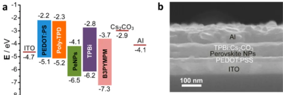
It is noted that the PLQE of the perovskite NPfilm is much higher than that of the bulkfilm. Generally, the exciton binding energy of the perovskite semiconductor reported in literature is several tens of millielectronvolts.13,14,38−41This implies that at room temperature excitons are partially ionized to free carriers. The free carriers in the bulk recombination layer would result in the low luminous efficiency and high leakage current of PeLED. However, the colloidal perovskite NP architecture would suppress the exciton dissociation effectively, leading to high quantum yield. As indicated in Figure 5a,b, the initial PeLED architecture in this work was designed as ITO/ PEDOT:PSS (40 nm)/perovskite NPs (40 nm)/TPBi (50 nm)/TPBi:Cs2CO3(10 wt %, 20 nm)/Al. The energy level of perovskite was measured using ultraviolet photoelectron spectroscopy (UPS,Figure S7). The PEDOT:PSSfilm worked as an ITO modification layer to enhance hole injection and the hole transport layer. Both the PEDOT:PSS and perovskite NP films were deposited onto the ITO substrate by spin-coating sequentially. As shown in the atomic force microscopy (AFM,
Figure S8) image, the surface roughness Ra of the perovskite film on PEDOT:PSS is only 4.35 nm, and such an excellent morphology satisfies the requirement of high-quality LEDs. The other functional films were deposited using vacuum thermal evaporation. To avoid electrical shunting paths caused by the contact between the perovskite NP layer and the cathode, which would cause a lower quantum yield, a 70 nm TPBi electron transport layer was employed as the conformal coating to separate the two layers completely. However, the low electron mobility of the TPBifilm may cause a higher driving voltage and imbalance charge carriers in the recombination zone; therefore, a 20 nm thick intrinsic TPBi layer on the cathode side was replaced by a 20 nm n-type-doped TPBi:Cs2CO3 layer, which can also enhance the film conductivity and electron injection from the Al cathode.
Above all, to optimize the device performance, the influence of different thicknesses of the perovskite NP film was investigated; as a result, the device with a 40 nm (1500 rpm) perovskite NPfilm showed the best overall performance (Table S2). The current density−voltage−luminance of the PeLED is shown in Figure 6a. The electroluminescence (EL) of the
PeLED is consistent with PL (Figure 6c). To confirm the Lambertian emission feature of the PeLED, we have measured the EL spectra with different view angles, and there is no noticeable shift or shape change with the angle change (Figure S9). A maximum brightness of 3515 cd/m2was achieved at a current density of 73.8 mA/cm2. A maximum power efficiency of 7.84 lm/W was obtained at 0.82 mA/cm2and 90.6 cd/m2. A
Figure 5. (a) Energy level diagram of different layers of the PeLED, showing the conduction and valence band levels with respect to vacuum. (b) Cross-sectional SEM image of the PeLED device.
Figure 6. (a) Current density−voltage (black) and luminance− voltage (red) characteristics. (b) Power efficiency−current density (black) and external quantum yield−current density (red) characteristics. (c) Electroluminescence spectra at a peak wave-length of 512 nm and with a fwhm of 26 nm, and the image of the resulting device operating at a luminance of 1189 cd/m2.
maximum EQE of 3.8% was obtained at 1.72 mA/cm2 and 198.1 cd/m2, which is 3.5 times higher than that with the best PeLED based on the perovskite NP colloid (Figure S10 and Table S4). Given the out-coupling efficiency of ∼20%, a maximum internal quantum efficiency (IQE) of 19% was achieved. As an emerging material, the reliability of perovskite NPs still needs to be improved; for example, even the devices with an identical structure presented somefluctuation in overall performance (devices 1−5, Table S3). Here, we obtained the champion value of the key parameters, such as the maximum luminance of 11 830 cd/m2in different devices (Table S3). The luminous efficiency of the PeLED rises initially and then drops with increasing current density, which is similar to the trend with previously reported results.15,32
Considering the enormous difference of conductivity between PEDOT:PSS film and amorphous TPBi film, the opposite charge carriers reached in the perovskite recombina-tion zone were probably imbalanced, which quenched the emission. In order to improve the device performance, we further optimized the PeLED. First, we added a poly-TPDfilm as a hole transport layer between the PEDOT:PSS and perovskite NP layer to balance the charge carriers in the recombination zone. We fabricated devices 5 and 6 using identical materials in a single run to compare the performance. As indicated inFigures S11 and S12, the poly-TPD layer can effectively improve the device performance drastically, includ-ing a higher EQE and a lower drivinclud-ing voltage. Furthermore, we fabricated one device in which half of the PEDOT:PSSfilm was covered by poly-TPD film. In such a device, significant enhanced emission from the half device with poly-TPD film was observed. Nonetheless, probably due to the just passable reliability, the performance of device with poly-TPD was still less than 3.8%.
As shown in Figure S13, the device presents a negative differential resistance effect at a driving current density of about 100 mA/cm2. As the luminance is a monotonically and approximately linearly increasing function of the driving current density, a higher brightness needs a higher driving current density to support. Therefore, we modified the device structure furthermore by replacing the electron transport layer of TPBi by B3PYMPM with higher electron mobility. As indicated in
Figure S14, device 7 can support a much higher driving current density. It is noted that in device 7, due to the high electron mobility of B3PYMPM, the driving voltage decreases substantially, allowing it to reach 1000 cd/m2 at only 3.9 V, which is helpful to achieve higher power efficiency. Similarly, the device with B3PYMPM also presented a dramatic fluctuation in overall device performance. Finally, we investigated the stability of the PeLED with the structure of ITO/PEDOT:PSS/perovskite NPs/TPBi/TPBi:Cs2CO3/Al. The lifetime of the device is about 30 s as the brightness decreases to 50% of the initial value of 100 cd/m2(Figure S15). The stability of the organometal halide perovskite-based devices (solar cell and LED) is a still a daunting problem that hinders the application of the perovskite, and there is a considerable margin to improve.
CONCLUSIONS
In summary, we have synthesized a series of colloidal organometal halide perovskite amorphous NPs by a facile solution method. The high-performance PeLEDs based on the colloidal organometal halide perovskite amorphous NPs have been demonstrated, and the high-efficiency LED shows a
maximum bright luminance and created a very high EQE of the green PeLED. Such high performance can be attributed to the excellent PLQE of the perovskite sample as well as their unique colloidal amorphous NP structure. Though the reliability still needs to be improved, our demonstration of efficient PeLED shows the feasibility and promising prospect in the application of surface-emitting LED based on colloidal organometal halide perovskite NPs.
METHODS
Perovskite NP Preparation. Methylamine (CH3NH2) solution in
ethanol was reacted with haloid acid (HI, HBr, or HCl) in water with excess methylamine at 0 °C. The precipitate was recovered via evaporation at 60 °C. The yellowish raw product was washed with diethyl etherfive times and dried at 60 °C in a vacuum oven for 24 h. For the synthesis of amorphous CH3NH3PbBr3 NPs, 0.225 mmol
methylamine bromide (CH3NH3Br) and 0.15 mmol lead bromide
(PbBr2) were dissolved in 0.5 mL of anhydrous DMF and 8.5 mL of
γ-butyrolactone mixed solution with 15 μL of octylamine to form a halide perovskite precursor solution (S-1). Next, 0.3 mL of the perovskite precursor solution was dropped into 5 mL of toluene with vigorous stirring. The colloidal solution was centrifuged at 5000 rpm for 5 min to discard the aggregated precipitates, and the perovskite NPs were obtained after being centrifuged at 15 000 rpm. For the other precursor solutions, S-2 to S-4, the concentrations of the CH3NH3Br and PbBr2are kept the same as above, but the volumes of
DMF,γ-butyrolactone, and octylamine change to 4.5 mL, 4.5 mL, 15 μL (S-2); 9 mL, 0 mL, 15 μL (S-3); and 0.5 mL, 8.5 mL, 0 μL (S-4). CH3NH3PbCl3 and CH3NH3PbI3 amorphous NPs were synthesized
by a similar method but with varying precursors and solvents. Dimethylsulfoxide and γ-butyrolactone mixed solution was used to dissolve the PbCl2 and CH3NH3Cl. The mixed perovskites
CH3NH3PbBrxI3−x and CH3NH3PbClxBr3−x were fabricated by
blending the perovskite precursor solution with an appropriate ratio. The perovskite NP product was dispersed in tetrahydrofuran to form the colloidal solution, with a concentration of 5 mg/mL for LED fabrication. The polycrystalline perovskitefilm was spin-coated on a quartz substrate from DMF solution with CH3NH3Br (0.1 M) and
PbBr2(0.1 M). The crystalline CH3NH3PbBr3NPs were synthesized
according to a previous report.6
Characterizations. The structure of as-grown samples was characterized using XRD (Bruker D8 Advanced diffractometer with Cu Kα radiation) and transmission electron microscopy with energy-dispersive X-ray spectroscopy (subangstrom resolution, aberration-corrected TITAN G2 60-300 and JEM 2100F). The colloid attribution was measured by DLS (Malvern Nano-ZS, measurement ranges from 0.3 nm to 10μm). UV−vis absorption was measured on a LAMBDA 950 UV/vis/NIR spectrophotometer, and PL spectra were taken using afluorescence spectrometer (Cary Eclipse). The absolute PL quantum efficiency was determined by a fluorescence spectrometer with an integrated sphere excited under 415 nm laser irradiation. The temperature-dependent PL spectra were measured with a micro-Raman spectrometer (Horiba-JY T64000) with a single-grating setup and 473 nm (solid-state laser) excitation laser. The backscattered signal was collected through a 50× (VIS) objective and recorded by a liquid-nitrogen-cooled charge-coupled device detector. The morphol-ogy and structure of the LED device were characterized by atomic force microscopy (Veeco Dimension V) in the tapping mode and field-emission scanning electron microscopy (JEOL JSM-7001F). UPS measurements were performed on the samples in a home-built UHV multichamber system with base pressure better than 1× 10⁻⁹Torr. The UPS source was a helium discharge lamp (hν = 21.2 eV). The photoelectrons were measured by an electron analyzer (Omicron EA125).
Time-Resolved Photoluminescence Spectroscopy. The ex-citation pulse (400 nm) was generated by frequency doubling the 800 nm output with a BBO crystal from the MaiTai (SpectraPhysics) (∼100 fs, 80 MHz, 800 nm). The pump laser source was introduced into a microscope (Nikon ECLIPSE Ti−U) and focused onto samples
with a 100× objective (Nikon, numerical aperture: 0.9). To obtain sufficient energy injection, the laser spot was focused to the diffraction limit. The reflected emission was collected by the same objective. The emission was time-resolved using a PicoHarp 300 system, and the data were analyzed with SymPhoTime 64 (PicoQuant).
Device Fabrication and Characterizations. All chemicals used in this work are commercially available. Patterned indium tin oxide (ITO) glass substrates (10Ω/sq) were cleaned with deionized water, isopropyl alcohol, and acetone in sequence and then oven-dried and treated in O2 plasma. A 40 nm PEDOT:PSS layer was spun on the
ITO substrate at 4000 rpm for 60 s and then annealed at 150°C for 30 min in the ambient air. All samples were transferred into a N2
atmosphere glovebox for the deposition of a 40 nm poly(4-butylphenyl diphenylamine) (poly-TPD) film by spin-coating at 2500 rpm for 60 s and then annealing at 150°C for 30 min; then the perovskite NP layer was spun onto the substrates at 1500 rpm for 60 s. The 3,5-tris(1-phenyl-1H-benzimidazol-2-yl)benzene (TPBi), 4,6-bis(3,5-di(pyridin-3-yl)phenyl)-2-methylpyrimidine, and 4,6-bis-(3,5-di-3-pyridylphenyl)-2-methylpyrimidine (B3PYMPM) served as the electron transport layers (ETL); the ETL doped with cesium carbonate (Cs2CO3) worked as the electron injection layer, and the
aluminum electrodes were fabricated by thermal evaporation in a single run at a base pressure of less than 3× 10⁻⁴Pa without breaking the vacuum. All organics and other compounds were evaporated at a rate of about 0.1 nm s−1, and the aluminum electrodes were evaporated at a rate of 0.8−1 nm s−1. A shadow mask was used to
define the cathode, and we could obtain six devices (with an emissive area of 1× 1 mm2) on each substrate. All devices were encapsulated by
UV glue and glass cover in a N2 atmosphere glovebox for the
characterization operated in ambient air. The luminance−current− voltage (L−I−V) characteristics and electroluminescence spectra were measured simultaneously with an Agilent B2902A source meter and Konica Minolta LS-110 luminance meter. The electroluminescence spectra were measured using a PR705 spectrometer. The maximum EQE was limited by the light out-coupling efficiency of the device, which can be estimated from ηout = 1/(2n2) for layer-by-layer
structures without out-coupling enhancement instruments, where n is the refractive index of the organic material and assuming n = 1.5.ηoutis
typically around 20%.
ASSOCIATED CONTENT
*
S Supporting InformationThe Supporting Information is available free of charge on the
ACS Publications websiteat DOI:10.1021/acsnano.6b01540. Additional TEM, AFM, TRPL, PLQE analysis, and LED performances (PDF)
AUTHOR INFORMATION
Corresponding Author
*Email:[email protected].
Notes
The authors declare no competingfinancial interest.
ACKNOWLEDGMENTS
Q.H.X. gratefully acknowledges financial support from Singapore National Foundation via an Investigatorship Award (NRF-NRFI2015-03) and a Competitive Research Program (NRF-CRP-6-2010-2), and Singapore Ministry of Education through two AcRF Tier2 grants (MOE2011-T2-2-051 and MOE2015-T2-1-047). H.V.D. gratefully acknowledgesfinancial support from Singapore National Foundation NRF-CRP-6-2010-02, A*STAR of Singapore, and TUBA.
REFERENCES
(1) Yang, W. S.; Noh, J. H.; Jeon, N. J.; Kim, Y. C.; Ryu, S.; Seo, J.; Seok, S. I. High−Performance Photovoltaic Perovskite Layers
Fabricated through Intramolecular Exchange. Science 2015, 348, 1234−1237.
(2) Stranks, S. D.; Snaith, H. J. Metal−Halide Perovskites for Photovoltaic and Light−Emitting Devices. Nat. Nanotechnol. 2015, 10, 391−402.
(3) Shockley, W.; Queisser, H. J. Detailed Balance Limit of Efficiency of P−N Junction Solar Cells. J. Appl. Phys. 1961, 32, 510−519.
(4) Miller, O. D.; Yablonovitch, E.; Kurtz, S. R. Strong Internal and External Luminescence as Solar Cells Approach the Shockley− Queisser Limit. IEEE J. Photovoltaics 2012, 2, 303−311.
(5) Schmidt, L. C.; Pertegás, A.; González-Carrero, S.; Malinkiewicz, O.; Agouram, S.; Mínguez Espallargas, G.; Bolink, H. J.; Galian, R. E.; Pérez-Prieto, J. Nontemplate Synthesis of CH3NH3PbBr3 Perovskite
Nanoparticles. J. Am. Chem. Soc. 2014, 136, 850−853.
(6) Zhang, F.; Zhong, H.; Chen, C.; Wu, X.−G.; Hu, X.; Huang, H.; Han, J.; Zou, B.; Dong, Y. Brightly Luminescent and Color−Tunable Colloidal CH3NH3PbX3 (X = Br, I, Cl) Quantum Dots: Potential
Alternatives for Display Technology. ACS Nano 2015, 9, 4533−4542. (7) Huang, H.; Susha, A. S.; Kershaw, S. V.; Hung, T. F.; Rogach, A. L. Control of Emission Color of High Quantum Yield CH3NH3PbBr3
Perovskite Quantum Dots by Precipitation Temperature. Adv. Science 2015, 2, 1500194.
(8) Gonzalez-Carrero, S.; Galian, R. E.; Perez-Prieto, J. Maximizing The Emissive Properties of CH3NH3PbBr3Perovskite Nanoparticles. J.
Mater. Chem. A 2015, 3, 9187−9193.
(9) Stoumpos, C. C.; Malliakas, C. D.; Kanatzidis, M. G. Semiconducting Tin and Lead Iodide Perovskites with Organic Cations: Phase Transitions, High Mobilities, and Near−Infrared Photoluminescent Properties. Inorg. Chem. 2013, 52, 9019−9038.
(10) Baikie, T.; Fang, Y.; Kadro, J. M.; Schreyer, M.; Wei, F.; Mhaisalkar, S. G.; Graetzel, M.; White, T. J. Synthesis and Crystal Chemistry of the Hybrid Perovskite (CH3NH3)PbI3 for Solid−State
Sensitised Solar Cell Applications. J. Mater. Chem. A 2013, 1, 5628− 5641.
(11) Xing, J.; Liu, X. F.; Zhang, Q.; Ha, S. T.; Yuan, Y. W.; Shen, C.; Sum, T. C.; Xiong, Q. H. Vapor Phase Synthesis of Organometal Halide Perovskite Nanowires for Tunable Room−Temperature Nanolasers. Nano Lett. 2015, 15, 4571−4577.
(12) Zhang, Q.; Ha, S. T.; Liu, X.; Sum, T. C.; Xiong, Q. H. Room− Temperature Near−Infrared High−Q Perovskite Whispering−Gallery Planar Nanolasers. Nano Lett. 2014, 14, 5995−6001.
(13) D’Innocenzo, V.; Grancini, G.; Alcocer, M. J. P.; Kandada, A. R. S.; Stranks, S. D.; Lee, M. M.; Lanzani, G.; Snaith, H. J.; Petrozza, A. Excitons versus Free Charges in Organo−Lead Tri−Halide Perov-skites. Nat. Commun. 2014, 5, 3586.
(14) Tanaka, K.; Takahashi, T.; Ban, T.; Kondo, T.; Uchida, K.; Miura, N. Comparative Study on the Excitons in Lead−Halide−Based Perovskite−Type Crystals CH3NH3PbBr3 CH3NH3PbI3. Solid State
Commun. 2003, 127, 619−623.
(15) Tan, Z.−K.; Moghaddam, R. S.; Lai, M. L.; Docampo, P.; Higler, R.; Deschler, F.; Price, M.; Sadhanala, A.; Pazos, L. M.; Credgington, D.; et al. Bright Light−Emitting Diodes Based on Organometal Halide Perovskite. Nat. Nanotechnol. 2014, 9, 687−692.
(16) Wang, J.; Wang, N.; Jin, Y.; Si, J.; Tan, Z.−K.; Du, H.; Cheng, L.; Dai, X.; Bai, S.; He, H.; et al. Interfacial Control Toward Efficient and Low−Voltage Perovskite Light−Emitting Diodes. Adv. Mater. 2015, 27, 2311−2316.
(17) Kim, Y.−H.; Cho, H.; Heo, J. H.; Kim, T.−S.; Myoung, N.; Lee, C.−L.; Im, S. H.; Lee, T.−W. Multicolored Organic/Inorganic Hybrid Perovskite Light−Emitting Diodes. Adv. Mater. 2015, 27, 1248−1254. (18) Hoye, R. L. Z.; Chua, M. R.; Musselman, K. P.; Li, G.; Lai, M.− L.; Tan, Z.−K.; Greenham, N. C.; MacManus-Driscoll, J. L.; Friend, R. H.; Credgington, D. Enhanced Performance in Fluorene−Free Organometal Halide Perovskite Light−Emitting Diodes Using Tunable, Low Electron Affinity Oxide Electron Injectors. Adv. Mater. 2015, 27, 1414−1419.
(19) Li, G.; Tan, Z.−K.; Di, D.; Lai, M. L.; Jiang, L.; Lim, J. H.−W.; Friend, R. H.; Greenham, N. C. Efficient Light−Emitting Diodes
Based on Nanocrystalline Perovskite in a Dielectric Polymer Matrix. Nano Lett. 2015, 15, 2640−2644.
(20) Jaramillo-Quintero, O. A.; Sanchez, R. S.; Rincon, M.; Mora-Sero, I. Bright Visible−Infrared Light Emitting Diodes Based on Hybrid Halide Perovskite with Spiro−OMeTAD as a Hole−Injecting Layer. J. Phys. Chem. Lett. 2015, 6, 1883−1890.
(21) Kumawat, N. K.; Dey, A.; Narasimhan, K. L.; Kabra, D. Near Infrared to Visible Electroluminescent Diodes Based on Organo-metallic Halide Perovskites: Structural and Optical Investigation. ACS Photonics 2015, 2, 349−354.
(22) Sadhanala, A.; Ahmad, S.; Zhao, B.; Giesbrecht, N.; Pearce, P. M.; Deschler, F.; Hoye, R. L. Z.; Gödel, K. C.; Bein, T.; Docampo, P.; et al. Blue−Green Color Tunable Solution Processable Organolead Chloride−Bromide Mixed Halide Perovskites for Optoelectronic Applications. Nano Lett. 2015, 15, 6095−6101.
(23) Yu, J. C.; Kim, D. B.; Baek, G.; Lee, B. R.; Jung, E. D.; Lee, S.; Chu, J. H.; Lee, D.−K.; Choi, K. J.; Cho, S.; et al. High−Performance Planar Perovskite Optoelectronic Devices: A Morphological and Interfacial Control by Polar Solvent Treatment. Adv. Mater. 2015, 27, 3492−3500.
(24) Bade, S. G. R.; Li, J.; Shan, X.; Ling, Y.; Tian, Y.; Dilbeck, T.; Besara, T.; Geske, T.; Gao, H.; Ma, B.; et al. Fully Printed Halide Perovskite Light−Emitting Diodes with Silver Nanowire Electrodes. ACS Nano 2016, 10, 1795−1801.
(25) Dai, X.; Zhang, Z.; Jin, Y.; Niu, Y.; Cao, H.; Liang, X.; Chen, L.; Wang, J.; Peng, X. Solution−Processed, High−Performance Light− Emitting Diodes Based on Quantum Dots. Nature 2014, 515, 96−99. (26) Muller, C. D.; Falcou, A.; Reckefuss, N.; Rojahn, M.; Wiederhirn, V.; Rudati, P.; Frohne, H.; Nuyken, O.; Becker, H.; Meerholz, K. Multi−Colour Organic Light−Emitting Displays by Solution Processing. Nature 2003, 421, 829−833.
(27) Dodabalapur, A. Organic Light Emitting Diodes. Solid State Commun. 1997, 102, 259−267.
(28) Greenham, N. C.; Moratti, S. C.; Bradley, D. D. C.; Friend, R. H.; Holmes, A. B. Efficient Light−Emitting Diodes Based on Polymers with High Electron Affinities. Nature 1993, 365, 628−630.
(29) Colvin, V. L.; Schlamp, M. C.; Alivisatos, A. P. Light−Emitting Diodes Made from Cadmium Selenide Nanocrystals and a Semi-conducting Polymer. Nature 1994, 370, 354−357.
(30) Coe, S.; Woo, W.−K.; Bawendi, M.; Bulovic, V. Electro-luminescence from Single Monolayers of Nanocrystals in Molecular Organic Devices. Nature 2002, 420, 800−803.
(31) Demir, H. V.; Seker, U. O. S.; Zengin, G.; Mutlugun, E.; Sari, E.; Tamerler, C.; Sarikaya, M. Spatially Selective Assembly of Quantum Dot Light Emitters in an LED Using Engineered Peptides. ACS Nano 2011, 5, 2735−2741.
(32) Yan, F.; Chen, R.; Sun, H.; Sun, X. W. Organic Light−Emitting Diodes with a Spacer Enhanced Exciplex Emission. Appl. Phys. Lett. 2014, 104, 153302.
(33) Cho, H.; Jeong, S.−H.; Park, M.−H.; Kim, Y.−H.; Wolf, C.; Lee, C.−L.; Heo, J. H.; Sadhanala, A.; Myoung, N.; Yoo, S.; et al. Overcoming the Electroluminescence Efficiency Limitations of Perovskite Light−Emitting Diodes. Science 2015, 350, 1222−1225.
(34) Li, X.; Wu, Y.; Zhang, S.; Cai, B.; Gu, Y.; Song, J.; Zeng, H. CsPbX3 Quantum Dots for Lighting and Displays:
Room−Temper-ature Synthesis, Photoluminescence Superiorities, Underlying Origins and White Light−Emitting Diodes. Adv. Funct. Mater. 2016, 26, 2435− 2445.
(35) Yan, K.; Long, M.; Zhang, T.; Wei, Z.; Chen, H.; Yang, S.; Xu, J. Hybrid Halide Perovskite Solar Cell Precursors: Colloidal Chemistry and Coordination Engineering behind Device Processing for High Efficiency. J. Am. Chem. Soc. 2015, 137, 4460−4468.
(36) Poglitsch, A.; Weber, D. Dynamic Disorder in Methylammo-niumtrihalogenoplumbates (II) Observed by Millimeter−Wave Spec-troscopy. J. Chem. Phys. 1987, 87, 6373−6378.
(37) Wang, Y.; Gould, T.; Dobson, J. F.; Zhang, H.; Yang, H.; Yao, X.; Zhao, H. Density Functional Theory Analysis of Structural and Electronic Properties of Orthorhombic Perovskite CH3NH3PbI3. Phys.
Chem. Chem. Phys. 2014, 16, 1424−1429.
(38) Miyata, A.; Mitioglu, A.; Plochocka, P.; Portugall, O.; Wang, J. T.−W.; Stranks, S. D.; Snaith, H. J.; Nicholas, R. J. Direct Measurement of the Exciton Binding Energy and Effective Masses for Charge Carriers in Organic−Inorganic Tri−Halide Perovskites. Nat. Phys. 2015, 11, 582−587.
(39) Lin, Q.; Armin, A.; Nagiri, R. C. R.; Burn, P. L.; Meredith, P. Electro−Optics of Perovskite Solar Cells. Nat. Photonics 2015, 9, 106− 112.
(40) Wu, K.; Bera, A.; Ma, C.; Du, Y.; Yang, Y.; Li, L.; Wu, T. Temperature−Dependent Excitonic Photoluminescence of Hybrid Organometal Halide Perovskite Films. Phys. Chem. Chem. Phys. 2014, 16, 22476−22481.
(41) Savenije, T. J.; Ponseca, C. S.; Kunneman, L.; Abdellah, M.; Zheng, K.; Tian, Y.; Zhu, Q.; Canton, S. E.; Scheblykin, I. G.; Pullerits, T.; et al. Thermally Activated Exciton Dissociation and Recombination Control the Carrier Dynamics in Organometal Halide Perovskite. J. Phys. Chem. Lett. 2014, 5, 2189−2194.