Virginia Commonwealth University
VCU Scholars Compass
Electrical and Computer Engineering Publications
Dept. of Electrical and Computer Engineering
2003
4H–SiC photoconductive switching devices for
use in high-power applications
S. Doǧan
Virginia Commonwealth University
A. Teke
Virginia Commonwealth University
D. Huang
Virginia Commonwealth University See next page for additional authors
Follow this and additional works at:
http://scholarscompass.vcu.edu/egre_pubs
Part of the
Electrical and Computer Engineering Commons
Doǧan, S., Teke, A., Huang, D., et al. 4H–SiC photoconductive switching devices for use in high-power applications. Applied Physics Letters, 82, 3107 (2003). Copyright © 2003 AIP Publishing LLC.
This Article is brought to you for free and open access by the Dept. of Electrical and Computer Engineering at VCU Scholars Compass. It has been accepted for inclusion in Electrical and Computer Engineering Publications by an authorized administrator of VCU Scholars Compass. For more information, please [email protected].
Downloaded from
Authors
S. Doǧan, A. Teke, D. Huang, Hadis Morkoç, C. B. Roberts, J. Parish, B. Ganguly, M. Smith, R. E. Meyers, and
S. E. Saddow
4H–SiC photoconductive switching devices for use in high-power
applications
S. Dogˇan,a)A. Teke,b)D. Huang, and H. Morkoc¸
Department of Electrical Engineering, Virginia Commonwealth University, 601 W. Main Street, Richmond, Virginia 23284
C. B. Roberts
Tech Explore, Limited Liability Corporation, 5273 College Corner Pike No. 12, Oxford, Ohio 45056
J. Parish and B. Ganguly
Air Force Research Laboratory, Wright–Patterson Air Force Base, Ohio 45433
M. Smith, R. E. Myers, and S. E. Saddow
Electrical Engineering University of South Florida, Tampa, Florida 33543
共Received 12 December 2002; accepted 10 March 2003兲
Silicon carbide is a wide-band-gap semiconductor suitable for high-power high-voltage devices and it has excellent properties for use in photoconductive semiconductor switches共PCSSs兲. PCSS were fabricated as planar structures on high-resistivity 4H–SiC and tested at dc bias voltages up to 1000 V. The typical maximum photocurrent of the device at 1000 V was about 49.4 A. The average on-state resistance and the ratio of on-state to off-state currents were about 20 ⍀ and 3⫻1011, respectively. Photoconductivity pulse widths for all applied voltages were 8 –10 ns. These excellent results are due in part to the removal of the surface damage by high-temperature H2 etching and surface preparation. Atomic force microscopy images revealed that very good surface morphology, atomic layer flatness, and large step width were achieved. © 2003 American Institute of Physics.
关DOI: 10.1063/1.1571667兴
Silicon carbide共SiC兲, a wide-band-gap semiconductor of
⬃3 eV, is a candidate material for electronic and optical
devices and has advantages over other semiconductors espe-cially for high-frequency, high-temperatures and high-power applications.1 This is because of its high saturation electron
velocity (2.0⫻107 cm/s), thermal conductivity
(4.9 W/cm °C), and high breakdown field共4 MV/cm兲.2,3The large band gap and high saturation electron velocity of SiC provide excellent temperature stability and high-frequency performance for various device applications.4 For that reason, SiC technology has made tremendous improve-ments in the last decade with a variety of encouraging device and circuit demonstrations.5
SiC-based semiconductor electronic devices and circuits are presently being developed for use in power, high-temperature, and high radiation conditions in which conven-tional semiconductors can not adequately perform. The pho-toconductive semiconductor switch 共PCSS兲 is an important type of electronic device and excels in applications requiring high voltage and high speed. Some of the applications of the PCSS include high-speed photodetectors, high-voltage pulse generation, and electron-beam pumped lasers, and radio fre-quency interference immunity. There is strong interest in de-veloping these devices for use in power and high-temperature applications. PCSSs have unique advantages over conventional power switches including high breakdown
field, high speed, long lifetime, and negligible jitter time. Although Si and GaAs are the most commonly used materi-als in PCSS,6,7compared to GaAs and Si, better performance and wider 共more兲 applications are expected from SiC PCSS due to its higher saturation electron drift velocity and higher thermal conductivity. The advantages of PCSSs over conven-tional switches make them the perfect choice for many im-portant applications where high switching accuracy and power capability are important. Furthermore, wide-band-gap semiconductor switches are attractive since they have a higher tolerance compared to other switches due to their bet-ter mabet-terial properties. There has been significant inbet-terest in using high-resistivity SiC, among the wide-band-gap semi-conductors, for PCSS because it is one of the most techno-logically advanced materials.8 –10 In addition, PCSSs have been fabricated on SiC, both on 6H–SiC 共Refs. 9 and 11兲 and later on 3C–SiC.12 However, a lack of semi-insulating substrates prevented further development of PCSS technol-ogy on SiC due to the high dark currents normally encoun-tered with less resistive substrates.
In this letter, we report measurements on 4H–SiC PCSSs for high-voltage applications. The devices were fabricated on bulk polycrystalline SiC material. These results are comple-mented by photoconductivity measurements under a large dc bias.
The devices were fabricated with a circular geometry with a switching gap of 1 mm on high-resistivity 4H–SiC. This relatively large device size was chosen to prevent arcing at high voltages, since the dielectric breakdown field strength of air is approximately 30 kV/cm. Since the fabricated de-vices are planar, the majority of the conduction will be along
a兲Also with Atatu¨rk University, Faculty of Arts and Sciences, Dept. of
Phys-ics, 25240 Erzurum, Turkey; electronic mail: [email protected]
b兲Also with Balikesir University, Faculty of Arts and Sciences, Dept. of
Physics, 10100 Balikesir, Turkey.
APPLIED PHYSICS LETTERS VOLUME 82, NUMBER 18 5 MAY 2003
3107
0003-6951/2003/82(18)/3107/3/$20.00 © 2003 American Institute of Physics
This article is copyrighted as indicated in the article. Reuse of AIP content is subject to the terms at: http://scitation.aip.org/termsconditions. Downloaded to IP: 128.172.48.58 On: Tue, 21 Apr 2015 18:00:04
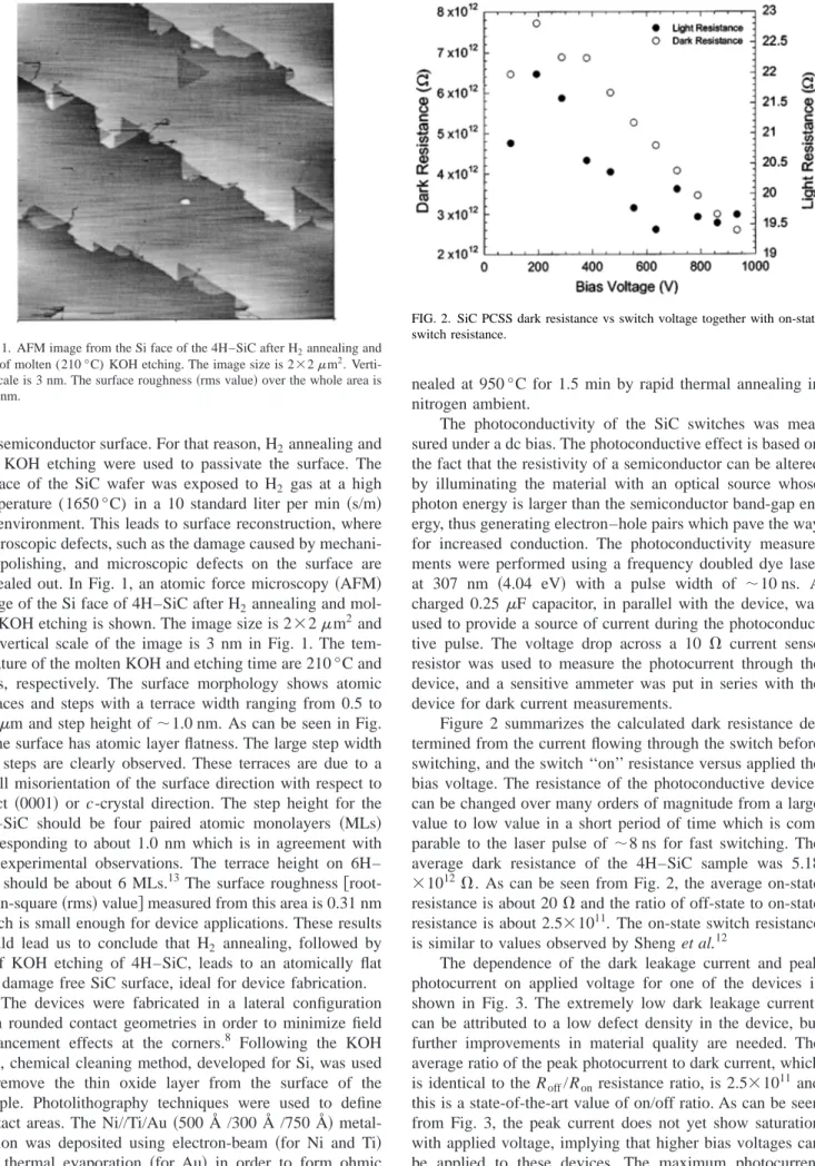
the semiconductor surface. For that reason, H2annealing and wet KOH etching were used to passivate the surface. The surface of the SiC wafer was exposed to H2 gas at a high temperature (1650 °C) in a 10 standard liter per min 共s/m兲 H2 environment. This leads to surface reconstruction, where macroscopic defects, such as the damage caused by mechani-cal polishing, and microscopic defects on the surface are annealed out. In Fig. 1, an atomic force microscopy共AFM兲 image of the Si face of 4H–SiC after H2 annealing and mol-ten KOH etching is shown. The image size is 2⫻2m2 and the vertical scale of the image is 3 nm in Fig. 1. The tem-perature of the molten KOH and etching time are 210 °C and 15 s, respectively. The surface morphology shows atomic terraces and steps with a terrace width ranging from 0.5 to 0.8m and step height of⬃1.0 nm. As can be seen in Fig. 1, the surface has atomic layer flatness. The large step width and steps are clearly observed. These terraces are due to a small misorientation of the surface direction with respect to exact 共0001兲 or c-crystal direction. The step height for the 4H–SiC should be four paired atomic monolayers 共MLs兲 corresponding to about 1.0 nm which is in agreement with the experimental observations. The terrace height on 6H– SiC should be about 6 MLs.13The surface roughness 关root-mean-square共rms兲 value兴 measured from this area is 0.31 nm which is small enough for device applications. These results would lead us to conclude that H2 annealing, followed by brief KOH etching of 4H–SiC, leads to an atomically flat and damage free SiC surface, ideal for device fabrication.
The devices were fabricated in a lateral configuration with rounded contact geometries in order to minimize field enhancement effects at the corners.8 Following the KOH etch, chemical cleaning method, developed for Si, was used to remove the thin oxide layer from the surface of the sample. Photolithography techniques were used to define contact areas. The Ni//Ti/Au 共500 Å /300 Å /750 Å兲 metal-ization was deposited using electron-beam 共for Ni and Ti兲 and thermal evaporation 共for Au兲 in order to form ohmic contacts. A standard lift-off process was applied in acetone to transfer the pattern to the sample. The contacts were
an-nealed at 950 °C for 1.5 min by rapid thermal annealing in nitrogen ambient.
The photoconductivity of the SiC switches was mea-sured under a dc bias. The photoconductive effect is based on the fact that the resistivity of a semiconductor can be altered by illuminating the material with an optical source whose photon energy is larger than the semiconductor band-gap en-ergy, thus generating electron–hole pairs which pave the way for increased conduction. The photoconductivity measure-ments were performed using a frequency doubled dye laser at 307 nm 共4.04 eV兲 with a pulse width of ⬃10 ns. A charged 0.25 F capacitor, in parallel with the device, was used to provide a source of current during the photoconduc-tive pulse. The voltage drop across a 10 ⍀ current sense resistor was used to measure the photocurrent through the device, and a sensitive ammeter was put in series with the device for dark current measurements.
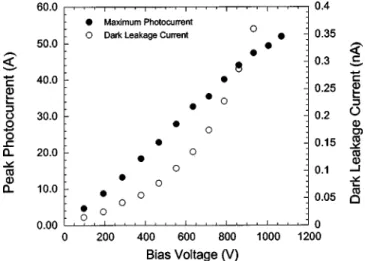
Figure 2 summarizes the calculated dark resistance de-termined from the current flowing through the switch before switching, and the switch ‘‘on’’ resistance versus applied the bias voltage. The resistance of the photoconductive devices can be changed over many orders of magnitude from a large value to low value in a short period of time which is com-parable to the laser pulse of ⬃8 ns for fast switching. The average dark resistance of the 4H–SiC sample was 5.18
⫻1012 ⍀. As can be seen from Fig. 2, the average on-state resistance is about 20⍀ and the ratio of off-state to on-state resistance is about 2.5⫻1011. The on-state switch resistance is similar to values observed by Sheng et al.12
The dependence of the dark leakage current and peak photocurrent on applied voltage for one of the devices is shown in Fig. 3. The extremely low dark leakage currents can be attributed to a low defect density in the device, but further improvements in material quality are needed. The average ratio of the peak photocurrent to dark current, which is identical to the Roff/Ronresistance ratio, is 2.5⫻1011 and this is a state-of-the-art value of on/off ratio. As can be seen from Fig. 3, the peak current does not yet show saturation with applied voltage, implying that higher bias voltages can be applied to these devices. The maximum photocurrent measured at 1000 V was 49.4 A. Figure 4 summarizes the dependence of peak photocurrent on incident laser power at
FIG. 1. AFM image from the Si face of the 4H–SiC after H2annealing and
15 s of molten (210 °C) KOH etching. The image size is 2⫻2m2.
Verti-cal sVerti-cale is 3 nm. The surface roughness共rms value兲 over the whole area is 0.31 nm.
FIG. 2. SiC PCSS dark resistance vs switch voltage together with on-state switch resistance.
3108 Appl. Phys. Lett., Vol. 82, No. 18, 5 May 2003 Dogˇanet al.
This article is copyrighted as indicated in the article. Reuse of AIP content is subject to the terms at: http://scitation.aip.org/termsconditions. Downloaded to IP: 128.172.48.58 On: Tue, 21 Apr 2015 18:00:04
1005 V. The beam was attenuated, and its power measured, as each of a series of glass microscope slides were placed in the beam path. The photoconductivity experiments were then repeated with these calibrated decreases in laser pulse en-ergy. As is seen from the inset of Fig. 4, the photocurrent saturates with increasing excitation intensity. The contact separation of the current device is 1 mm and maximum ap-plied field is around 10 kV/cm. Since the drift velocity is about 106 cm/s at this value of field, the carrier transit time is about 10⫺7s. On the other hand, the longest free carrier lifetime in SiC is attainable only in high-quality SiC layers.14 If we assume that the carrier lifetime in our bulk material were the same as in high-quality SiC, we arrive at a photo-electronic gain of about 10⫺1 which is low. It is most likely that the carrier lifetime in our bulk sample is shorter due to the density of defects, which would lower the gain even fur-ther.
The output from a commercial frequency doubled dye
laser was used to measure the photoconductivity response of the PCSS. High breakdown voltage values corresponding to a high electric field have been achieved only for devices having a smaller area15and shorter gap distance8than those studied here. The electric field applied to the devices was calculated by dividing the applied voltage with the distance between contacts and was about 10 kV/cm. When the switch is illuminated, its photoconductivity will increase and current will start to flow through the current sense resistor, which gives us the observed photoconductivity response. The cur-rent should increase with increasing applied voltage until the saturation voltage is reached. The 4H–SiC PCSS tested switched the current many thousands of times and no degra-dation was shown on these devices at high voltage. No breakdown was observed on these devices meaning they can likely tolerate higher voltages and switch higher currents. In order to examine the high electric-field effects, switches fab-ricated with a small gap size should be used to reduce the effect of micropipes.16
In conclusion, planar PCSS have been fabricated on high-resistivity 4H–SiC in large sized structures. Photocon-ductivity measurements were done on these samples at bias voltages up to 1005 V. The average on-state resistance was 20⍀ and the average off-state resistance was 5⫻1012 ⍀, for an on/off ratio of 2.5⫻1011. The AFM image showed good surface morphology, atomic layer flatness, and large step width. The PCSS were measured with dc bias and showed repeatable behavior over many thousands of pulses.
This work was performed under USAF SBIR Contract No. F33615-02-M-2250 and benefited from programs at VCU from AFOSR, ONR, and NSF.
1
S. Nakashima, H. Matsunami, S. Yoshida, and H. Harima, Silicon Carbide
and Related Materials, 1995, Institute of Physics Conference Series No.
142共IOP, Bristol, 1996兲.
2Properties of Advanced Semiconductor Materials, edited by M. E.
Levin-shtein, S. L. Rumyantsev, and M. S. Shur共Wiley, New York, 2001兲.
3
P. G. Neudeck, Institute of Physics Conference Series 141, San Diego, CA, 1994, pp. 1– 6.
4J. W. Palmour, C. H. Carter, C. E. Weitzel, and K. J. Nordquist, Mater.
Res. Soc. Symp. Proc. 339, 133共1994兲.
5
R. R. Siergiej, R. C. Clarke, S. Sriram, A. K. Agarwal, R. J. Bojko, A. W. Morse, V. Balakrishna, M. F. Macmillan, A. A. Burk, and C. D. Brandt, Mater. Sci. Eng., B 61, 9共1999兲.
6High Power Optically Activated Solid-State Switches, edited by A. Rosen
and F. Zutavern共Artech House, Boston, 1994兲.
7
N. E. Islam, E. Schumiloglu, and C. B. Fleddermann, Appl. Phys. Lett. 73, 1988共1998兲.
8T. S. Sudarshan, G. Gradinaru, G. Korony, W. Mitchel, and R. H. Hopkins,
Appl. Phys. Lett. 67, 3435共1995兲.
9
P. S. Cho, J. Goldhar, C. H. Lee, S. E. Saddow, and P. Neudeck, J. Appl. Phys. 77, 1591共1995兲.
10S. E. Saddow, P. S. Cho, J. Goldhar, J. Palmour, and Chi H. Lee, Proc.
SPIE 1873, 110共1993兲.
11
S. E. Saddow, P. S. Cho, J. Goldhar, F. Barry McLean, J. W. Palmour, and C. H. Lee, Inst. Phys. Conf. Ser. 137, 573共1994兲.
12S. Sheng, M. G. Spencer, X. Tang, P. Zhou, K. Wongchotigul, C. Taylor,
and G. L. Harris, Mater. Sci. Eng., B 46, 147共1997兲.
13N. Onojima, J. Suda, and H. Matsunami, Appl. Phys. Lett. 80, 76共2001兲. 14
O. Kordina, P. Bergman, C. Hallin, and E. Janzen, Appl. Phys. Lett. 69, 679共1996兲.
15V. E. Chelnokov, A. L. Syrkin, and V. A. Dmitriev, Diamond Relat. Mater.
6, 1480共1997兲.
16G. Gradinaru and T. S. Sudarshan, J. Appl. Phys. 73, 7643共1993兲. FIG. 3. The dependence of peak photocurrent and leakage current of a
PCSS on applied voltage.
FIG. 4. Variation of photocurrent pulses with laser pulse energy. Inset shows the saturation of peak photocurrent with increasing laser pulse energy.
3109 Appl. Phys. Lett., Vol. 82, No. 18, 5 May 2003 Dogˇanet al.
This article is copyrighted as indicated in the article. Reuse of AIP content is subject to the terms at: http://scitation.aip.org/termsconditions. Downloaded to IP: 128.172.48.58 On: Tue, 21 Apr 2015 18:00:04