f ' ΐ ' . , ν , .'‘. i . , ^ , ,·.-> ; · ^ ^ '■ . · 4 > / ^ · Γ · · ; ^ . '·■· j : · }< > \j-,'^ X P y ,,¿ ,;;'::''1\- ;iS’'/--'::í·· i ''-i·;·.·, Λ-· ί . ' - · ' - г / . / ' . л ., ,;.';:",v,·-■ ' ';* · ■ ,■-·-., -■■•л·.'..;·,-^ " ч, " ^ ^ и <"* »' *. ·· -V--' ^ Í \'''''' ^ ^ ' -л ^ * ' ’■ ^ ^ "/ ν’#^''·’'·ίΝ>Λί;ν- . Xtf^* ,^-'Ч № «п' »· ■ .· ) -а .-;■ ,*^ίίν·.Γ .. .' · .. ..·.·«■ ..> ·.· ···.·:. .» . ; . ί · Λ . , - f · : · ' ΐ . -I ■ -I . . V : kl »i t..> a · ·'·> 4 . . ''V.. ♦ S і»· ·>'.J Λ .'·· .M w .J 1.-^·.« ui w i v; '\'.V ^*é M U ' wi, t í u -^ >, :'■ :і:нг-Г?^^71;I O ? С Г З© |5^В Е аШ © А Г Э aQSESM^ 'Гіл : a 3aüa:’j . L ^ L ä i : ' 3 T ' ^ a ·■'з т ж ^ ш ^ ш . . і / ■·. г , с . ■, .,: ,J („,- . <.^'Ä .і,;івіі »'.«'i)» ■· ■ , І'Іа гзу й і Y%3ft -,-,Λ í. 'ΐ:·:,γΐ
SUBMITTED TO THE DEPARTMENT OF PHYSICS AND THE INSTITUTE OF ENGINEERING AND SCIENCE
OF BILKENT UNIVERSITY
IN PARTIAL FULFILLMENT OF THE REQUIREMENTS FOR THE DEGREE OF
MASTER OF SCIENCE
By
'A ugust <997
opinion it is fully cidequate, in scope and in quality, as a dissertation for the degree of Master of Science.
I certify that I have read this thesis and that in rny opinion it is fully adequate, in scope and in qiuility, as a dissertation for the degree of Master of Science.
erpengiizel
Approved for the Institute of Engineering and Science:
Prof. Mehmet
GAAS/ALGAAS POLARIZATION SPLITTING
DIRECTIONAL COUPLERS
Nasuhi Yurt
M. S. in Physics
Supervisor: Prof. Dr. Atilla Aydınlı
August 1997
D irectional couplers are building blocks for m any guided wave devices in integrated optics and optoelectronics. Th ey have been used as switches, m odulators, w avelength filters, power dividers, wavelength m ultiplexer-dem ultiplexers, and are im p o rtan t com ponents for fu tu re switching networks. T h e ability to control polarization allows fu rth e r flexibility in integration o f optoelectronic com ponents. In this thesis, we present our w ork on th e design, fabrication and characterization o f G a A s /A IG a A s polarization splitting directional couplers. W e have designed a directional coupler o perating at 1.55 ¡.tm wavelength using a G aA s /A IG a A s heterostructure, th a t have different coupling lengths for T E and T M polarized guided modes. T h e device passively separates th e T E and T M polarized guided modes entering th e device at th e sam e input port, at th e o u tp u t ports. M e tal electrodes placed on th e waveguides allowed fo r control o f polarization.
Keywords: Directional couplers, polarization splitters, guided wave devices, G a A s /A IG a A s double heterostructure, coupled m ode theory, effective index calculations for couplers.
Ağustos 1997
Doğrusal çiftleyiciler tü m lenm iş optik ve opto electro n ikte kullanılan birçok optik dalga klavuzlayıcı aygıtların yapı taşlarıdır. Bugüne kadar anahtarlayıcı, dalgaboyu süzgeci, güç bölücü, dalga boyu m ultiplekser-dem ultiplekser olarak kullanılan çiftleyiciler gelecek nesil anahtarlayıcı ağlarının önem li elem anlarıdır. Polarizasyonun denetlenm esi ise o p to elektro n ik bileşimlerin tüm leştirilm esinde daha da esneklik sağlar. Bu tezde, G a A s /A lG a A s Polarizasyon Ayırıcı Yönsel Çiftleyicilerin tasarım , üretim ve karakter- izasyonu sunulm aktadır. Bu çalışmada G aA s /A lG a A s çift heteroyapılar kullanılarak 1.55 firn dalga boyunda çalışan ve T E ve T M polarize m odları için farklı çiftlen m e uzunlukları olan yönsel çiftleyiciler tasarlanm ış ve üretilm iştir. A ygıtlar pasif olarak aynı giriş kapısından giren T E ve T M m odlarını çıkış kapılarında a y ırm aktad ır. Dalga kılavuzları üzerine yerleştirilen m etal elektrodlarla da polarizasyonun denetlenm esi m üm kün o lm a k ta d ır.
Anahtar
s ö z c ü k le r : Yönsel çiftleyiciler, polarizasyon ayırıcılar, dalga klavuzlayan aygıtlar, G aA s /A lG a A s çift heteroyapılar, çiftlenm iş kip kuram ı, etkin indis hesapları.
It is m y pleasure to express m y d eepest gratitude to m y supervisor Prof. Dr. A tilla A ydınlı for his guidance, encouragem ent and invaluable effort throughout my thesis works. I have always appreciated his endless m otivation and his sincerity, and learned a lot from his superior academ ic and social personality.
I would also like to thank Prof. Dr. N adir Dağlı for his keen interest and invaluable support from initiation through conclusion of this work. M y special thanks go to Mr. Steve Sakam oto for his support at various stages of th is work and in particular his help in m aking the coupling and loss m easurem ents. M any thanks to Jack К о for growing the heterostructure m aterials. I would like to adress m y
thanks to A ssist. Prof. Dr. Ekmel Ozbay for his helps and providing stim ulating ideas especially about fabrication process.
I thank all th e ARL fam ily especially Saiful Islam , M urat Güre, Alpab B ek, Erhan A ta, Talal Azfar for m aking a joyful environm ent and exten d in g their helping hands w henever I needed. I would also like to address m y sincere thanks to my friends Ç etin K ılıç and M ehm et Bayındır.
Last, but th e m ost, m y pleasure to dedicate this work to the light and love of M ahpeyker...
This project was supported by N SF and NATO projects.
C ontents iv
List o f Figures vi
1 Introduction 1
2 T heoretical Background 7
2.1 Ray Optics And Guided M o d e s ... 8
2.2 Wave Equations For a Slab W av eg u id e... 11
2.3 Effective Index M e th o d ... 17
2.4 Single-Mode 3 — D W aveguides... 20
2.5 Coupled Mode Theory And Coupled Waveguides... 21
2.6 Coupling Length And Power T ran sfe r... 24
2.7 Optical Waveguide Directional C o u p le r... 28
2.8 Beam Propcigation M eth o d ... 30
3 D esign And C alculations 32 3.1 General Overview of S tru c tu re ... 33
3.2 The Corq^ler Geometry 35
3.5 Results Of The C alcu latio n s... 47
3.6 Optimum D e s ig n ... 53
3.7 BPM simulation resu lts... 57
3.8 Active Device D e sig n ... 61
3.8.1 The Electro-Optic E ffe c t... 61
3.8.2 Device with metal electrodes... 63
4 Fabrication P rocess 66 *4.1 Material characterization... 66
4.1.1 Thickness m easurem ents... 67
4.1.2 Aluminium composition ch aracterizatio n ... 68
4.2 Process D escription... 71
4.2.1 Cleaning And Scimple P rep aratio n ... 71
4.2.2 P hotolithography... 72
4.2.3 Development ... 73
4.2.4 Reactive Ion Etching (RIE) 74 4.2.5 Surface Oxide R em oving... 75
4.2.6 Chemical Wet E tc h in g ... 75
4.2.7 M e ta lliz a tio n ... 77
4.3 Mask Design and Mask F eatu res... 80
5 R esu lts And Conclusions 88 5.1 Results for passive d e v ic e s ... 89
5.2 Results from active devices... 94
2.5 Modes in a slab w aveguide... 12
2.6 Parametric solutions of the eigenvalue equation ... 14
2.7 Optical electric field distrubutions of TE guided modes... 15
2.8 Normalized Dispersion Curves... 16
2.9 3-D waveguide with a step-index p rofile... 18
2.10 ... 18
2.11 Geometry of a rib waveguide structure... 19
2.12 Normal modes in waveguides in the absence and presence of coupling. 22 2.13 Two normal modes in a coupled Wciveguide system and power transferring... 22
2.14 explanation of integration for calculation of couj^ling coefficient. 23 2.15 Propagation constants in the case of codirectional coupling... 25
2.16 Power transfer between the coupled waveguides... 26
2.17 Operating principle of waveguide directional coupler... 28
2.18 Varicitions of propagation constants of normal modes and the coupling coefficient with the waveguide spacing g. (a) Symmetriccil (b) Asymmetrical directional couplers... 29
3.1 MBE grown double heterostructure for Directional coupler . . . . 33
3.4 Cross sectional view of the coupler in the coupling r e g io n ... 35
3.5 The structure which we solve for the regions I, III, cind V. 36 3.6 The structure which we solve for the regions II, and IV... 36
3.7 The coupler problem reduced to an effective one dimensional geometry... 37
3.8 The guided mode changes its polarization in the effective geometry. 37 3.9 Five layer slab geometry... 38
3.10 Three layer slcib geometry... 42
•3.11 Coupler geometry... 44
3.12 Effective geometry of the coupler... 46
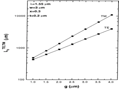
3.13 TE, TM coupling lengths as function of coupler gap for ridge width w of 3^im, aluminium cone. x==0.3, and the lateral clad, t of 0.3p'm. 48 3.14 TE, TM Coupling Lengths as function of coupler gap for ridge width w of 3/«??r, aluminium cone. x=0.3, and the lateral clad, t of 0.2/j,7ti... 48
3.15 TE, TM coupling lengths as function of coupler ga]) for ridge width w of 2.5/J.rn, aluminium cone. x=0.25, and the lateral clad, t of 0.2/xm... 49
3.16 TE, TM coupling lengths as function of coupler gap for ridge width w of 3.5/^m, aluminium cone. x=0.25, and the lateral clad, t of 0.2¡jLm... 49
3.17 TE, TM coupling lengths as function of coupler gap for ridge width w of 3/i?7r, aluminium cone. x=0.25, and the lateral clad, t of Q.2/j,rn. 50 3.18 TE, TM coupling lengths as function of coupler gap for ridge width w of ciluminium cone. x=0.25, and the lateral clad, t of 0.2p?/i. 50 3.19 TE, TM coupling lengths as function of lateral cladding thick, t for ridge width w of 3/um, aluminium cone. x=0.3, and the coupler gap g of 4.5/7777... 51
other is coupling back for our optimum coupler design... 53 3.24 Geometry of the etched ridge... 54 3.25 Single-multi mode regions depending on the guide ridge with tu
and the lateral cladding thickness t ... 55 3.26 Cross section of the devive at the coupling region... 56 3.27 Top view of the coupler with bended sections... 56 3.28 3-D vector BPM simulation for the TE guided mode of the coupler
geometry shown in Figure (3.27) with straight coupling section of 3300 /rnr... 57 3.29 3-D vector BPM simulation for the TE guided mode of the coupler
geometry shown in Figure (3.27) with straight coupling section of 3500 /1777... 58 3.30 3-D vector BPM simulation for the TE guided mode of the coupler
geometry shown in Figure (3.27) with straight coupling section of 3900 iim ... 58 3.31 3-D vector BPM simulation for the TE guided mode of the coupler
geometry shown in Figure (3.27) with straight coupling section of 3700 /im ... 59 3.32 3-D vector BPM simulation for the TM guided mode of the coupler
geometry shown in Figure (3.27) with straight coupling section of
3900 /7777. 59
mode of the straight coupler with a gap of 4.5yu??z and a propagation distance of 4000 ¡.tm... 60 3.34 The applied field and the guided modes; the field of TM mode is
nearly along the applied field, therefore no index change for the TM guided mode... 64 3.35 Top view of the device with counter electrodes. 65 •3.36 Toi5 view of the device with push-pull electrodes. 65 4.1 SEM iDicture of the GaAs/AlGaAs double heterostructure... 67
4.2 PL spectrum of GaAS layers in our wafer. 69
4.3 PL spectrum of AlGaAS layers in our wafer... 70 4.4 Raman spectrum of GaAs and AlGaAs layers... 71 4.5 Etch profiles for different crystall orientations... 76 4.6 Sccinning Electron Microscope (SEM) picture of the etched ridge
with the Wright guide crystall orientation giving the desired etch shape and the lithograiDhic photoresist on it... 76 4.7 SEM picture of the etched guides, side wall smoothness is
important to prevent losses... 78 4.8 SEM picture of the guides with metal electrodes deposited on top
of ridges... 82 4.9 Optic microscope iDicture of the connection with the electrodes on
top of the guides cind the pads... 82 4.10 Optic Microscope picture of the Push-pull type electrodes... 82 4.11 Optic microscope picture of the alignment marks from a processed
sample... 83 4.12 Mask layout; three layer mask with the layer 1 the guide etch mask,
hiyer 2 the electrode metallization, and layer 3 the pad metal mask. The devices are in a 11,920 x 9,750 ¡JLin^ mask area... 84 4.13 Marks for initial rough a lig n m e n t... 85 4.14 Marks for fine cilignment... 85
5.8 Coupling fraction of modes for g=4.25/«m and w - '3μηι... 94
5.9 The parameters of the fabricated active devices... 95
5.10 Parameters of the fabricated active device... 95
5.11 Coupling fraction of modes for g=4:.bμm and w = $μπι... 96
5.12 Coupling fraction of modes for g—4:.25μm and w — 3μητ... 96
5.13 Coupling fraction of modes for g=4.75μm and w = 3μτη... 97
5.14 Coupling fraction of modes lor g—4:.75μm and w — 3μτη... 97
5.15 Least square fit to the Equation (2.47) of the TE data for g = 4.5^i?77, without bias... 98
5.16 Least square fit to the Equation (2.47) of the TE data for g='\ J)μm under a bias V=10... 98
5.17 Least square fit to the Equation (2.47) of the TM data for g = 4.5^?77, without bias... 99
5.18 Least square fit to the Equation (2.47) of the TE data for g=4.25^?77 under a bias V=30... 99
5.19 Least square fit to the Equation (2.47) of the TE data for g = 4.5/i?77, under a bias V=10... 99
5.20 Calculated vcilues of K for TM and biased-unbiased TE as a function of gap... 101
In trod u ction
Integrcited optoelectronic devices made of semiconductors, particukirly semi conductor compounds, have cittracted considerable interest in recent years. Such components may form the basis for integrated optoelectronic circuits in which light sources and detectors, as well as optical waveguide devices and electronic circuitry, are monolithically integrated on the same substrate. Through integration, a more compact, stable, and functional optical system can be expected. Many research groups all over the world are studying to realize this goal.
Optical functional devices that manipulates the light while in transmission are components that have a key position in the present cind future techno logical devices. External optical switches and modulators of multigigahertz
bandwidth and high optical power handling capacity Imve a multitude of applications in the present and future fiber optic systems, not only for telecommunications but for airbone and satellite-based phased cirray radcir and instrumentation, and for optical signal processing applications. Reseiirch on bulk optical switches and modulators began shortly after the invention of the laser several decades ago. The goal of efficient high-speed devices stimulated researchers throughout the world to seek better electro-optic nicitericils and efficient device geometries. With the rapid reduction of loss in glass fibers in the late sixties, research on optical switches and modulators gained new stimulus
are important for future switching networks. The interest in guided-wave optical switches is growing as the signal bit rate in transmission over optical fibers becomes higher, because of their data path transparency.® They are also very important devices for the external modulation of lasers at high data ixite. They cire basically the key devices in an integrated circuit being the intermediate position of manipulating and controlling lightwaves and signals in between sources cind recievers.
A directional coupler consists of a pair of closely spaced, parallel waveguides. The interaction of the evanescent fields of the guided modes in the individual waveguides causes power exchange between the coupled waveguides. The power trcinsfer can be controlled by adjusting the synchronization and the coupling coefficient between the guides. An attractive feature of this coupling effect is its sensitivity to small changes in the values of the structure parameters, relVcictive indices, interguide spacing, guide width, allowing easy control of the energy exchange between the coupled waveguides, by external fiictors such as electric, magnetic, and acoustic fields.®
Up to date several types of directional couplers have been realized with different working principles and on different material systems. Waveguides are the basic tools for couplers, so the material used is important for the purpose. Simply it is the material refractive index difference that is utilized to obtain a waveguide to guide the optical modes. These guides are formed by directly growing different index materials on top of each other in the desired way as well as creciting this index difference through an applied field, as in the case of field induced guides (FfG ’s). Directional couplers using this type of guides were realized.^ Carrier injection type switches,^ gain guide type switches, electrooptic, acousto-optic'
directional couplers,'* vertical directional couplers, FIG type directioiuil couplers, nonlinear directional couplers'* are of a few examples of directional couplers constructed so far.
The material system on which the directional couplers are fabricated is another important parameter. Lithium Kiohate(LiNbOs), InGaAsP/ InP, GaAs/AlGaAs are examples of material types used for waveguides in couplers. Considerable efforts have been made to study LiNhOs optical switches** for such applications as space-division, time-division, and wavelength division photonic switching.® Couplers for lightwave systems made of LiNbOz hcive achieved very high distance times data rate products.® Although LiNbOs ojDtical switches and couplers have attractive features, like low propagation loss and low coupling loss to single-mode optical fibers, they also have drawbacks, such as large device size, cuid the inability to be integrated with other active optical devices, which prevent the LiNbOz switches from being realized into large scale integration.® Therefore, there has been considerable interest in opticcil switches made of III- V semiconductor compounds for those applications, because of their large scale integration capability and their ability to be integrated with other semiconductor devices in order to realize the ultimate goal of Photonic Integrated Circuits (PIC ’s).
This thesis describes work on the polarization splitting GaAs/AlGaAs directional couplers. For successful! utilization of optical intensity modulation devices in commercial systems, such as optical switches and moduhitors which hcive many important apj^lications in broadband communications, optical control of microwave and milimeter wave signals and instrumentation for high speed real time signal processing, several requirements should be met. These are wide electrical bandwidth, low microwave power consumption, hirge optical extinction ratio and dynamic range, low ojDtical insertion loss and polarization independence.Polarization independence is a crucial point for the present cind future applications of guided wave devices.
It has long been recognized that IITV semiconductors offer significcint advantages over other materials such as LiNbO^}^ These include the potential for
end facet preparation (scibe-and-cleave versus cut and polish). The advantages offered by III-V materials, however, have historically been offset by the high insertion loss(> 3 dB) of semiconductor waveguide devices cind the large size (> 1 cm) of conventional integrated optical circuits. Device insertion loss directly reduces the maximum transmission length of communication systems, cind is therefore highly undesirable. A second issue is large device size and incompatibility with the relatively high cost of III-V semiconductor materials.“ Nonetheless, significant progress has occured in the areas of loss and chip size during the past several years. The results of the studies showed that insertion loss cilone, including the problem of fiber coupling, is no longer a serious barrier to the use of III-V semiconductor integrated optics. As a result of improvement in epitaxial growth and waveguide channel fabrication techniques, straight guide propagation loss has also been reduced to levels comparable to that in LiNbO^,^'^ and to the point where overall insertion loss is usually dominated by other factors. Therefore, among all types of optical switches, a GaAs/AlGaAs electrooptic directional coupler is attractive as a cross point element for an integrated switch, because of its low absorbtion loss at long wavelength r e g i o n , f a s t switching speed, low electric power consumption, and wavelength independent operation capability with the advantages of more advanced microfabrication technologies.® In our design of the polarization splitting directional couplers, optical waveguiding is realized using rib waveguides etched into a GaAs/AlGaAs heterostructure, which is unintentionally doped and MBE grown on a [100] oriented semi insulating substrate. Due to depletion originating at the surface and semi insulating substrate interface, it is almost self depleting. Confinement of the guided mode in the guide is ¡performed by utilizing the effective index differences.“
To handle the polarization and polarization sensitivity, we incorporate tunability with the help of rnetal electrodes from Schottky contacts with GaAs/AlGaAs heterostructure, rather than using entirely passive couplers. The bulk electrooptic effect is used to achieve index change with the applied field. The coupler we have designed is basically formed by symmetric waveguides that have bends at both the inputs and the outputs to separate the guides from each other which are coupled in a so called ’’coupling region”. These bends critically effect the device size. To seperate the guides that are coupled with a 7.5 prn centre to centre distance to a point of 30 pm seperation, a distance of 3000 pm is required, because of optimum curvature needed to have minimum loss. Effective index method calculations were used to cinalyse the rib geometry waveguides, to obtciin the guided modes and propcigation constants. The coupling lengths of the guided TE and TM modes were then calculated. The device is designed so that only one mode will be able to propagate through the guides, since the coupler is a single mode operating device. The design of the polarization sensitive couplers using these optical waveguides were carried out using the 3-D Vector beam propagation method (BPM) codes that were developed p rev io u sly .N u m ero u s simulations of the theoretical design were performed to test the structures and to reach the optimum design parameters for low loss and comjDact geometry. Our basic goal was to obtain a geometry that have passively coupling lengths (Lc) for TE and TM modes of which the L d T M ) is twice as much as the Lc{TE). This results in splitting of TE and TM polarizations at the outj^ut jDorts. The electrooptic efhect is used to change and tune the coupling lengths by an applied DC bias to the Schottky electrodes over the guides in the coupling region. The applied electric field induces a change in the refractive indices under the rib geometries which effect the coupling lengths of the TE and TM modes differently. This allows the possibility to route TE polarization to the desired output port. So this enables us to achieve easy contx’ol of the coupling of the modes with the applied field, resulting a coupler that can be placed a through state for TE or for TM polarized guided modes.
coiq^led mode theory cuid the Bea.rn Propagation méthodes, the effective index method, and an introduction to the basic theory of operation for directional couplers.
I l l chapter 3, we present our work on the design of the Polarization
Sensitive Directional Couplers. The geometries used and the effective index method calculations used to obtain a single mode, low loss compact geometry , calculcitions of the coupling lengths for the TE & TM polarizations and, results of the Beam propagation Method (BPM) simulations are presented. Finally, a brief description of the mask design and the mask features are given.
Chapter 4 contains a detailed description of the fabrication of the devices, with standard processing equipment and techniques, optimization of process pai’cimeters especially for obtaining guides of milimeters long and a few microns of thickness. We begin with characterization of the starting wafer grown for this purpose with SEM, and optical spectroscopy and explain the processes to fabricate the device.
ChaiDter 5 describes the characterization and testing of the Polarization Sensitive Directional Couplers, with a brief description of the test setup, and the results.
T h eoretical Background
The fundernantal idea behind the integrated optics is to handle light with waveguides, cind not by free space optics. Nearly in all opticcil devices, opticcd held is guided by dielectric waveguide structures, i.e, by properly shaped dielectric prohles. Although, rnetal clad structures represent an alternative way for Wcive- guiding that is popular for microwaves, they are rarely used in integrcited optics ci.s the metals are too lossy in the optical wavelength region. The main results of the waveguide theory are the number of guided modes for a given dielectric profile, the effective index and the optical field for each mode. A siricdl number of devices call for the analysis of the radiation field and, in particular for leaky modes, i.e, for resonances in the radiation field. These result, in turn, form the basis of device modeling, e.g, of the coupled mode theories describing directional couplers.
Waveguide analysis requires the solutions of partial differential equations, i.e a recisonable cimount of computer power. As a consequence, a lot of work in the pioneering days of integrated optics was focused on approximations such as the effective index method (EIM) or Marcatili’s m e t h o d . W i t h the increasing power of computers, increiisingiy numerical solutions such as finite element (FE),^^ finite difference (FD)^^ and method of lines (MoL)^^ cilgorithrns cire used to analyze waveguide structures. Nevertheless, approximate methods in general and the effective index method in particular represent the work horses for design and
choice of process and the required aspect ratio i.e. Etching depth / structure size determines the shape of the waveguide, its roughness, and importantly the fabrication tolerances, especially the waveguide width. For the III-V semiconductor material systems, the layers of different materials for these waveguides are grown by epitaxy, usually by metal organic vapor phase epitaxy (MOVPE), or metal organic molecular beam epitaxy (MOMBE), or sometimes by liquid phase epitaxy (LPE). In contrast, for the silica-on-silicon matericil system
(SiO-i/Si), the layers are fabricated by deposition - various types of chemical
vapor deposition (CVD), or flame hydrolysis, or by thermal o x i d a t i o n . T h e choice of the fabrication process defines the ranges of available layer thickness and material compositions. In addition, it determines the roughness of the interfaces cuid the fabrication tolerances of the material composition and the layer thickness.
2.1
R a y O p tics A n d G u ided M od es
n.
n
f
Figure 2.1: Incoming ray at an angle
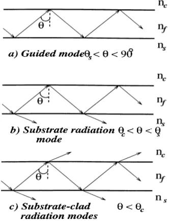
Consider an incident coherent light at angle 6 between the wave normal cind normal to the interface in the step index slab waveguide, as shown in Figure (2.1). The simplest optical waveguide is the step-index planar slab wciveguide. The critical angles at both upper and lower interfaces, respectively, are.
Oc = shi '(n c/n f) O s - s i n ^ { n s l r i f ) (2.1)
In genei’cil, > rp, and Os > 0^. On the basis of these two criticid angles, three possible ranges of the incident angles Oi exist: (1) Os < 0i < 90°, (2)
Oc < O2 < Os^ (3) ^3 < Oc- Three different zig-zag I'ciy optical pictures, which
differ depending on the incident angle, are shown in Figure (2.2).
a ) G u id e d m o d eB < 0 <
96
b ) S u b s tr a te r a d ia tio n 0 < 0 < 0 m o d e c) S u b s tr a te - c la d r a d ia tio n m o d e s 0 < 0..Figure 2.2: Zig-zag wave pictures of ’’modes” propagating along an o waveguide
tical
When (1) occurs, the light is confined in the guiding layer by total internal reflections at both upper cind lower interfaces and propagates cdong the zig-zcig path. If the waveguide material is lossless, the light can j^ropagate without attenuation. This case corresponds to a guided mode, which phiys an important role in integrated optics. On the other hand, when (2) occurs, the light is totally reflected at the upper interface while it escapes from the guiding layer through the
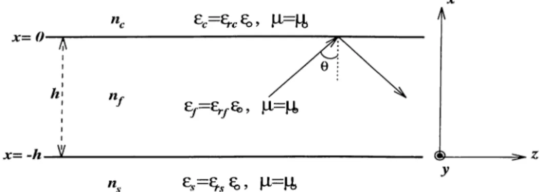
at the interlaces and the accompanied phase shifts.^'* The cinalytical results cire consistent with the derived results based on wave optics, in wave optics, modes are generally characterized by propagation constants, while they are classified by tlieir incident angle 0 in riiy optics. The plane wa.ve propagation constant in the wave normal-direction is defined as AiqU/, as shown in Figure (2.3), where
ko — 27t/A and A is the light wavelength in free space. The relationship between the incident angle 0 and the propagation constants along the x and directions then becomes:
Figure 2.3: Wave-vector diagram
kx = konfcos0 kz = koiif sinO = /3. (2.2) We let, kz — [3 for lossless waveguides in which ¡3 is equivalent to the plane wave propagation constant in an infinite medium with an index of n j sintl. Therefore, effective index, N , of a mode can be defined as: (3 = koN or N = rifshiO. Actually, the guided mode proj^agating along the 2; direction effectively sees the index N. It should be remembered that the guided modes can be supported in the range of 0,, < 0 < 90°. The corresponding range of N is 77,,, < N < rij.
Sirnilcirly, the radiation modes exist in the range of N < iig.
2.2
W ave E q u ation s For a Slab W aveguid e
Maxwell’s equations in isotropic, lossless dielectric medium are,
V 7 f '
V x £ =
V x / / - e o n ^ ^ (2.3)
where cq and go are the dielectric permittivity and magnetic permeability of
free space, respectively, and n is the refractive index.
; guiding is in layer f. Assume non-magnetic materials for integrated optics applications.
Figure 2.4: A slab waveguide The wave equation for a field in the sccilar form is;
+ klnf-if) = 0 (2.4)
Suppose that the plane Wcive propagates along the ^-direction in the orthogonal coordinates { x ,y ,z) with the jDropagation constant /3 (we assume that the field propagates with the same ¡3 in the ’r-direction as a result of phase matching condition; kzi = k^,2 = k^^ = ¡3 = koUeff). The electromagnetic fields vary as;
equations for the T E and 'TM modes are; diE, dx^ dHly dx'^ ■ + {kf ^nf - I}'‘)E, = 0 II - tr _ 1 (2.6) WjlQ Z - iwfio dx· r\ + {ko^Ui^ -- = 0 E - _ i dH , (2.7) ilOtoU'^ dx TE TM. (Ey’fi
F ig u re 2.5: Modes in a slab waveguide
The field solutions and the boundary conditions at the interfaces x — —li and a; = 0 lead to the eigenvalue equations that determine the propiigation characteristics of the T E and T M modes. The two orthogonal T E and T M modes must be distinguished to discuss disj^ersion characteristics of the guided modes. Then, the fields for T E mode in the regions I, II, III become;
Ey = EcC^ fo r a; > 0 (in the cladding)
Ey — fo r — h < x < 0 (in the guiding layer)
_ £J^^[ois{x+li)]^{-ikzz) fo r X < —h
and from equation(.) we have;
k J + /3^ = k o W
(in the substrate)
(2.8)
Applying the boundary conditions at the interfaces at a; = 0 and x = and the fact that tangential components of the fields E and H are continuous;
i?,X0+) = AV(O-), Ey{h-) = Ey{h^) and / A ( / r ) = /f,(h+) (2.10) fo r x > 0 (2.11) hL = IXUB-Q ■ ( /7^ - fo r h < X < 0 f o r x < - h
and eliminating the unknowns from the equations, we obtain an eigenvalue equation; cy^ -4- rv„ (2.12) I 1 “h Cis tanA:^/i 7—7 -t ( i - 1 ? )
The same ¿inalysis ¿ipplies to the T M mode and an eigenvalue equation for T M is obtained;
T) ^2CVc
i a n k j i = — ---- VicJ^ — (2.13)
■ ns2 kx /V Uc^ kx /
If the structure is symmetric then ric = Ug and ac — cxs = a. There are two choices for the description of the field in the guiding layer, depending on whether a symmetric (cosine) or antisymmetric (sine) mode is excited. The fact that the modes can be uniquely characterized in terms of even or odd groups is a natural consequence of the even symmetry of the index structure. The sign of the field in the lower substrate is positive for the even modes, and negative for the odd modes. The characteristic eigenvalue equation for the T E modes in a symmetric waveguide is:
,kJi^ \ f - for even(cos) modes t a n ( - ^ ) = < ^ \ ^
2 for odd (sin) modes The characteristic equation for the T M modes is;
,k^h. I { ^ ) f- for even(cos) modes m odes If we rearrange the eigenVcilue equation for the symmetric T E mode;
ah T kg^ h kg^ hi —— tan —— (2.14) (2.15) (2.16)
and defining x = ( ^ ) and y = ( ^ ) , we obtain the following curves as solutions lor the eigenvalue equations. Number of guided modes in the structure will depi'iid on the iDarameter where ~
Figure 2.6: Parametric solutions of the eigenvalue equation
The guided modes are in the range kgUg < /d — koUeff < kouj. The following definitions can be used to obtain a normalized eigenvalue equation;
■n 2 ... 2
Ux — Kc. nj^ - U s “
where the asymmetry parameter is in the range;
(Asymmetry Pariimeter) (2.19)
a — 0 lor symmetric slab geometry
0 < a < oo for asymmetric slab geometry (2.20) When the waveguide parameters are given, the eigenvalue equation can be solved numerically to evaluate the dispersion characteristics of the guided modes. Such a numerical evaluation is applicable to any step-index 2 — D waveguide
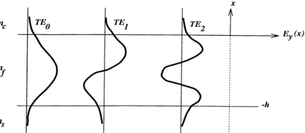
l î y ( x )
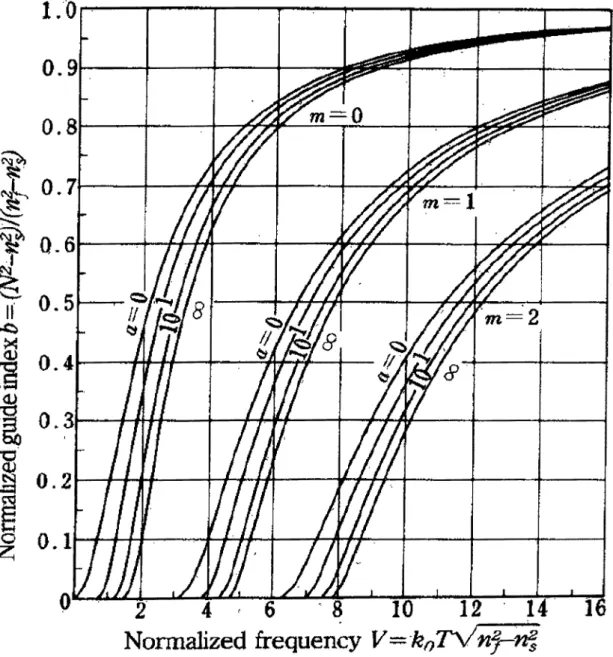
Figure 2.7: Optical electric field clistrubutions of TE guided modes. by introducing the following normalizations: Normalized frequency (normalized thickness) V and the normalized guide index b are defined cis;
V — koh^Jn/^ — Us'^ (2.21)
n - n ^
b = ^ (normalized index, 0 < 6 < 1)
— n / (2.22)
Using the above definitions the eigenvalue equation(2.12) C cin be written cis;
V V i — b = tan ---^+ tan ^y ----^(normalized eigenvalue equation tor T E )
(2.23) Based on the preceeding equation, the normalized dispersion curve (that is, the relation between b and U) is solved numerically, as shown in fig(2.8) where the b is obtained in terms of V and as a function of parameters m and a. When the waveguide parameters, such as the material indexes and the guide thickness.
are given, the effective index of the guided mode is obtained graphically. The waveguide parameters ¿ire usually determined on the basis of cut off of the guided modes. When the incident angle 0 becomes the critical angle Og, the light is no longer confined in the guiding layer, and it begins to leak in to the substrate at the interface x = —h. This situation is called cut off of the guided modes, in which the effective index n^ff = ns(b = 0). From the normalized equation, the Vcdue of V at the cut off is given by;
V = tan ^ ^/cı + rmr = f/f, + rmr (2.24)
Vo is the cut off value for the fundemantal mode. If the normalized frequency V
of the waveguide ranges over Vm < V < Idn+i, the T Eq, TE i - ■ ■ and the Ti?,« modes are supported; the number of the guided modes is + 1. For symmetrical waveguides [ug = iic), Vo = 0. This implies that the fundemantal mode is not cut off in a symmetrical waveguide.
For the T M modes, the analysis is similar to the preceeding. Since Hy cind Eg: are continuous at the interfaces, however, a square of the index ratio is additionally included in the eigenvalue equation;
v V T (2.25)
c ]j 1 — b ' c — a \ 1 — b
The above is the normalized eigenvalue equation for T M modes where c is defined as c = —
2.3
E ffective In d ex M eth o d
Mode structure analysis of semiconducting waveguides are difficult and require detailed calculations. In this section, a method known as the effective index method is introduced briefly. However, there are cipproximate methods that usually give quite accurate results for design purposes. This method gives universal dispersion curves of the normalized parameters (6, F, a) for slab Wciveguides.
Figure 2.9; 3-D waveguide with a step-index profile
Figure (2.9) shows an analytical model where a step-index rectangular Wcivcgiiide is surrounded by different dielectric materials. Under the well-guided mode condition, most of the optical power is confined in region I, while a smcill amount of power travels into Regions II, III, IV, and V, where the electromagnetic fields decay exponentially. Even less ¡Dower should penetrate the lour slmded areas. Only a very small error, therefore, should be included in calculating the fields of the guided mode in Region I provided the field matching at the four corners of the shaded areas is not taken into account.
The effective index method converts a two-dimensional problem into two, one dimensional problems. Consider the buried step-index rectangular waveguide shown in Figure (2.10a).
X JS) n„ n. w. ■ ^ y (a) n„ n„ (b) Figure 2.10: n e f f (c) n .
To use the effective index method, we first stretch the waveguide out along its thin cixis (in this case cdong the y-axis) forming a i^lancir shib waveguide. Figure (1.9b). The thin one-dimensional slab waveguide can now be cinalyzed in terms
of T E and T M modes to find the allowed value of fd for the wavelength <ind mode of interest. Once /3 is found, the effective index of the slab is determined through the expression nefj = where A:o is the vacuum wave vector of light being guided. After this effective index is determined, we return to the original structure and now stretch it along the thick axis, in this case along the x cixis, forming a slab waveguide in the x-direction. Figure (1.9c). The modes for this Wciveguide can now be found in a similar fashion, only instead of using the original value of the index for the guiding him, the effective index found in the first step must be used. The value of ¡3 to be found from this last step is the true value tor the mode.
As with the wave analysis, one must be careful to use the proper characteristic equations tor each waveguide. For examj^le, if in the figure above, the electric field is polarized in the .x-direction, then for the thin waveguide the field will act cis a T M mode, and the cippropriate characteristic equation must be used. When the thick slab is analyzed, this same held will look like a T E mode, and so the characteristic T E equations should be used to find ¡3. When the index difference between the guiding and the cladding hiyers is large, using the proper characteristic equations is critical for getting a reasonable answer.
The slab waveguide is a two dimensional structure, providing no confinement of the wave in the ^-direction in Figure (2.4). A slab like structure known as the rib xoaveguide is often used in optical integrated circuits to conduct light from point to point on a substrate. The rib waveguide geometry is shown schematically in Figure (2.11).
• The aspect ratio, ^ (in the figure) must be small,
• The effective indices for regions I, II, and III must be very close to each other.
These two conditions seem stringent but are very nearly met for a wide variety of waveguide structures used in integrated optical circuits.
2.4
S in gle-M od e
3 — DW aveguides
In multi-mode waveguides supporting more than two guided modes, mode interference and undesired mode conversion due to small disturbances reduce waveguide device performance significantly. To avoid this, most waveguide devices consist of single-mode 3 — D waveguides supporting only the fundernantcil mode. In slab waveguides that we are interested, possible range of the normalized frequency is determined by V — so that the fundemantal mode with the mode number m — 0 is guided while the first order mode with rn = I is cut off. Using equation (2.24), the range of V,
tan ^-y/a -f 7T > U > tan ^^/a (2.26) to meet the single mode propagation requirement can be found easily. The measure of assymrnetry a is zero for symmetrical waveguides, then this gives us the relation or the range for V to have a single mode in symmetrical guides as;
2.5
C ou p led M od e T h eory A n d C oupled
W aveguid es
In many optical integrated circuits, guided modes propagate with coupling. Coupling of optical power from one guide to an other one can be analyzed by coupled mode theory. Various guided modes exist in a lossless Wciveguide which is uniform along the propagation direction. These are normal modes (eigenfuctions in boundary value problems) defined by the waveguide structure cind its boundary conditions. An orthogonal relationship holds among the modes. Thus, each mode propagates without mutual coupling and carries power independently.
There are two methods for analyzing optical wave propagation in perturbed (coupling is a perturbation effect) waveguide systems;
1. Compute the normal modes of the waveguide using Maxwell’s equations. 2. Express the perturbed wave behavior by summation of normcil modes in
the unperturbed waveguide system.
Method 1 should give a good solution, but the problems can not generally be solved easily. On the contrary, method 2 gives only approximate solutions but is straightforward and simple. This method also allows for a qualitative understanding of essential phenomena, and approximate solution is surprisingly good. Thus, coupled mode theory is a method that can be used to describe the wave behavior in a ¡Derturbed waveguide system by means of the known normal modes of the unperturbed system. Applications of this theory are very broad.
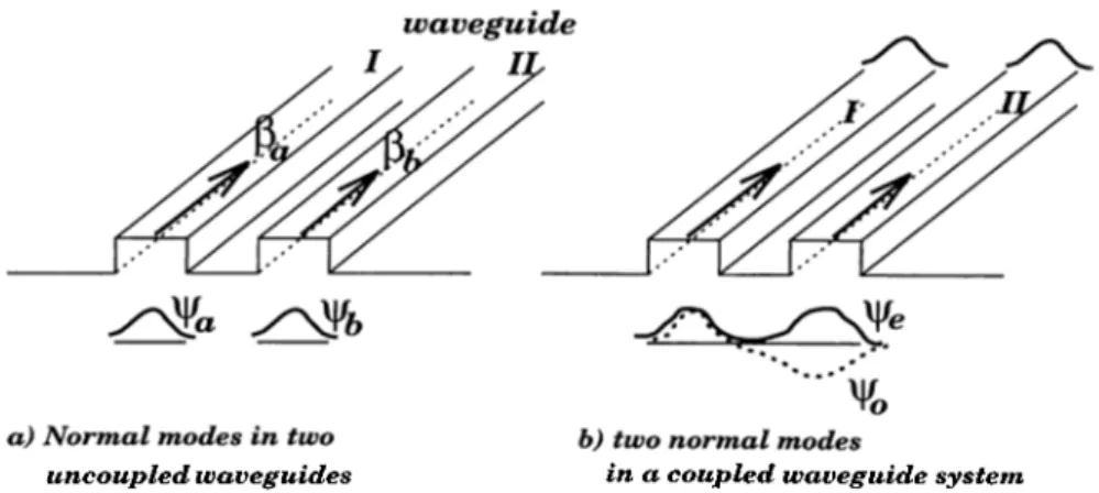
Consider the fundemantal phenomenon of two modes with coupling present. Next, consider two waveguides I and II, as shown in fig.(2.12). When they are separate enough from each other, two normal modes, a and 6, propagate independently on each waveguide with fields ipa and and with propagation constants and ¡3^ {fia < /3b), respectively. When the waveguides are uniformly coupled (perturbed) by reducing the sei^aration, the original normal modes ?/>„ and ipb no longer exist, and two new normal modes and i/)o propagate along a coupled waveguide system consisting of waveguides I and II, as shown in Fig
u n c o u p l e d w a v e g u id e s in a c o u p l e d w a v e g u id e s y s te m
Figure 2.12; Norrricxl modes in waveguides in the absence and i^resence of coupling.
(2.12b). ( ?/>e and V'o correspond to a symmetric mode and an cisymmetric mode, respectively.) Propagation constants of these two modes are /3^ (larger than
f3b) and f)o (smaller than (ia)· ''/’e and ij^o can be excited independently by an
appropriate method. Depending on the excitation condition, the two modes cire excited at the same time cind yield a beat, as shown in Fig (2.1-3), since the propagation constants are not very different from each other. When looking at wave behavior along waveguides I and II, wave power appears to transfer back and forth periodically between I and II (that is between ?/>„ and ?/>(,). The coupling effect is stronger when ¡3a and j3b are approximately equal.
The preceding is the fundemantal concept of coupled mode iDi'opagation cilong the coupled waveguides. The purpose of the coupled mode theory is to obtain
Figure 2.13: Two normal modes in a coupled wa.veguide system and power trcvnsferring.
?/>e, i/j„, beat period, and other quantities using V>o. and ^¡, from coupling features. Opticcxl waves ?/)„ and propagating along the coupled waveguides I and II are expressed as;
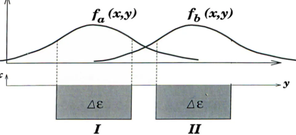
y, z, t) = A(z)e (2.28)
y, z, t) = B(z)e~'^'’"fb{x, (2.29) where fa. and /¡, are field distrubution functions that are normalized by power How over a cross section. If coupling between I and II is reduced to zero, and 'ihh are reduced to two independent original modes, and A(z) and B(z) are reduced to constants. In this case, coupling is present, and therefore, A(z) and
B{z) are no longer independent. The coupled mode equations include functions
of only 5;, as follows;
= - i K a h for {¡3a <> 0)
(2.30) = -г7f6αA(^)e+d/^<--/5α)- for < > 0)
where Kab and Kia are coupling coefficients between two modes. The term e^hPb-Pa)z right-hand-side corresponds to the phase-constcuit (mismatching) of the modes. When Kab — Kba = 0 in above equations, then ipa cind ipb are reduced to two original waves.( The above equations are derived from Maxwell’s equations.) The coupling coefficient is a measure of spatial overlapping
2.6
C ou p lin g L en gth A nd P ow er Transfer
Behavior of coupled waves can be determined by obtaining propagation constants of the waveguide system from the coupled mode equation. Two cases of propagation of two waves exist, codirectional and contradirectional. However, due to the fact that in our device we will utilize the codirectional propagation, we only consider this case {[da > 0,^t > 0). The coupled mode equations are then reduced to;
dA[z) dz dB{z) dz (2.32) (2.33) where Kab = Kla — i^· positive vcilue) is set for simplicity. By introducing a new quantity 2A = fh — fda for convenience, and assuming the solutions for A{z) and B{z) to be in the form;
A{z) = (2.34)
B{z) = (2.35)
a quadratic equation for 7 is then obtained whose roots are; 7 = db\/A^2 +
Then the solutions are written as follows;
A{z) = — ¿Az
(2.36)
B (z) KA,, K A . I +/'Az
(2.38) VA^2 + A 2 + a '
Then by using the above equations, the following can be derived;
?/, .^) = [/lee~'^'=^ + (2..39)
y, ^) = i/)e'“^' (2.40)
where the ratio of Ag and Bg is a j^ositive constant, and the ratio Ag and Bg is a negative constant. The following relations are also defined;
f^e — Pm + Pc Po = P m - Pc where; Pm = {Pa + Pb) /3g = C IO + A 2 (2.41) (2.42) (2.43) u v a v c ^ u i c l c s II (a) o P« j __ Pft 2 ^ -P. P c P« (b) P. ZJncoujylcd coujplcd
Figure 2.15; Propagation constants in the case of codirectional coupling. Equations (2.39,40) indicate that optical waves ^a. and i/’fc propagating along waveguides I and II are expressed by a linear combination of two waves with the propagation constants Pe and Pg. Pg and /?o, therefore, ¿ire the
B{z) =
He (2.45)
since fa and /j are expressed by means of a normalized power flow, the power flow along waveguides I and II cire given by |yl(2)|^ and \ B ( z ) f respectively. Thus, the preceding equations can be written in a power form as follows;
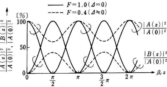
|A(o)r \B{z l^(o )r = 1 — Tsin'^ Pc = Fsin^ PeZ (2.46) (2.47) where F — Pc 1 Some calculated curves of Equations (2.46,47) are
+ ( A ) - V > y
illustrated in Fig (2.16).
C % )
--- F = 1 . 0 ( J = 0 )
--- F = 0.4(2l^0)
The power of waves propagating along the two guides vary or beat periodically.
F means the maximum transfer of optical j^ower from the guide I to 11. The
maximum i^ower transfer occurs at distance L, given as;
L = —
^ 2fC (2.48)
This Lc is called the coupling length. When the two modes are synchronized, tlnit is when fia = fdh·, F = 1 holds, and the coupling length is reduced to Lc — From this derivation, the following two important features are revealed; •
• When the two modes are synchronized, the coupling coefficient K influences only the coupling length, and a 100-percent power transfer is obtciined, regardless of K.
• When the two modes are not synchronized, a 100-percent power transfer can not be obtained cind is determined by the coupling coefficient and the degree of synchronization.
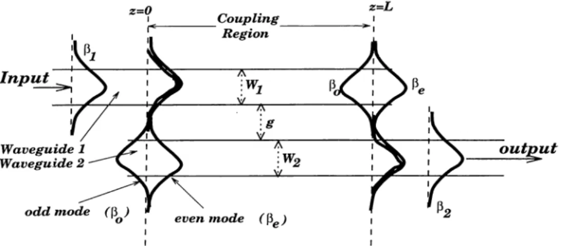
the maximum and the minimum output levels) is possible. Consider a typical directional waveguide corp^ler, as the one shown in Fig(2.17), where fdy and ^2 are the propagation constants of the uncoupled waveguides and ¡3^. and f3o are the propagation constants of the even and odd modes of the coupled waveguide system derived from the coupled mode theory. The guided mode incident from waveguide 1 excites the even and odd modes in phase with the same cunplitude at z = 0. The phcise shift between the even and odd modes become tt when the
propagation distance L is;
Hence, at the output end of the coupling region, z = L, the resultant electric field distribution of the even and odd modes coincides with the electric field distribution of the guided mode in waveguide 2. In other words, all optical |)ower is fed into waveguide 2. L is defined as the coupling length, where 100-pcrcent
W a v e g u i d e s p a c i n g g j(L m )
a)W^W^4\T nt
W a v e g u i d e s p a c i n g g m )
h)W^4\im, =3|i m
F ig u re 2.18: Variations of propagation constants of nornicil modes and the coupling coefficient with the waveguide spacing g. (a) Symmetrical (b) Asymmetrical directional couplers.
power is transferred if the two waveguides are identical. The power transfer mechcinism is thus well understood by interference between the normal even and odd modes in the coupling region.
The projDagation constants ¡3e and ¡do are shown in Fig(2.18) against the waveguide spacing g lor a directional coupler. In a symmetrical directional coupler where W\ = W2 = if-mi and fdi — /32, considerable coupling occurs in
the g < 8pm range. On the other hand, in a symmetrical directional coupler where wi = 4pm, W2 = ‘Spm and, hence, /3i > /?2, the coupling is not noticeable
unless g is less than bpm. The power transfer due to the mode coui^ling is generally chciracterized by a phase mismatch {[3i — ^2) between the wiiveguides
and the coupling coefficient K. Earlier the coupling coefficient was defined as;
K = - A ) (2.50)
Therefore, K is easily evaluated by calculating the propcigation constants of the normal modes, on the basis of effective index method. Once K is specified, the directional waveguide coupler is analyzed based on the coupled mode
different approaches have been d e v e lo p e d .T h e so called beam propagation method (BPM) has been successfully used to analyze a wide spectrum of guided- wave .structures. BPM is bcisically formed by approximate mathematiccil methods for solving problems of light propagation in dielectric optical waveguides of arbitrary shape. The method is only restricted by the conditions that reflected waves can be neglected and that all refractive index differences are small. W ith these restrictions, the waves described by the BPM can be regarded as cipproxiiTicite solutions for the scalar wave equation;
y·, z)k'^ij) = 0 (2.51)
where ?/> describes an optical wave characterized by the free-spiice propagation constant k = ^ moving in a medium with the refractive index distribution
n [ x ,y ,z ). Also, even where analytical techniques are cvvailable, numerical techniques are often times employed to verify the designs before proceeding to invest serious effort in making new structures.
The most rigorous way of handling electromagnetic wave propagation in integrated optics is to solve the Maxwell’s equations with appropriate boundary conditions. However, PIC structures hcive certain features which makes this approach very difficult to implement. The main reason is the large aspect ratio between the propagation distance and the transverse or hiteral dimensions of the propagating energy. The cross section may be contained in a few microns by a few microns wide window, but the propagation distance could be centimeters long. Therefore, to establish a fine enough grid for a boundary-value approach would pose a great challenge for computer memory and CPU performance.
Fortunately, the guided waves in PIC ’s have certain other properties which allow some approximations to be made. For example, in most cases the scalar wave equation is sufficient to describe the wave propagation. Secondly, the phase trouts of guided waves are nearly planar or their plane wave spectra are quite narrow. Therefore, they are paraxial. Thirdly, index changes along the propagation direction tend to be small and gradual in many situations. Hence, the wave amplitudes change slowly and back reflections are negligible in these Ccises. Under these conditions it is possible to reduce the scalar wave equation to the paraxial wave equation, which Ccin be written as;
d f _ d - ‘f d-‘i, ZlkQl'lp „ Q 9 O 9
oz ox^ oy^ + ko^[n'^(x,ij, z) — (2.52)
where ?г,. is a refractive index that describes the average phase velocity of the wave, and = E{z)U(x,y). That is, n,. determines the rcipidly varying
component of the wave, and ?/> includes the slowly varying amplitude along the propagation direction. Thus for the polarization of interest, e(xpy,z) =
?/, The index ?2,. must be chosen as the index of the substrate. The paraxial wave equation describes an initial value problem as opposed to a boundary value problem. As a result, one can start with an arbitrary initial wave amplitude, tf)(x,y,0), which could be a Gaussian beam formed by a lens, for example. The resulting amplitude A z away can be found by integrating the paraxial wave equation over A z. Repeating this procedure, one can find the evolution of the initial held profile over the waveguide. Note that one only needs the field at z = 0 in order to calculate the field values at z = A z. Therefore, there is no need to store or manipulate the field values at every grid point in the ^-direction as required in the solution of the boundary-value problems, thus it does not have cpu problems. Furthermore, all parts of the wave, including the guided and the radiation spectrum, are hcindled together.
The initial procedure for BPM involved operator techniques and F F T ’s. Recently, however it has been shown that algorithms which are much more efficient cind robust can be generated by using finite-difference techniques.^'
mentioned in the preceding chapter briefly, the coupler is basically a device of coupled waveguides. In directional couplers, two waveguides are brought in close proximity to each other and coupling of the guided modes propagating ¿dong the guides takes place. The directional coupler we designed hcive two symmetric strip-loaded rib waveguides and the coupling is codirectional.
In our design, we used unintentionally doped bulk GaAs/AlGaAs heterostruc tures grown on serni-insulating GaAs substrates by MBE. The wave-guiding tcikes place in the higher index GaAs core region and the confinement of the guided mode is done by the index difference of MBE grown layers in the vertical direction. The effective index difference caused by the rib geometry brings the confinement of the mode in the latercil direction under the rib. The use of the GaAs/ AlGaAs material system was explained previously and is rnairdy due to the ultimate gocd of integration with other optoelectronic devices. The aluminium fraction
X of the double heterostructure composition will determine the index difference
between the layers and so is an important ¡parameter of design; the propagation of the guided modes and the guiding will be effected by that parameter. Thus, the aluminium composition is a tuning pai’cirneter in our Ccdculations. Another important point is the single-mode operation of the device. Coupling mostly
takes place in the straight section (coupling region) of the coupler in which the two guides are separated by a distance of only a few wavelengths of the light propagating through the guides. At the input and the output ports of the device, however, the waveguides should be separated by a distance large enough to have easy and efficient coupling to the fibers. We, therefore, used curved waveguides attached to the straight section of the guides both at the input and the output ports which separate the coupled waveguides. This, of course is an importcuit parameter that effects the device size. In fact all these parameters, the guide width the guide separation g (gap between the guides) in the coupling region, the bend radius R of the curved waveguides, the aluminium concentra.tion x of the material system are the parameters that we have dealt with to obtain a design yielding a single-mode, low-loss and compact device geometry leading to a Polarization Splitting Directional Coupler. The operation wavelength was chosen as A = i.hprn which is in the range for fiber optic telecommunications (A = 1.3 — f.6//?7r).
3.1
G eneral O verview o f S tru ctu re
in figure (3.1) our MBE grown double heterostructure used to fabricate the directional coupler is shown. The guided mode propagates in the core GaAs region. The core GaAs (higher index region) is stacked between two lower index
n=l Air n Al^Ga^ AsX l~x Al Ga^ AsX l-x 1 . 1 ^GaAs GaAs A1 1 Y n
AlGa^ AsX I’X Al Ga^ AsX l,x
A1 1 \'/
”^GoAs SI GaAs substrate
tc
AlxGui^xAs Iciyers and the entire structure is grown on an semi-insulating GaAs
substrate. The thickness of the bottom cladding layer, djc, has to be large enough to prevent the guided mode to penetrate into the SI GaAs substrate region so as not to have losses in the substrate due to the overlapping of the substrate and the guided mode. The index difference between the vertically stacked layers is enough to confine a guided mode in the vertical direction (sirnihir to a slab waveguide). For lateral confinement of the guided mode, we have to etch a rib on the upper or top Al^Gai-^As cladding layer and obtain an effective index difference under the rib to confine the mode laterally.
In figure (3.2) we show a rib etched on the top cladding of the double heterostructure geometry. The rib height (or etch depth), h, the rib width, to, are important parameters that define guiding and will be important parameters in obtaining single-mode geometry. Becciuse the guides cire expected to be long, lithogra23hy and alignment requirements impose some limitations on the rib width, w. Below 2pm, it is extremely difficult to align the mask and the sample for millimeter long structures. Furthermore, because we will use meted electrodes on the top of the guides, top of the ridge should be wide enough for at lecist 2pm wide electrodes. Considering that the chemical wet etching of the rib will result in an undercut, we Imve decided to use a 3pm wide stripes on the mask to define the waveguides. For our etch depth, this results in a rib geometry as shown in figure (3.3).
- 5 - 2(hltcin55) \x,m \ 0 ! = 5 5 A \h JL-u c i
---Figure 3.3: Expected rib geometry after wet etch
Several considerations determine the optimum layer thicknesses in the heterostructures to be used for the directional coupler. The upper limit is determined by restrictions on the growth time and cost as well as the necessit}'^ of self depletion for low microwave and optical losses. The lower limit is set by the need tor an effective index contrast and the need to avoid the overlap of the guided field with the metal electrode, again to prevent losses.
3.2
T h e C oupler G eom etry
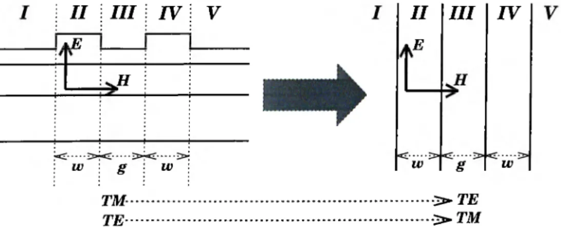
We begin the design of the coupler geometry by calculating the propagation constcints of the guided modes in the coupler geometry. The coupler we are designing, as presented in the preceeding section, is formed from lour layers of materials in vertical direction. The figure below shows the cross sectional schematic of the coupler (two coupled waveguides) in the coupling region ;
g — ---1
II III IV s u b s t r a t e
Figure 3.4: Cross sectional view of the coupler in the coupling region We utilize the effective index method to simplify the above structure. As seen in figure (3.4), we have five different regions where the regions 1, HI, V and