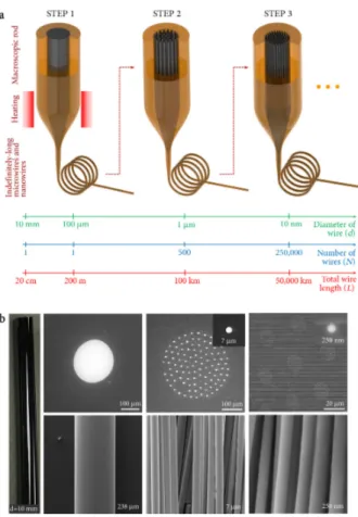
Figure 1. (a) Schematic of the iterative size reduction methods to produce ordered, indefinitely long one-dimensional chalcogenide nanowire arrays. (b) Using multiple thermal drawing technique, a 10 mm chalcogenide glass rod (Se) is reduced to 250-50 µm single wire (reduction factor 40-200x). For the second step, ~100 selenium wires are cut and tighly packed and redrawn to 7 µm (reduction factor 34×) to obtain hundreds of meters long ordered selenium microwires. In the final step, previously obtained selenium microwire arrays are cut, packed and redrawn to 250 nm hierarchically ordered nanowire arrays (reduction factor 28×, total reduction factor is 40,000×). Nanowire arrays are obtained as embedded in a dielectric polyether imide encapsulation. Wire array cross sections with well-ordered wires and extracted, globally oriented slivers are shown after each step.
Macroscopic Photoconductive Nanowire Arrays
Mehmet Bayindir1,2,3*, Mecit Yaman1, Erol Ozgur1,2, Ozan Aktas1,3, Tural Khudiyev1,2, Mehmet Kanik1,2, HakanDeniz1
1UNAM-National Nanotechnology Research Center, 2Institute of Materials Science and Nanotechnology, 3Department of Physics, Bilkent University, Ankara 06800, Turkey
Abstract—A novel high-throughput fabrication technique to
produce polymer embedded functional chalcogenide nanowire arrays is demonstrated. Indefinitely-long selenium nanowire arrays are obtained and their size dependent conductivity is investigated. Logarithmic increase in photo-conductance is observed.
Keywords; top-to-bottom nanofabrication, chalcogenide nanowires, photoconductance
I. INTRODUCTION
One dimensional nanostructures are expected to stay at the forefront of nanotechnology and materials research for a long time. Their promise as high performance functional elements in electronics, photonics and other sensing/ actuation applications is supported by a myriad of synthesis, ordering and manipulation techniques. The current state of the art in nanowire fabrication is impressive in its variety and depth [1]. However inexpensive fabrication of ordered nanowires arrays at high production rates, with simultaneous control of diameter, length, position and orientation still does not exist [2]. Both theoretical and experimental nanowire research, and technological applications can benefit from fresh approaches from novel nanowire fabrication schemes.
One such perspective could be the fabrication of nanowires that truly bridge the nano and macro worlds addressing high-throughput, accessibility and simplicity. We reported a simple top-to-bottom production method to obtain meters long, ordered, semiconducting and polymer nanowires and nanotubes with uniform diameter, homogenous distribution, and endlessly parallel orientation [3]. A novel iterative thermal size reduction technique is used to stepwise reduce a macroscopic rod material down to ordered arrays of extremely long nanowires embedded in a polymer matrix (Fig. 1). In this way, we produced for the first time, millions of ordered, indefinitely long, polymer embedded chalcogenide nanowires, and core-shell arrays. Obtained wire diameter's range is as wide as 10 nm to 100 μm, and are highly uniform (standard deviation within 5% of wire diameter). A wide range of materials such as chalcogenide glasses, a phase change chalcogen and piezoelectric polymer PVDF are obtained as nanowires, and also nanotubes. Resulting nanowires / nanotubes can be used either as free standing slivers, after chemical extraction from the jacket fibre, or used as embedded in the polymer fiber. In the latter case, encapsulating flexible fibre facilitates electrical contact and handling, and provides electrical insulation of the nanowires. It is possible to produce more exotic geometries and material combinations to mass
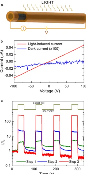
Figure 2. Photoconductivity of selenium microwire and nanowire arrays. Amorphous selenium wires are crystallized via heat treatment and by exposing to organic reagent pyridine. (a) Schematic of the photo-conductance measurement geometry (b) Photo photo-conductance from a selenium microwire in dark and upon white light illumination. (c) Logarithmic increase in photocurrent versus dark current ratio (I/I0) and
reduction in switching times (Δt) with reducing nanowire diameters are observed. The performance increase is attributed to high optical density of selenium, increased surface area-to-volume ratio, and enhanced scattering in the polymer matrix.
produce functional nanostructures. Lastly, we demonstrate logarithmic enhancement of photoconduction from the large-area nanowire arrays after crystallization of the as drawn nanowires (Fig. 2).
We investigated size dependent photoconductivity of selenium micro and nanowire arrays fabricated using the described technique. In a three step drawing process, we
obtained a 56 micron wire, an array of 100×8 micron wires, and an array of 10,000×190 nanometer selenium nanowires. Amorphous wires are crystallized via heat treatment, by annealing above crystallization (Tx=110 °C) but below melting temperature. After crystallization we observe that the conductivity increase up to 10-4 S/cm consistent with bulk selenium conductivities. Step 3 nanowires were chemically crystallized after extraction from the polymer matrix. Electrical gain due to photoconductivity is measured by shining white light (50 W) while applying voltage bias. Photoconductance of the nanowires are observed to be a function of the nanowire number and size in the array. We observe that I/I0 gain (photocurrent vs. dark current) was an order of magnitude large for step 2 wires and two orders of magnitude larger for step 3 wires with respect to the single selenium microwire from the first drawing. The switching between on/off states are also faster with the smaller nanowire sizes. We attribute the logarithmic increase in photoconductance to high absorption of selenium, increased surface area-to-volume ratio, and enhanced scattering of the incoming beam.
Compared with widely employed nano-fabrication techniques, such as chemical synthesis and electrolitography, this method has unique achievements in high-throughput, cost-efficiency global alignment, extended lengths and good uniformity of the nanowires. We expect that the unique geometry, high-throughput and simplicity of the nanofabrication method will attract broad interest and likely to spawn new applications, such as large area nanowire photodetectors, conformal photo-detection, flexible large- area nanowire electronics and photovoltaics.
ACKNOWLEDGMENT
This work was partially supported by State Planning Organization (DPT) and TUBITAK under the Project No. 106G090. M.B. acknowledges support from the Turkish Academy of Sciences Distinguished Young Scientist Award (TUBA GEBIP).
REFERENCES
[1] C. M. Lieber, Z. H. Wang, "Functional Nanowires," MRS Bull. 32, 99, (2007).
[2] Yang, P., Yan, R. & Fardy, M. "Semiconductor Nanowire: What's Next?" Nano Lett. 10, 1529-1536 (2010).
[3] M. Yaman, M Bayindir et al, "Indefinitely-long, uniform nanowire and nanotube arrays," Nature Mater., in press (2011).