Hybrid J
‑Aggregate−Graphene Phototransistor
Ozan Yakar,
†Osman Balci,
‡Burkay Uzlu,
§,∥Nahit Polat,
†Ozan Ari,
⊥Ilknur Tunc,
#Coskun Kocabas,
¶and Sinan Balci*
,††
Department of Photonics, Izmir Institute of Technology, 35430 Izmir, Turkey
‡Department of Physics, Bilkent University, 06800 Ankara, Turkey
§
Advanced Microelectronic Center Aachen, AMO GmbH, Otto-Blumenthal-Strasse 25, 52074 Aachen, Germany
∥Chair of Electronic Devices, RWTH, Aachen University, 52074 Aachen, Germany
⊥
ASELSAN Research Center, Ankara, Turkey
#
Department of Mechanical Engineering, University of Turkish Aeronautical Association, 06790 Ankara, Turkey
¶
School of Materials and National Graphene Institute, University of Manchester, Oxford Rd., Manchester M13 9PL, U.K.
*
S Supporting InformationABSTRACT:
J-aggregates are fantastic self-assembled chromophores
with a very narrow and extremely sharp absorbance band in the visible
and near-infrared spectrum, and hence they have found many exciting
applications in nonlinear optics, sensing, optical devices, photography,
and lasing. In silver halide photography, for example, they have
enormously improved the spectral sensitivity of photographic process
due to their fast and coherent energy migration ability. On the other
hand, graphene, consisting of single layer of carbon atoms forming a
hexagonal lattice, has a very low absorption coe
fficient. Inspired by the
fact that aggregates have carried the role to sense the incident light in silver halide photography, we would like to use
J-aggregates to increase spectral sensitivity of graphene in the visible spectrum. Nevertheless, it has been an outstanding challenge
to place isolated J-aggregate
films on graphene to extensively study interaction between them. We herein noncovalently fabricate
isolated J-aggregate thin
films on graphene by using a thin film fabrication technique we termed here membrane casting (MC).
MC signi
ficantly simplifies thin film formation of water-soluble substances on any surface via porous polymer membrane.
Therefore, we reversibly modulate the Dirac point of graphene in the J-aggregate/graphene van der Waals (vdW)
heterostructure and demonstrate an all-carbon phototransistor gated by visible light. Owing to the hole transfer from excited
excitonic thin
film to graphene layer, graphene is hole-doped. In addition, spectral and power responses of the all-carbon
phototransistor have been measured by using a tunable laser in the visible spectrum. The
first integration of J-aggregates with
graphene in a transistor structure enables one to reversibly write and erase charge doping in graphene with visible light that
paves the way for using J-aggregate/graphene vdW heterostructures in optoelectronic applications.
KEYWORDS:
J-aggregates, graphene, frenkel exciton, membrane casting,
field effect transistor, phototransistor, dirac point,
optoelectronics, photodetector
■
INTRODUCTION
Graphene has received a tremendous amount of interest
because of its exceptional electrical and optical properties
1,2and has found many applications in the optoelectronics area
such as solar cells,
3light-emitting diodes, photodetectors,
4−6lasers,
7optical modulators,
8and infrared camou
flage.
9Owing
to its only 2.3% of light absorption, chemical and thermal
stability, high
flexibility, and one carbon atom thickness (0.345
nm), graphene has been used as a transparent conductor in
photodetectors, solar cells, liquid crystal displays,
field effect
transistors, and light-emitting diodes in
flexible and printable
optoelectronics.
10−15In addition, recently distict
two-dimen-sional nanomaterials have been integrated with graphene into
van der Waals (vdW) heterostructures.
16−18In fact, most of
these applications require controlling the type (n-type or
p-type doping) and density of charge carriers on graphene.
19−22To date, chemical doping,
19,23electrostatic gating,
20,24and
photoinduced doping
25have been frequently used to control
charge density on graphene. Speci
fically, chemical doping is
achieved by chemical compounds or nanoparticles near or in
(substitutional doping) graphene,
23,26electrical doping is
obtained by changing the gate voltages,
22,27and photoinduced
doping is done by placing a light-sensitive chemical compound
near graphene and by using light to excite that chemical
compound.
25,28Developing new ways of reversible and
controllable doping (charge density and types) of graphene
is urgently needed and very crucial for future graphene
optoelectronics since increasing the level of doping in
Received: October 20, 2019
Accepted: December 11, 2019
Published: December 11, 2019
Article
www.acsanm.org Cite This:ACS Appl. Nano Mater. 2020, 3, 409−417
Read License, which permits copying and redistribution of the article for non-commercial scholarly purposes.
Downloaded via BILKENT UNIV on February 12, 2021 at 08:51:32 (UTC).
graphene will signi
ficantly modify optical properties of
graphene; for example, high doping of graphene will extend
graphene plasmon frequencies in the near-infrared region.
29In recent years, photoinduced doping has received a special
interest because (I) photoinduced doping is a dynamic process
where doping level of graphene can be reversibly controlled by
light,
25,28(II) high doping levels can be achieved
∼10
12cm
−2,
30(III) current
flow in the graphene transistor can be
altered by light
“light gating”,
4(IV) graphene-based
photo-detectors working in a broad range of wavelengths and good
responsivity can be achieved,
4,5and (V) p
−n junctions can be
optically and spatially created on graphene.
31Until now,
quantum dots,
4light switchable azobenzene
chromo-phores,
25,28perovskites,
32,33and two-dimensional
nanomateri-als
5,30have been mainly used to e
fficiently photodope
graphene with light. One of the most interesting and
traditional light-sensitive supramolecular self-assembled
struc-tures is J-aggregates,
first observed by Jelly and Scheibe in
1936,
34,35which self-assemble at high concentration and show
a very narrow and intense absorption band, which is shifted to
longer wavelengths relative to the monomer absorption band.
Notably, at high concentration, individual dye molecules
organize in a brickstone work like structure, and thus
J-aggregates can be considered as a two-dimensional
sys-tem.
35−37In fact, J-aggregates were popularly used for spectral
sensitization of photographic processes with silver halides
because of strong light absorption in the visible spectrum.
35Likewise, inspired by the fact that J-aggregates have carried the
role to sense the incident light in silver halide photography, we
herein use J-aggregates to increase spectral sensitivity of
graphene in the visible spectrum and demonstrate a hybrid
J-aggregate
−graphene phototransistor. Until now, J-aggregates
have been widely used in demonstration of polariton lasers,
38solar cells,
39second harmonic generation,
40sensitive and
selective detection of molecules,
41nonlinear optical devices,
42observation of exciton polaritons,
43,44color selective
photo-detectors,
45and synthesis of plexcitonic nanoparticles.
46,47The
recent applications show that J-aggregates could indeed
establish a bridge between the
fields of photonics and
excitonics.
48However, J-aggregates have not been applied in
photodoping of graphene, and thus integration of graphene
with J-aggregate family dyes will open new directions for
graphene optoelectronics in the visible and near-infrared part
of the spectrum.
Owing to the hydrophobicity of polymer transferred
single-layer graphene on a surface, it is very challenging to place a
polar solvent, i.e., water, soluble quantum dots, or dye
molecules on graphene. Previously, to fabricate hybrid
light-sensitive gain medium/graphene heterostructure, spin-coating,
drop-casting, and supramolecular
π−π stacking
28have been
chie
fly used to place molecules and nanomaterials on
graphene.
25It should be noted that although superhydrophilic
and superhydrophobic graphene structures in large area can be
achieved by vertically aligning graphene nanosheets,
49single-layer graphene on a
flat surface synthesized by chemical vapor
deposition and transferred by a polymer, e.g., poly(methyl
methacrylate) (PMMA), shows hydrophobic properties, i.e.,
contact angle of 92
°.
50,51Alternatively, the simple and easy
layer-by-layer (LBL) method
52can be used to create
J-aggregate thin
films on glass or silicon substrates; however, the
method does not work on graphene since aqueous solutions of
cationic and anionic polyelectrolytes used in LBL deposition
do not properly adhere to the graphene surface.
53To
circumvent this problem, we have developed a new thin
film
fabrication technique that we call here membrane casting
(MC) and successfully fabricated a J-aggregate
−graphene
phototransistor gated by visible light (Figure 1). Thanks to
the hole transfer from J-aggregate thin
film to graphene,
graphene is e
ffectively p-doped. The new technique enables us
to reversibly write and erase charge doping in graphene with
visible light. The
first integration of graphene with J-aggregate
dyes will open new avenues in application of graphene in
optoelectronics at visible and near-infrared wavelengths.
■
EXPERIMENTAL SECTION
Graphene (typically several cm2) on copper foils (Mitsui Mining and Smelting Company, Ltd. BI-SBS) was synthesized by the chemical vapor deposition (CVD) technique using methane as a carbon precursor as described in detail previously.9,54The copper foils were cut into small pieces and placed on a quartz holder inside a hollow cylindrical quartz tube in a high-temperature furnace. Briefly, the temperature of the growth chamber wasfirst increased to 1035 °C under theflow of 100 sccm H2gasflow. Afterward, at 1035 °C, CH4
gas with 10 sccmflow rate was introduced for a minute. Subsequently, the reaction chamber was cooled to room temperature in about an hour. Afterward, graphene on copper foils was uniformly coated with light-sensitive polymers, i.e., photoresists (Shipley 1813 photoresist), and annealed at 70°C overnight. Likewise, PMMA can also be used instead of Shipley 1813.54,55First, the copper film was completely etched in 1 M FeCl3aqueous solution. Then, graphene attached to
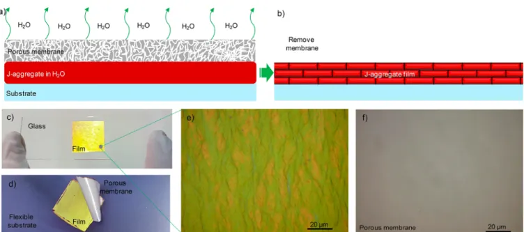
photoresistfilm was transferred to dielectric substrate by heating first at 80°C for a few minutes and then at 110 °C for a minute. Finally, the photoresist film was completely removed from graphene by washing with acetone for several times and finally rinsing with isopropyl alcohol. Raman spectra of samples after graphene transfer onto glass and silicon substrates indicate that graphene is indeed single layer in large area.54 To fabricate flexible graphene devices, graphene was transferred to a 75 μm thick poly(vinyl chloride) substrate by using the hot lamination technique.54 After etching copper foils, the gold metal electrodes were fabricated. A cyanine dye J-aggregate, (5,5′,6,6′-tetrachlorodi(4-sulfobutyl)benzimidazolo-carbocyanine (TDBC), purchased from FEW Chemicals, was used without further purification. To fabricate J-aggregate thin films, a 10 mM TDBC aqueous solution was prepared. In a typical film fabrication, 50 μL of 10 mM TDBC solution was placed between porous polyethylene membrane and a substrate. After 10 min waiting at room temperature, the porous membrane was gently removed from Figure 1.Graphene−J-aggregate hybrid. Schematic representation of thefield effect transistor with the excitonic film, i.e., a phototransistor, under visible light illumination. Graphene layer is transferred on Si3N4
dielectric film and uniformly covered with excitonic thin film fabricated by the membrane casting technique. The size of the J-aggregate thin film is dictated by the porous polymer membrane. Source and drain electrodes are fabricated by thermal evaporation of gold. The red region between the source and drain represents the J-aggregate sample. Incident photons generate electron−hole pairs in the excitonicfilm. The holes transfer from J-aggregate thin film to graphene, and hence graphene is effectively p-doped. The charge density on graphene layer is indeed dynamically modulated by the incident photons impinging on the J-aggregatefilm.
solid J-aggregate film. The porous polyethylene membrane (PEM), which is commonly used as a separator in lithium ion batteries, was purchased from the Gelon LIB Group (Celgard 2730).56In fact, the
membrane is 20μm thick and has a porosity of around 43%. Notably, water molecules pass through the pores of the membrane, and an isolated solid J-aggregate thinfilm was obtained between the porous membrane and substrate. The thickness of the J-aggregate film, measured by a stylus profiler (Dektak-XT, Bruker), is around 150 ± 50 nm. To gate the phototransistor with visible light, a super-continuum laser (Koheras-SuperK Versa) with acousto-optic tunable filter working in the visible and near-infrared spectra was used as a tunable laser light source with a spectral width of around 1 nm. In addition, the laser beams were expanded and collimated to illuminate the entire surface of the transistor. In reflection and transmission measurements, a variable angle spectroscopic ellipsometer (J. A. Woollam, VASE) was used. The dielectric function of the excitonic thin film was measured by using the same ellipsometer. Photo-luminescence (PL) emission measurements of J-aggregate thinfilms were obtained by using Varian Cary Eclipsefluorescence spectropho-tometer. In fact, the excitation wavelengths in PL measurements were varied from 360 to 540 nm with 10 nm increments. While the electrical transport measurements of devices were performed by using a Keithley 2400 source measure unit, the resistance of the J-aggregate/graphene hybrid system was measured by using a Keithley 2000 digital multimeter in an air environment and at room temperature. All electrical and optical measurements were done at ambient conditions.
■
RESULTS AND DISCUSSION
We fabricated the hybrid graphene
−J-aggregate
phototransis-tor and reversibly modulated the Dirac point of graphene. A
schematic representation of the phototransistor (i.e.,
first
discovered by John N. Shive in 1949)
57is shown in
Figure 1
where the vertical arrows mark gating of the transistor with
visible light, and the current
flow between source and drain
electrodes is isreversibly altered by the gate voltages. Chemical
vapor deposition grown graphene on copper substrates was
transferred to silicon substrates for electrical characterization.
Notably, Raman measurements have con
firmed that graphene
on silicon substrate is indeed single layer.
58An optical
microscope (OM) image of a typical large area 2
× 2 cm
2graphene grown via CVD and transferred on a thick dielectric
film is reported in
Figure S1a. Source and drain electrodes
were fabricated by thermally evaporating 100 nm gold on
graphene. It should be noted that graphene on the dielectric
film is evidently discernible in the OM image as shown in
Figure S1b
because of the strong amplitude modulation of
reflection at the air−graphene−dielectric interface.
59The
isolated J-aggregate thin
film uniformly covers the graphene
surface in which the size of the
film is veritably determined by
the porous membrane size in the MC method (Figure S1b).
Electrical measurements have revealed that graphene can be
reversibly doped with incident photons. In the dark condition,
the Dirac point of graphene is at around 30 V, which indicates
that graphene is indeed hole-doped (Figure 2a). Application of
gate voltage to graphene transistor results in accumulation of
charge carriers in graphene, and thus the resistance of graphene
decreases. In fact, the resistance of the device channel reaches
its maximum value at the Dirac point where the carrier
concentration is at a minimum. In actuality, we expect to see
the Dirac point at around 0 V in undoped graphene, but
graphene has an intrinsic hole concentration due to the
adsorbates in contact with graphene.
60Upon illumination with
white light, graphene is heavily hole-doped. Notably, there is a
large shift in Dirac point of graphene under white light
illumination; see the
Supporting Information
for the spectral
distribution of the white-light-emitting diode. Source−drain
current measurements show that the hybrid system produces
photocurrent when illuminated with white light (Figure 2b). It
is evident in the
figure that graphene is effectively p-doped
under the bright condition. Following absorption of incident
photon energies greater than the band gap, J-aggregates on
graphene undergo a transition from the ground state to a
higher electronic state by generating electron
−hole pairs
(Frenkel excitons).
48The absorption of incident photons is
Figure 2.Electrical characterization of hybrid J-aggregate−graphene phototransistor. (a) A graph shows resistance (kΩ) spectra versus applied gate voltages for the bright and dark conditions. Resistance decreases several kiloohms under the visible light illumination because of increase in density of carrier concentration. The Dirac point of graphene can be reversibly tuned by incident photons. (b) Source−drain current as a function of the drain voltage shows increase of the drain current under the visible light illumination. Actually, incident photons generate electron−hole pairs, whereupon holes are transferred to graphene channel. Consequently, holes drift to drain and thus increase the drain current. (c) Schematic representation of the energy level diagram of the J-aggregate−graphene interface. Upon excitation of the J-aggregate, bound states of electrons and holes are created, and subsequently holes are transferred to graphene and electrons are concurrently trapped in the J-aggregate thinfilm. Eventually, the holes lower the Fermi energy of graphene, and hence, in the bright condition, graphene is heavily hole-doped.
followed by nonradiative relaxation of excited electrons to
lower vibrational states, and then the energy (heat) is released
in the process if the electron
−hole recombination is radiative
(nonradiative).
61Meanwhile, the holes can also be transferred
to graphene, which e
fficiently dopes graphene and lowers the
Fermi level of graphene (Figure 2c). Note that previous
observations in PbS quantum dots/graphene hybrids have
shown that graphene is p-doped when PbS quantum dots
absorb incident photons.
4In fact, the holes on the graphene
channel drift toward the drain and thus increase the drain
current while electrons stay in the J-aggregates as it has been
also observed in the PbS
−graphene system.
4Therefore, drain
current increases in the bright condition. Previously, it was
experimentally demonstrated and theoretically calculated that
J-aggregates (e.g., TDBC) have exciton di
ffusion lengths of a
few hundred nanometers, which are more than the exciton
di
ffusion lengths measured in typical organic semiconductor
and quantum dot
films, i.e., around a few tens of
nanome-ters.
62−64In our case, the J-aggregate
film thickness is around
150
± 50 nm, and hence we can safely assume that most of the
generated excitons reach and contribute e
ffective hole doping
of the graphene layer. In addition, to understand the e
ffect of
excitonic thin
film thickness on device performance, we
fabricated J-aggregate
−graphene hybrids on a flexible substrate
(i.e., poly(vinyl chloride) (PVC)) and illuminated the device
from the excitonic thin
film site (front) and graphene site
(back). For optically thick excitonic
films we observed only
resistance variation from the back-illumination. Therefore,
J-aggregate
−graphene transistors on transparent substrates can
be used in back-illumination to eliminate excitonic
film
thickness dependence.
The membrane casting (MC) technique has been used to
yield J-aggregate thin
films on graphene (
Figure 3). Brie
fly, 10
μL of 10 mM TDBC aqueous solution was dropped on a
substrate, and the drop was uniformly covered with porous
polyethylene membrane as shown in the schematic
representa-tion (Figure 3a,b). The substrate and porous membrane
strongly adhere to each other because of the capillary forces.
Owing to the hydrophobic nature of the membrane,
56dye
solution cannot enter the pores of membrane. Note that dye
droplets can be also covered with a glass substrate instead of a
porous membrane, but a glass substrate, nevertheless, blocks
evaporation of water molecules; hence, in the case of a glass
substrate, thin
film formation cannot be achieved. After
evaporation of water in dye solution, the porous polyethylene
membrane is peeled o
ff the rigid and isolated J-aggregate film
on a substrate (Figure 3c
−f). The force needed to peel an
elastic thin
film from a substrate has been extensively studied
and strongly depends on several parameters such as adhesive
surface energy, elastic modulus of the
film, and thickness of the
film.
65Recently, based on these parameters, capillary peeling
has been proposed and used to detach hydrophobic
films from
a substrate.
66Therefore, the interaction between the porous
polymer
film and J-aggregate on the substrate determines the
optical quality of the J-aggregate
film. One important
advantage of the MC technique over other thin
film fabrication
techniques is that water-soluble substances can be assembled
on virtually all kinds of substrate surfaces, i.e., hydrophilic or
hydrophobic, and the size of the
film is absolutely dictated by
the size of the porous membrane. Thus, the graphene layer is
selectively and uniformly coated with an isolated J-aggregate
thin
film as shown in
Figure 3c. In addition, the isolated
excitonic thin
film does not dissolve in acetone, which means
that the excitonic thin
film is compatible with lithographic
processes (details of the micropattern formation using
photolithography will be published elsewhere). In fact,
generating an organic superlattice of J-aggregates on a metal
substrates is very interesting and attractive, for example, for
understanding plexciton mediated energy
flow at nanoscale
dimension
67and localization of incident light below the
di
ffraction limit as well.
68Figure 3.Membrane casting (MC) technique for fabricating J-aggregate thinfilm. (a) Porous polyethylene membrane assists removal of water molecules from the J-aggregate solution located on a substrate. (b) After removal of the porous membrane, the isolated J-aggregate thinfilm is yielded on a substrate. It should be noted here that the size of the membrane dictates thefinal size of the excitonic thin film on the substrate. (c, d, e) Optical microscope images of J-aggregatefilm on a glass (i.e., a rigid substrate) and poly(vinyl chloride) (i.e., a flexible substrate) indicate uniformfilm formation. The excitonic film has a golden appearance. (f) Optical microscope images of porous polyethylene membrane. The porous membrane is strongly hydrophobic, and hence the J-aggregate aqueous solution is not allowed to penetrate inside the pores of the membrane.
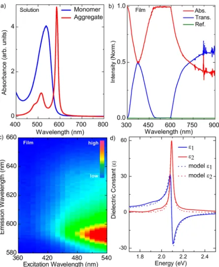
Figure 4. Optical characterization of excitonic thin film. (a) Absorbance spectra of monomer and J-aggregate molecules in water. (b) Transmittance (T), reflectance (R), and absorptance (A) spectra of isolated excitonic thin film fabricated by membrane casting technique (A + R + T = 1). (c) Emission of excitonic thinfilm as a function of excitation wavelength shows broad emission band at around 595 nm. (d) Real (blue line) and imaginary (red line) dielectric constants of isolated J-aggregate thinfilm measured with an spectroscopic ellipsometer. The results of Lorentzfitting model for real and imaginary dielectric constants are also given.
Figure 5.Temporal response of the hybrid J-aggregate/graphene phototransistor in the dark and under illumination. (a) Temporal resistance change of the device at 600 nm and under illumination of 100% power. At full laser power, in less than 3 s about 0.5 kΩ resistance change occurs. Note that the laser is on and off in the red and bright green regions, respectively. (b) Temporal resistance change of the hybrid device as a function of the applied laser power. The dashed lines in the graph indicate when the laser is off.
Optical characterization of the aggregate solution and
J-aggregate thin
films investigated by using absorption and
emission spectroscopy has revealed that J-aggregate thin
films
and aqueous solutions have very broad and narrow absorbance
spectra, respectively, in the visible region while J-aggregates in
thin
films and in aqueous solution have very similar emission
properties (Figure 4). The sharp intense narrow absorption
band (
∼585 nm) at a longer wavelength than monomer peak
(
∼537 nm) is indication of J-aggregate formation in the
solution (Figure 4a). The narrow emission peak at around 600
nm dominates the emission map (see the
Supporting
Information
for the emission map). Owing to the aggregation
of dye molecules in the J-aggregate thin
film, the broad
absorbance peak appears in the visible region (Figure 4b). The
central emission wavelength of the
film is ∼595 nm, which is
red-shifted with respect to the J-aggregate emission in solution,
i.e.,
∼587 nm (
Figure 4c). The real and imaginary dielectric
constant of excitonic thin
film is shown in
Figure 4d. The real
part of the dielectric function is negative at high frequencies,
and thus exciton polaritons can be generated by using the
excitonic thin
film.
68Now, we would like to examine spectral and power
responses of the all-carbon phototransistor by taking a closer
look at its measured resistance variation in the dark and under
laser light illumination. Temporal resistance variation of the
device at 600 nm and 100% laser power as shown in
Figure 5a
indicates that resistance of graphene can be reversibly tuned by
the incident photons. It should be noted that 100% laser power
corresponds to 165
μW/cm
2(see the
Supporting
Informa-tion). At full laser power, in less than 3 s about 0.5 k
Ω
resistance variation occurs. In fact, the rate of the resistance
variation signi
ficantly increases with the increase in the
incident laser power (Figure 5b). Rise and fall times of the
device resistance are not equal to each other, which is most
likely due to the surface trap states in J-aggregate
−graphene
hybrids.
69Furthermore, the detailed photoresponse of the
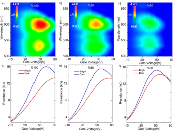
phototransistor at di
fferent laser powers is indicated in
Figure
6. The resistance variation decreases with the applied incident
laser power. At the Dirac point (at around 40 V gate voltages),
the largest resistance variation can be observed (Figure 6a
−c).
Owing to the variation of the laser power with wavelength (see
the
Supporting Information), the resistance variation maps in
Figure 6a
−c are not uniform along the wavelength axis. Along
the gate voltage axis, since the charge density on graphene
varies with the gate voltage, the resistance variation map is not
uniform and represents the location of Dirac point. Indeed,
resistance vs gate voltage graphs demonstrate that the Dirac
point of graphene can be reversibly tuned with the incident
photons. It is obvious in the
figure that the shift in Dirac point
is larger at high laser powers. The charge density on graphene,
which can be deduced from the graphs in
Figure 6d
−f,
increases from 1.5
× 10
12to 4.4
× 10
12cm
−2as the incident
laser power is tuned from 30% to 100%. The critical parameter
indicating the performance of a photodetector is the
photoresponsivity R
p, which is expressed as R
p=
ΔI
p/P
laser=
(I
bright− I
dark)/P
laser= V
sd(1/R
bright− 1/R
dark)/P
laser= V
sd(R
dark− R
bright)/R
darkR
brightP
laser, where I
pis the photocurrent, P
laseris
the laser power, and R is the resistance of graphene in the dark
and bright conditions, respectively. The responsivity of the
phototransistor is calculated to be around
∼20 mA/W for the
device shown in
Figure 6; see the
Supporting Information
for
the laser power dependence of the responsivity.
Figure 6.Photoresponse of the phototransistor. (a, b, c) Photoresponse of the phototransistor at (a) 100%, (b) 50%, and (c) 30% laser powers. The red and blue regions indicate large and small resistance variations, respectively. The resistance variation decreases with the applied incident laser power. Along the gate voltage axis, since charge density on graphene changes with the gate voltage, the map is not uniform and represents the location of Dirac point. (d, e) Resistance vs gate voltage graphs show that the Dirac point of graphene can be reversibly tuned with the applied incident laser power at 600 nm. The shift in Dirac point is larger at high laser powers.
■
CONCLUSION
In conclusion, we have integrated J-aggregate dyes with
graphene and demonstrated an all-carbon phototransistor
gated by incident photons. We can increase the spectral
sensitivity of graphene in the visible spectrum and dynamically
tune the Dirac point of graphene in hybrid J-aggregate
−
graphene structure, and thus the charge density on graphene
can be reversibly tuned by visible light. In addition, we have
developed a novel, facile thin
film fabrication technique we
called here as membrane casting (MC) for noncovalent
assembly of J-aggregates on graphene. The new thin
film
fabrication technique allows thin
film fabrication of
water-soluble nanomaterials and molecules on any surface by using
the porous hydrophobic polyethylene membrane. Therefore,
MC can be used to fabricate thin
films of variety of
water-soluble materials such as proteins, metallic or semiconducting
nanoparticles, graphene oxide, and polymers on desired
substrate surfaces. In the J-aggregate
−graphene structure,
graphene is very sensitive to the visible light. Graphene is
a
ffectively p-doped as confirmed by electrical measurements.
Spectral and power responses of the all-carbon phototransistor
were measured by using a tunable laser. The
first integration of
J-aggregates with graphene in a phototransistor fabricated by a
new thin
film fabrication technique described here enables
reversible writing and erasing of charge doping in graphene
with incident photons that should prove applicable to a wide
range of graphene photonics and optoelectronics applications
in the visible and near-infrared region of the electromagnetic
spectrum.
1,2■
ASSOCIATED CONTENT
*
S Supporting InformationThe Supporting Information is available free of charge at
https://pubs.acs.org/doi/10.1021/acsanm.9b02039.
Synthesis and transfer of graphene; membrane casting;
phototransistor; Figure S1: the graphene−J-aggregate
hybrid; Figure S2: spectral power distribution of laser;
Figure S3: spectral and power photoresponse of the
phototransistor; Figure S4: thermal chemical vapor
deposition system for the synthesis of graphene; Figure
S5: membrane casting an aqueous solution of
J-aggregates onto
flexible substrates; Figure S6: schematic
representation of the phototransistor gated by a tunable
laser; Figure S7: schematic representation of the
phototransistor gated by a white light; Figure S8:
emission maps of the dye solution and the excitonic
thin
film; Figure S9: responsivity (mA/W) of the
phototransistor; Figure S10: Raman spectrum of
graphene (PDF)
■
AUTHOR INFORMATION
Corresponding Author*E-mail:
[email protected].
ORCIDOsman Balci:
0000-0003-2766-2197Burkay Uzlu:
0000-0001-6776-8901Coskun Kocabas:
0000-0003-0831-5552Sinan Balci:
0000-0002-9809-8688 NotesThe authors declare no competing
financial interest.
■
ACKNOWLEDGMENTS
This work has been supported by grants (117F172 and
118F066) from the TUBITAK.
■
REFERENCES
(1) Bonaccorso, F.; Sun, Z.; Hasan, T.; Ferrari, A. C. Graphene photonics and optoelectronics. Nat. Photonics 2010, 4 (9), 611−622. (2) Avouris, P. Graphene: Electronic and Photonic Properties and Devices. Nano Lett. 2010, 10 (11), 4285−4294.
(3) De Arco, L. G.; Zhang, Y.; Schlenker, C. W.; Ryu, K.; Thompson, M. E.; Zhou, C. W. Continuous, Highly Flexible, and Transparent Graphene Films by Chemical Vapor Deposition for Organic Photovoltaics. ACS Nano 2010, 4 (5), 2865−2873.
(4) Konstantatos, G.; Badioli, M.; Gaudreau, L.; Osmond, J.; Bernechea, M.; de Arquer, F. P. G.; Gatti, F.; Koppens, F. H. L. Hybrid graphene-quantum dot phototransistors with ultrahigh gain. Nat. Nanotechnol. 2012, 7 (6), 363−368.
(5) Koppens, F. H. L.; Mueller, T.; Avouris, P.; Ferrari, A. C.; Vitiello, M. S.; Polini, M. Photodetectors based on graphene, other two-dimensional materials and hybrid systems. Nat. Nanotechnol. 2014, 9 (10), 780−793.
(6) Schuler, S.; Schall, D.; Neumaier, D.; Schwarz, B.; Watanabe, K.; Taniguchi, T.; Mueller, T. Graphene Photodetector Integrated on a Photonic Crystal Defect Waveguide. ACS Photonics 2018, 5 (12), 4758−4763.
(7) Zhang, H.; Tang, D. Y.; Knize, R. J.; Zhao, L. M.; Bao, Q. L.; Loh, K. P. Graphene mode locked, wavelength-tunable, dissipative soliton fiber laser. Appl. Phys. Lett. 2010, 96 (11), 111112.
(8) Sun, Z. P.; Martinez, A.; Wang, F. Optical modulators with 2D layered materials. Nat. Photonics 2016, 10 (4), 227−238.
(9) Salihoglu, O.; Uzlu, H. B.; Yakar, O.; Aas, S.; Balci, O.; Kakenov, N.; Balci, S.; Olcum, S.; Suzer, S.; Kocabas, C. Graphene-Based Adaptive Thermal Camouflage. Nano Lett. 2018, 18 (7), 4541−4548. (10) Polat, E. O.; Uzlu, H. B.; Balci, O.; Kakenov, N.; Kovalska, E.; Kocabas, C. Graphene-Enabled Optoelectronics on Paper. ACS Photonics 2016, 3 (6), 964−971.
(11) Di, C. A.; Wei, D. C.; Yu, G.; Liu, Y. Q.; Guo, Y. L.; Zhu, D. B. Patterned graphene as source/drain electrodes for bottom-contact organic field-effect transistors. Adv. Mater. 2008, 20 (17), 3289.
(12) Pang, S. P.; Hernandez, Y.; Feng, X. L.; Mullen, K. Graphene as Transparent Electrode Material for Organic Electronics. Adv. Mater. 2011, 23 (25), 2779−2795.
(13) Polat, E. O.; Balci, O.; Kakenov, N.; Uzlu, H. B.; Kocabas, C.; Dahiya, R. Synthesis of Large Area Graphene for High Performance in Flexible Optoelectronic Devices. Sci. Rep. 2015, 5, 16744.
(14) Wang, Z.; Uzlu, B.; Shaygan, M.; Otto, M.; Ribeiro, M.; Marín, E. G.; Iannaccone, G.; Fiori, G.; Elsayed, M. S.; Negra, R.; Neumaier, D. Flexible One-Dimensional Metal−Insulator−Graphene Diode. ACS Applied Electronic Materials 2019, 1 (6), 945−950.
(15) Uzlu, B.; Wang, Z. X.; Lukas, S.; Otto, M.; Lemme, M. C.; Neumaier, D. Gate-tunable graphene-based Hall sensors on flexible substrates with increased sensitivity. Sci. Rep. 2019, 9, 18059.
(16) Jariwala, D.; Marks, T. J.; Hersam, M. C. Mixed-dimensional van der Waals heterostructures. Nat. Mater. 2017, 16 (2), 170−181. (17) Li, J. H.; Niu, L. Y.; Zheng, Z. J.; Yan, F. Photosensitive Graphene Transistors. Adv. Mater. 2014, 26 (31), 5239−5273.
(18) Zeng, L. H.; Wang, M. Z.; Hu, H.; Nie, B.; Yu, Y. Q.; Wu, C. Y.; Wang, L.; Hu, J. G.; Xie, C.; Liang, F. X.; Luo, L. B. Monolayer Graphene/Germanium Schottky Junction As High-Performance Self-Driven Infrared Light Photodetector. ACS Appl. Mater. Interfaces 2013, 5 (19), 9362−9366.
(19) Das, A.; Pisana, S.; Chakraborty, B.; Piscanec, S.; Saha, S. K.; Waghmare, U. V.; Novoselov, K. S.; Krishnamurthy, H. R.; Geim, A. K.; Ferrari, A. C.; Sood, A. K. Monitoring dopants by Raman scattering in an electrochemically top-gated graphene transistor. Nat. Nanotechnol. 2008, 3 (4), 210−215.
(20) Wang, F.; Zhang, Y. B.; Tian, C. S.; Girit, C.; Zettl, A.; Crommie, M.; Shen, Y. R. Gate-variable optical transitions in graphene. Science 2008, 320 (5873), 206−209.
(21) Zheng, Y.; Ni, G. X.; Toh, C. T.; Tan, C. Y.; Yao, K.; Ozyilmaz, B. Graphene Field-Effect Transistors with Ferroelectric Gating. Phys. Rev. Lett. 2010, 105 (16), 166602.
(22) Schuler, S.; Schall, D.; Neumaier, D.; Dobusch, L.; Bethge, O.; Schwarz, B.; Krall, M.; Mueller, T. Controlled Generation of a p-n Junction in a Waveguide Integrated Graphene Photodetector. Nano Lett. 2016, 16 (11), 7107−7112.
(23) Wei, P.; Liu, N.; Lee, H. R.; Adijanto, E.; Ci, L. J.; Naab, B. D.; Zhong, J. Q.; Park, J.; Chen, W.; Cui, Y.; Bao, Z. A. Tuning the Dirac Point in CVD-Grown Graphene through Solution Processed n-Type Doping with 2-(2-Methoxyphenyl)-1,3-dimethyl-2,3-dihydro-1H-ben-zoimidazole. Nano Lett. 2013, 13 (5), 1890−1897.
(24) Lee, E. J. H.; Balasubramanian, K.; Weitz, R. T.; Burghard, M.; Kern, K. Contact and edge effects in graphene devices. Nat. Nanotechnol. 2008, 3 (8), 486−490.
(25) Kim, M.; Safron, N. S.; Huang, C. H.; Arnold, M. S.; Gopalan, P. Light-Driven Reversible Modulation of Doping in Graphene. Nano Lett. 2012, 12 (1), 182−187.
(26) Coletti, C.; Riedl, C.; Lee, D. S.; Krauss, B.; Patthey, L.; von Klitzing, K.; Smet, J. H.; Starke, U. Charge neutrality and band-gap tuning of epitaxial graphene on SiC by molecular doping. Phys. Rev. B: Condens. Matter Mater. Phys. 2010, 81 (23), 235401.
(27) Singh, A. K.; Uddin, M. A.; Tolson, J. T.; Maire-Afeli, H.; Sbrockey, N.; Tompa, G. S.; Spencer, M. G.; Vogt, T.; Sudarshan, T. S.; Koley, G. Electrically tunable molecular doping of graphene. Appl. Phys. Lett. 2013, 102 (4), 043101.
(28) Joo, P.; Kim, B. J.; Jeon, E. K.; Cho, J. H.; Kim, B. S. Optical switching of the Dirac point in graphene multilayer field-effect transistors functionalized with spiropyran. Chem. Commun. 2012, 48 (89), 10978−10980.
(29) de Abajo, F. J. G. Graphene Plasmonics: Challenges and Opportunities. ACS Photonics 2014, 1 (3), 135−152.
(30) Ju, L.; Velasco, J.; Huang, E.; Kahn, S.; Nosiglia, C.; Tsai, H. Z.; Yang, W.; Taniguchi, T.; Watanabe, K.; Zhang, Y.; Zhang, G.; Crommie, M.; Zettl, A.; Wang, F. Photoinduced doping in heterostructures of graphene and boron nitride. Nat. Nanotechnol. 2014, 9 (5), 348−352.
(31) Wang, H. I.; Braatz, M. L.; Richter, N.; Tielrooij, K. J.; Mics, Z.; Lu, H.; Weber, N. E.; Mullen, K.; Turchinovich, D.; Klaui, M.; Bonn, M. Reversible Photochemical Control of Doping Levels in Supported Graphene. J. Phys. Chem. C 2017, 121 (7), 4083−4091.
(32) Shao, Y. C.; Liu, Y.; Chen, X. L.; Chen, C.; Sarpkaya, I.; Chen, Z. L.; Fang, Y. J.; Kong, J. M.; Watanabe, K.; Taniguchi, T.; Taylor, A.; Huang, J. S.; Xia, F. N. Stable Graphene-Two-Dimensional Multiphase Perovskite Heterostructure Phototransistors with High Gain. Nano Lett. 2017, 17 (12), 7330−7338.
(33) Lee, Y.; Kwon, J.; Hwang, E.; Ra, C. H.; Yoo, W. J.; Ahn, J. H.; Park, J. H.; Cho, J. H. High-Performance Perovskite-Graphene Hybrid Photodetector. Adv. Mater. 2015, 27 (1), 41−46.
(34) Kobayashi, T. J-aggregates; World Scientific: Singapore, 1996; p vii, 228 pp.
(35) Mobius, D. Scheibe Aggregates. Adv. Mater. 1995, 7 (5), 437− 444.
(36) Anantharaman, S. B.; Stöferle, T.; Nüesch, F. A.; Mahrt, R. F.; Heier, J. Exciton Dynamics and Effects of Structural Order in Morphology-Controlled J-Aggregate Assemblies. Adv. Funct. Mater. 2019, 29 (21), 1806997.
(37) Kirstein, S.; Mohwald, H. Exciton Band Structures in 2d Aggregates of Cyanine Dyes. Adv. Mater. 1995, 7 (5), 460−463.
(38) Paschos, G. G.; Somaschi, N.; Tsintzos, S. I.; Coles, D.; Bricks, J. L.; Hatzopoulos, Z.; Lidzey, D. G.; Lagoudakis, P. G.; Savvidis, P. G. Hybrid organic-inorganic polariton laser. Sci. Rep. 2017, 7, 11377.
(39) Sayama, K.; Tsukagoshi, S.; Hara, K.; Ohga, Y.; Shinpou, A.; Abe, Y.; Suga, S.; Arakawa, H. Photoelectrochemical properties of J aggregates of benzothiazole merocyanine dyes on a nanostructured TiO2film. J. Phys. Chem. B 2002, 106 (6), 1363−1371.
(40) Schildkraut, J. S.; Penner, T. L.; Willand, C. S.; Ulman, A. Absorption and second-harmonic generation of monomer and aggregate hemicyanine dye in Langmuir−Blodgett films. Opt. Lett. 1988, 13 (2), 134−136.
(41) Liang, W. L.; He, S. H.; Fang, J. Y. Self-Assembly of J-Aggregate Nanotubes and Their Applications for Sensing Dopamine. Langmuir 2014, 30 (3), 805−811.
(42) Yabushita, A.; Fuji, T.; Kobayashi, T. Nonlinear propagation of ultrashort pulses in cyanine dye solution investigated by SHG FROG. Chem. Phys. Lett. 2004, 398 (4−6), 495−499.
(43) Wang, H.; Wang, H. Y.; Bozzola, A.; Toma, A.; Panaro, S.; Raja, W.; Alabastri, A.; Wang, L.; Chen, Q. D.; Xu, H. L.; De Angelis, F.; Sun, H. B.; Zaccaria, R. P. Dynamics of Strong Coupling between J-Aggregates and Surface Plasmon Polaritons in Subwavelength Hole Arrays. Adv. Funct. Mater. 2016, 26 (34), 6198−6205.
(44) Lidzey, D. G.; Bradley, D. D. C.; Armitage, A.; Walker, S.; Skolnick, M. S. Photon-mediated hybridization of Frenkel excitons in organic semiconductor microcavities. Science 2000, 288 (5471), 1620−1623.
(45) Walker, B. J.; Dorn, A.; Bulovic, V.; Bawendi, M. G. Color-Selective Photocurrent Enhancement in Coupled J-Aggregate/Nano-wires Formed in Solution. Nano Lett. 2011, 11 (7), 2655−2659.
(46) Balci, S. Ultrastrong plasmon-exciton coupling in metal nanoprisms with J-aggregates. Opt. Lett. 2013, 38 (21), 4498−4501. (47) Balci, F. M.; Sarisozen, S.; Polat, N.; Balci, S. Colloidal Nanodisk Shaped Plexcitonic Nanoparticles with Large Rabi Splitting Energies. J. Phys. Chem. C 2019, 123, 26571.
(48) Saikin, S. K.; Eisfeld, A.; Valleau, S.; Aspuru-Guzik, A. Photonics meets excitonics: natural and artificial molecular aggregates. Nanophotonics 2013, 2 (1), 21−38.
(49) Dong, J.; Yao, Z. H.; Yang, T. Z.; Jiang, L. L.; Shen, C. M. Control of Superhydrophilic and Superhydrophobic Graphene Interface. Sci. Rep. 2013, 3, 1733.
(50) Shin, Y. J.; Wang, Y. Y.; Huang, H.; Kalon, G.; Wee, A. T. S.; Shen, Z. X.; Bhatia, C. S.; Yang, H. Surface-Energy Engineering of Graphene. Langmuir 2010, 26 (6), 3798−3802.
(51) Hong, G.; Han, Y.; Schutzius, T. M.; Wang, Y. M.; Pan, Y.; Hu, M.; Jie, J. S.; Sharma, C. S.; Muller, U.; Poulikakos, D. On the Mechanism of Hydrophilicity of Graphene. Nano Lett. 2016, 16 (7), 4447−4453.
(52) DeLacy, B. G.; Qiu, W. J.; Soljacic, M.; Hsu, C. W.; Miller, O. D.; Johnson, S. G.; Joannopoulos, J. D. Layer-by-layer self-assembly of plexcitonic nanoparticles. Opt. Express 2013, 21 (16), 19103−19112. (53) Bradley, M. S.; Tischler, J. R.; Bulovic, V. Layer-by-layer J-aggregate thin films with a peak absorption constant of 10(6) cm(−1). Adv. Mater. 2005, 17 (15), 1881.
(54) Balci, O.; Kakenov, N.; Karademir, E.; Balci, S.; Cakmakyapan, S.; Polat, E. O.; Caglayan, H.; Ozbay, E.; Kocabas, C. Electrically switchable metadevices via graphene. Sci. Adv. 2018, 4 (1), eaao1749. (55) Van Ngoc, H.; Qian, Y.; Han, S. K.; Kang, D. J. PMMA-Etching-Free Transfer of Wafer-scale Chemical Vapor Deposition Two-dimensional Atomic Crystal by a Water Soluble Polyvinyl Alcohol Polymer Method. Sci. Rep. 2016, 6, 1733.
(56) Arora, P.; Zhang, Z. M. Battery separators. Chem. Rev. 2004, 104 (10), 4419−4462.
(57) Shieve, J. N. Photoreistive translating device. US Patent, 1949. (58) Ferrari, A. C.; Meyer, J. C.; Scardaci, V.; Casiraghi, C.; Lazzeri, M.; Mauri, F.; Piscanec, S.; Jiang, D.; Novoselov, K. S.; Roth, S.; Geim, A. K. Raman spectrum of graphene and graphene layers. Phys. Rev. Lett. 2006, 97 (18), 187401.
(59) Roddaro, S.; Pingue, P.; Piazza, V.; Pellegrini, V.; Beltram, F. The optical visibility of graphene: Interference colors of ultrathin graphite on SiO2. Nano Lett. 2007, 7 (9), 2707−2710.
(60) Goniszewski, S.; Adabi, M.; Shaforost, O.; Hanham, S. M.; Hao, L.; Klein, N. Correlation of p-doping in CVD Graphene with Substrate Surface Charges. Sci. Rep. 2016, 6, 22858.
(61) Akselrod, G. M.; Tischler, Y. R.; Young, E. R.; Nocera, D. G.; Bulovic, V. Exciton-exciton annihilation in organic polariton
cavities. Phys. Rev. B: Condens. Matter Mater. Phys. 2010, 82 (11), 113106.
(62) Valleau, S.; Saikin, S. K.; Yung, M. H.; Guzik, A. A. Exciton transport in thin-film cyanine dye J-aggregates. J. Chem. Phys. 2012, 137 (3), 034109.
(63) Lunt, R. R.; Giebink, N. C.; Belak, A. A.; Benziger, J. B.; Forrest, S. R. Exciton diffusion lengths of organic semiconductor thin films measured by spectrally resolved photoluminescence quenching. J. Appl. Phys. 2009, 105 (5), 053711.
(64) Lee, E. M. Y.; Tisdale, W. A. Determination of Exciton Diffusion Length by Transient Photoluminescence Quenching and Its Application to Quantum Dot Films. J. Phys. Chem. C 2015, 119 (17), 9005−9015.
(65) Kendall, K. Thin-film peeling-the elastic term. J. Phys. D: Appl. Phys. 1975, 8 (13), 1449.
(66) Khodaparast, S.; Boulogne, F.; Poulard, C.; Stone, H. A. Water-Based Peeling of Thin Hydrophobic Films. Phys. Rev. Lett. 2017, 119 (15), 154502.
(67) Yuen-Zhou, J.; Saikin, S. K.; Zhu, T.; Onbasli, M. C.; Ross, C. A.; Bulovic, V.; Baldo, M. A. Plexciton Dirac points and topological modes. Nat. Commun. 2016, 7, 11783.
(68) Cacciola, A.; Triolo, C.; Di Stefano, O.; Genco, A.; Mazzeo, M.; Saija, R.; Patane, S.; Savasta, S. Subdiffraction Light Concentration by J-Aggregate Nanostructures. ACS Photonics 2015, 2 (7), 971−979.
(69) Konstantatos, G.; Levina, L.; Fischer, A.; Sargent, E. H. Engineering the temporal response of photoconductive photo-detectors via selective introduction of surface trap states. Nano Lett. 2008, 8 (5), 1446−1450.