E
ffects of Charging and Electric Field on Graphene Oxide
Mehmet Topsakal,
†Hikmet Hakan Gürel,
†and Salim Ciraci*
,‡†UNAM National Nanotechnology Research Center, Institute of Materials Science and Nanotechnology, Bilkent University, 06800
Ankara, Turkey
‡UNAM National Nanotechnology Research Center, Institute of Materials Science and Nanotechnology, and Department of Physics,
Bilkent University, 06800 Ankara, Turkey
ABSTRACT: We present afirst-principles study of various effects of charging and electric field on the oxidation/deoxidation of graphene oxide consisting of only epoxy groups. Wefirst determined the proper basis set, which hinders the spurious spilling of electrons of graphene oxide when negatively charged or exerted by perpendicular electric field, and treated with periodic boundary conditions. We then showed that the electricfield perpendicularly applied to graphene surface provide side-specific functionalization. We found that the bonds between oxygen and graphene are weakened under applied electricfield. For specific values of excess charge or electricfield, an oxygen atom that is normally adsorbed to the bridge site in equilibrium moves to the top site. By directly charging and/or by applying electricfield, one can monitor this migration as well as desorption of the oxygen adatom. In spite of the negative formation energy, an energy barrier prevents individually adsorbed oxygen atoms from forming oxygen molecules. This energy barrier is dramatically weakened upon negative charging or exertion of an electric field. Our results explain why the reduction of graphene oxide can be facilitated by these external effects.
■
INTRODUCTIONDespite a great deal of experimental and theoretical research carried out recently,1−16 the interaction of oxygen with graphene and the resulting oxidation/deoxidation reactions are not fully understood yet. Following the first synthesis of single-layer graphene,17 graphene oxide (GOX) has been the focus of interest because it provided a potential method for the production of large-scale graphene sheets through the reduction of oxidized multilayer graphenes.1,2 Active research to date has concluded that the oxidation and reduction of graphene are, in fact, rather complex and comprise the interplay of various molecules and atoms, such as O, O2, CO2, OH, H,
and H2O. GOX by itself can be obtained through oxidative exfoliation of graphite, which can be visualized as an individual sheet of graphene decorated with epoxy (C−O−C) and hydroxyl (C−OH) groups on both sides and edges. Recently, it has been shown that multilayer GOX produced by oxidizing epitaxial graphene is a metastable material, whose structure and chemistry evolve at room temperature within approximately 1 month.14While maximum oxygen coverage of graphene can be as high as 50%, it is reduced to 38% in equilibrium.14 Nonetheless, domains of graphene monoxide with C/O ratio of unity are attained by the oxidation of both sides.9It is now
well-established that the properties of graphene emerge from its linearly crossing bands at the Fermi level, which undergo dramatic changes upon oxidation,18,20−22even if one does not know yet how the oxidation takes place and what the character of oxygen coverage is. Introducing a band gap, which varies with oxygen coverage, and hence changing semimetallic graphene into a semiconductor, has been an active field of study in graphene-based nanoelectronics.16,22
Intriguing conclusions obtained from recent studies attracted further interest on the seemingly reversible oxidation and deoxidation processes of graphene. Wei et al.20showed that one can write on oxidized graphene by the heated tip of a scanning tunneling microscope (STM), whereby the light-reflecting (semiconducting) places on the oxidized graphene turn to be dark (or become metallic) after they are traced by the tip. This interesting result leading to thermochemical nanolithography is interpreted as the reduction (or deoxidation) of oxidized graphene. In another work by Ekiz et al.,22it is reported that the oxidized surface of graphene can be changed reversibly Received: October 18, 2012
Revised: February 15, 2013 Published: February 18, 2013
between dark and light spots with applied lateral electricfield, which in turn charges the surface between (+) and (−) polarity depending on the direction of the electricfield. Here they also attributed dark (light) spots to metallic (semiconducting) regions on the surface. Additionally, the extend of reduction can be also controlled by the applied electricfield to tune the band gap.22Deoxidized spots can also be achieved underneath the tip of an STM under specific bias.22These results pointout the crucial feature: namely, modification of the properties of graphene by the controlled and reversible reduction/oxidation of GOX, which is realized by charging it positively or negatively or by applying an electricfield to it perpendicularly or laterally. The formation energy related to the oxidation of graphene is negative, and hence graphene cannot be oxidized through oxygen molecules.16,19 Actually, O2 is physisorbed to bare
graphene surface with a very weak binding energy of 58 meV calculated without van der Waals correction, but it rises to 115 meV when the van der Waals correction23is included. Only at defect sites like holes and vacancies can O2dissociate and its constituent oxygen atoms become adsorbed to carbon atoms having lower coordination numbers.19In contrast to O2, the
bonding of free oxygen to graphene is rather strong and varies between 2.43 and 3.20 eV depending on the coverage.16The crucial questions to be addressed are how oxygen atoms can remain strongly bound to graphene despite their negative formation energy and why bound oxygen atoms are prevented from desorption through the formation of oxygen molecules. Recent studies have provided the energy barrier for diffusion of adsorbed O on graphene and for desorption of O through the formation of O2and CO2.
10,16
The objective of this paper is to provide a better understanding of recent experimental studies18,20−22reporting that external agents cause rapid reduction or, conversely, rapid oxidation of graphene oxide. In this context, we investigated the external agents, such as positive or negative charging and electric field applied perpendicular to the graphene layer, that were involved in recent experimental studies20,22 related to reduction/oxidation of graphene oxide. Here we will focus our attention only on oxygen atoms adsorbed to graphene and do not consider other impurities, such as hydroxyl groups and hydrogen adatoms. We performed the calculations for charged graphene oxide by adding a desired amount of excess electrons (for the case of negative charging) or by removing electrons (for the case of positive charging), and both cases are treated with periodic boundary conditions (PBC). We examined also the behavior of oxidized graphene under a perpendicular electricfield. In addition, this paper presents a comprehensive evaluation of the plane wave (PW) and local (atomic orbital, AO) basis sets infirst-principles calculations of charged systems using PBC.
■
METHODOLOGYWe carried out spin-polarized and spin-unpolarized calculations within density functional theory (DFT) using projector-augmented wave potentials.37 The exchange−correlation potential is approximated by generalized gradient approxima-tion using Perdew, Burke and Ernzerhof (PBE) funcapproxima-tional.38 Initially, we used two different basis sets, namely, plane waves (PW) and local basis (AO) sets for reasons explained below, which are applied by usingfirst-principles simulation packages VASP39 and SIESTA,40 respectively. Based on the results derived from the test calculations, all of our conclusions
concerning the effect of the charging and electric field are obtained from AO calculations using SIESTA.40
A plane-wave basis set with kinetic energy cutoff of 500 eV is used in PW calculations.39 Atomic positions and lattice constants are optimized by the conjugate gradient method, where the total energy and atomic forces are minimized. The convergence for energy is chosen as 10−5eV between two steps. An oxygen adatom adsorbed to one side of graphene breaks inversion symmetry, and a net electric-dipole moment is generated perpendicular to the graphene surface. Dipole corrections36are applied in order to remove spurious dipole interactions between periodic images for the neutral calcu-lations.
In AO calculations,40 the eigenstates of the Kohn−Sham Hamiltonian are expressed as linear combinations of numerical atomic orbitals. A 200 Ryd mesh cutoff is chosen and the self-consistent calculations are performed with a mixing rate of 0.1. Core electrons are replaced by norm-conserving, nonlocal Trouiller−Martins pseudopotentials.41The convergence crite-rion for the density matrix is taken as 10−4.
■
THEORETICAL STUDIES OF CHARGED SYSTEMSRecently, the theoretical investigations of charged nanosystems have been an activefield of study. Poloni et al.24studied the interplay between charge doping and intermolecular distance in the polymerization of C60 fullerene chains using AO calculations. They show that the polymerization depends on both the center-to-center distance of fullerenes and the negative doping of the system. In particular, they observed that up to a doping of four electrons per two molecules, the energy barrier, which is related to the formation energy of covalent bonds between fullerenes, progressively decreases. PW calculations using PWSCF code by Attaccalite et al.25proposed a new way of tuning the electron−phonon coupling (EPC) in graphene by changing the deformation potential with electron/hole doping. The doping is simulated by changing the number of electrons in the unit cell. They show that the EPC for highest optical branch at the K-point in BZ acquires a strong dependency on the doping level due to electron−electron correlation. Density functional tight binding method26,27 (DFTB+) has been also used to explore the effective failure limit of graphene with respect to induced anionic charge produced by electron beam or electric current.28It was predicted that grapheneflakes are resistant to high level of charging, posing no problem in the operation of graphene-based electronic devices, but the localized regions were shown to be transformable from sp2
-bonded into sp3-bonded material before the failure limit. Using DMol3 code,29
Ao et al.30 demonstrated that the applied electricfield can significantly facilitate the binding of hydrogen molecules on N-doped graphene through dissociative adsorp-tion and diffusion on graphene surface. By removing the electric field, stored hydrogens on graphene can be released efficiently under ambient conditions when the hydrogen concentration is higher than 0.5 wt %, which indicates that N-doped graphene can be used as a hydrogen storage material with a storage capacity of 6.73 wt %. Assuming that varying the number of electrons in an adatom−graphene system can be used to simulate the effects of gate voltage, Chan et al.31demonstrate the ionization of Li and Co adatoms by doping. The ionization is accompanied by a sharp change in the electrostatic potential of the adatom. These results were consistent with recent STM experiments for Co on graphene.32The exfoliation of graphite under static positive charge is demonstrated by PW
calculations.33 In another PW study carried out with VASP code, Suarez et al.34analyzed the diffusion of oxygen adatoms on graphene and its dependence on the carrier density controlled by a gate voltage. The energy barrier, which is related to the diffusivity of oxygen on graphene, was predicted to be strongly dependent on the carrier density.
Normally, PBC realized by repeating charged supercells has a divergent electric potential energy and has drawbacks and limitations, which have been the subject matter of several studies in the past. Additional background charge of opposite polarity has been added to neutralize the excess charge and hence to achieve the convergence of electronic potential.35,36 Even with this correction, calculations carried out with PBC and plane wave basis sets became strongly dependent on certain parameters of calculations, such as vacuum spacing s between consecutive slabs.
Comparison of Methods Used in the Calculation of Charged Graphene. Before we start to investigate the effects of charging on oxygen-adsorbed graphene, wefirst examine the limitations of the PBC method, where two-dimensional graphene layers separated by large spacing s are repeated periodically along thez-direction. We carried out first-principles PW calculations as well as AO calculations using linear combinations of numerical atomic orbitals, and we investigated the effect of charging on the graphene layer. Throughout the paper,Q > 0 (or surface charge density σ̅ = Q/A in coulombs per square meter,A being the area of the cell) indicates positive charging, or the number of depleted electrons per cell;Q < 0 indicates negative charging, or the number of excess electrons per cell; andQ = 0 is the neutral cell. The (super)cell is made up of (n × n) primitive unit cells of graphene; each supercell comprises 2n2 carbon atoms and 8n2 valence electrons. We
assume that graphene planes, which are repeating periodically along thez-axis, are parallel to the x,y-plane. In Figure 1a−c we present electronic band structures of graphene calculated by PW and AO forQ = +0.2 electron/cell (σ̅ = +0.61 C/m2),Q =
0 electron/cell, andQ = −0.2 electron/cell (σ̅ = −0.61 C/m2) for the primitive cell (n = 1). Further details about the changes in the band structure of graphene upon charging have been discussed in our recent studies.33,42In the case ofQ = +0.2 (σ̅ = +0.61 C/m2), the Fermi level shifts down or the Dirac point
rises for both PW and AO calculations. Accordingly, semi-metallic graphene turns into a hole-doped semi-metallic system.
For the neutral case (Q = 0), band structures calculated using PW and AO are similar. The work function, the minimum energy that must be given to an electron to release it from the plane of graphene, is the difference between the reference vacuum energy and Fermi level. The value of work function extracted from Figure 1b is 4.26 eV, and this is in good agreement with an earlier study.44Briefly, the results calculated using PW and AO are similar. Minute differences originate from different pseudopotentials used in calculations. Moreover, perfect convergences of different basis sets can be achieved only by using very large cutoff values.
As for the case of negative charging withQ = −0.2 e/cell (σ̅ = −0.61 C/m2), the Fermi level shifts up significantly in AO results. In the PW results, the Fermi level shifts up only slightly and then is pinned by the free electron-like parabolic bands touching to the Fermi level; thereafter the position of the Fermi level is practically unaltered with increasing negative charging as shown in Figure 1c. The dramatic difference for the case of Q < 0 between PW and AO results can be understood through the plane-averaged electronic potential along the z-direction, that
is,V̅(z) as described schematically in Figure 1d. In the actual case,V̅(z) passes through a maximum near the surface and goes to−∞ as z → ±∞ at both sides of one single graphene layer, which is charged with Q < 0. Then the electrons in the graphene can spill to vacuum only if they tunnel through tunneling across a wide triangular barrier. The width of the barrier, w, decreases with increasing negative charging. Accordingly, the tunneling current would be negligibly low and excess electrons would practically be trapped in graphene if the value of|Q| is not very high. However, when treated within Figure 1.(a−c) Energy band structures of graphene calculated for (a) Q = +0.2 e/primitive unit cell (σ̅ = +0.61 C/m2), (b) Q = 0 e/ primitive unit cell, and (c)Q = −0.2 e/primitive unit cell (σ̅ = −0.61 C/m2). Left-hand panels are calculated with PW basis set using VASP code; right-hand panels are calculated with AO basis set using SIESTA code. (d) Schematic description of plane-averaged potential of negatively charged graphene,V̅(z), dipping at the center of vacuum spacing and forming a quantum well-like structure. The vacuum spacing between two adjacent graphenes is denoted by s. The triangular potential barrier and its width areΦBandw, respectively. The quantum well confining electrons, which are spilled from charged graphene of PW calculations, is illustrated by blue lines; the well without bound electrons, shown by red lines, corresponds to AO calculations. For one single graphene layer corresponding to the “actual case”, V̅(z → ±∞) → −∞ for s → ∞. (e) Plane-averaged (linear) charge density,λ̅(z), obtained from PW calculations for Q = −0.2 e/cell (σ̅ = −0.61 C/m2) ands = 20 Å. λ̅(z) in full y-axis range is shown in the inset. Here“cell” indicates the primitive unit cell, and s = 20 Å.
PBC, V̅(z) of periodically repeating graphene layers with a vacuum spacings between them can make a dip reminiscent of a quantum well at the center of the spacing as shown in Figure 1d. Under these circumstances, Kohn−Sham Hamiltonian using PW can acquire solutions in this quantum well, which are localized along thez-direction but are free-electron-like in the x,y-plane parallel to graphene. These states form the parabolic bands (kx,ky) plane as shown in Figure 1c. If the
quantum well dips below the Fermi level with increasings or Q, excess electrons in graphene start to be accommodated in these 2D free-electron-like bands. This ends up with the spilling of electrons into the vacuum region. In Figure 1e we present the plane-averaged charge density,λ̅(z), calculated within PW. By integrating λ̅(z) along the z-direction, it is concluded that graphene can keep only−0.09 e/cell (σ̅ = −0.28 C/m2) out of −0.2 e/cell (σ̅ = −0.61 C/m2) excess electrons. The remaining
−0.11 e/cell (σ̅ = −0.33 C/m2) are spilled out into the vacuum,
namely, to the region between two adjacent graphene planes. Clearly, the spilling of excess electrons, which can be normally trapped in graphene, is an artifact of PBC. The amount of excess electrons spilled to the vacuum spacing increases with increasing s and increasing negative charging. While wide s is not convenient because of excessive charge spilling, smalls may prevent excess electrons from spilling into the vacuum at very low negative charging and can yield reasonable solutions as long as the coupling of the adjacent layers is negligible. However, the charge spilling can set in when the negative charging exceeds a threshold value corresponding to the givens.
The dependency of electronic structure and hence the band gap opening ons in PW calculations of silicene (graphene-like Si) under perpendicular electric field has been also reported recently.43 The perpendicular electric field breaks the mirror symmetry ofV̅(z) and gives rise to a sawtooth-like variation. At highE⃗ and large s, electrons of silicene spilling to low-potential site result in a situation above forQ < 0.
In AO calculations, the spurious quantum well-like structure at the middle of vacuum spacing between graphene layers in PBC is devoid of basis set, and hence cannot support the bound electronic states, which shall be localized alongz-direction, but free-electron-like in thex,y-plane, since the local atomic orbitals are placed only at the atomic sites. This is whyV̅(z) calculated by AO does not accommodate excess electrons in its minimum between graphene layers, even if it is further lowered below the Fermi level with increasing s. The behavior of V̅(z) at the proximity of the surface is similar to the actual case, wheres → ∞. Accordingly, excess negative charge is prevented from spilling into the spacing between adjacent graphene layers, and hence remains in graphene, as in the actual case consisting of one single graphene charged byQ < 0.
In contrast to the above shortcomings arising in PW method in treating the negative chargingQ < 0 of graphene using PBC, results obtained by AO and PW agree forQ ≥ 0. For Q < 0, V̅(z) passes through a maximum at the center of s between graphene layers. Accordingly, a method using PBC and plane-wave basis set is not affected significantly by the size of vacuum spacings if Q ≥ 0, as pointed out in ref 42.
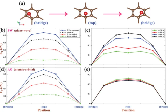
Figure 2.(a) Description of NEB trajectories going from the bridge site to the adjacent bridge site through the top site. Oxygen adatom and carbon atoms of graphene are indicated by a large red sphere and small brown spheres, respectively. (b) Variation of total energiesET, calculated by PW for different values of charging Q at a fixed vacuum spacing s = 20 Å. (c) Variation of ETcalculated by PW for different values of s at a fixed charging Q = −1.0 e/cell (σ̅ = −0.12 C/m2). Panels d and e are the same as panels b and c but are calculated by AO. The calculated total energies at the B-site are set to zero for all cases. Calculations are performed for a single oxygen atom adsorbed to each (5× 5) (super)cell of graphene.
Comparison of Methods Used in the Calculation of Oxygen Adsorbed to Charged Graphene. Having discussed the capacity of plane-wave and local basis sets in representing charged graphene using PBC, we next explore the similar situation for oxygen adatoms. When neutral, a single oxygen is adsorbed at the bridge site of graphene, above the center of the C−C bonds of honeycomb structure. Both PW and AO calculations yield that the bridge site (B-site) is energetically the most favorable adsorption site; the top sites (T-sites, on top of carbon atoms) are not favorable. PW calculations16predicted the binding energies of a single oxygen at the B-site as 2.35, 2.40, 2.43, and 2.43 eV for (2× 2), (3 × 3), (4× 4), and (5 × 5) supercells of graphene, respectively. The binding energy is practically unaltered for supercells larger than (5× 5).16Using AO, we found that the binding energy of oxygen on (5× 5) graphene supercell is 2.34 eV. As calculated from the Bader analysis,45the charge of 0.78 e is transferred from graphene to oxygen atom adsorbed to graphene. The spurious dependence of the energy on the spacing between periodically repeating graphenes,s, is examined by performing NEB (nudged elastic band)46calculations of adsorbed oxygen between two adjacent B-site positions through the T-site position described in Figure 2a. Results obtained from PW and AO calculations using (5 × 5) supercells are presented in Figure 2b−e. According to PW results obtained for s = 20 Å in Figure 2b, the energy difference between the T-site and B-site, ΔE, increases with increasing positive charging (Q > 0) but decreases with increasing negative charging (Q < 0). For example,ΔE > 0.8 eV for Q = +0.5 e/cell (= +0.5/50 e/C atom orσ̅ = +0.06 C/m2), while it is lowered toΔE = 0.1 eV for Q= −1.0 e/cell (σ̅ = −0.12 C/m2). Incidentally, these results are
similar to those obtained by Suarez et al.34using PW. One obtains essentially similar results from AO calculations in Figure 2d. However,ΔE calculated for Q = −1.0 e/cell (σ̅ = −0.12 C/m2) by PW displays a strong dependence on
s in Figure 2c, such that ΔE ∼ 0.1 eV calculated for s = 20 Å
increases to ΔE = 0.32 eV when the spacing between
periodically repeating graphenes is increased tos = 50 Å. The situation with AO results is rather different, as outlined in Figure 2e: Practically,ΔE is not affected by the variation of s. This is due to the fact that the spilling of excess electrons into the spacing between graphene layers is hindered in AO calculations.
In concluding this section, we note the following: (i) The excess charge remaining (or trapped) in graphene predicted by AO calculations is physical for the actual case involving only one single graphene layer as discussed above. (ii) PW calculations correctly predict the charge spilling into the spurious quantum well-like structure in the vacuum region forming for larges as a result of the artifact of PBC. The artifact of PBC sets a limit to the amount of negative charging that can be treated by PW for any given width of the vacuum region. Hence, the PW calculations for negatively charged systems should not be used withs larger than the value where vacuum charging occurs. If the quantity of interest converges before this problem happens, the use of plane-wave codes does not introduce a spurious error as long as the coupling between two layers is negligible. However, since the vacuum charging also increases with increasing negative charging, caution has to be exercised in using small s values, whereby the couplings between adjacent graphene layers can affect the electronic potential near the graphene surface and cause deviations from the actual case. (iii) The spilling of electrons does not occur in
AO calculations even if PBC is used, since local basis orbitals at carbon sites fail to represent states, which can be bound to the quantum well-like potential at the middle of the vacuum spacing. This artifact of AO calculations turns out to be an advantage, which properly cancels out the artifact of PBC. (iv) As described in Figure 1d, near the surface region the electronic potential of one single graphene layer trapping the excess charge in the actual case is close to that obtained by AO calculations using PBC, if the vacuum spacing between adjacent layers hinders the coupling between local basis set at carbon atoms of graphene. Since exponentially decaying atomic orbitals have most of their charge near the surface region, the results obtained from AO calculations for graphene are expected to be very close to the results of the actual case. (v) The above analysis can also be extended to graphene exerted by an electric field perpendicular to it, since a sawtooth-like electronic potential is formed and the excess electrons are spilled to the lower-lying side of electronic potential.
On the basis of the above analysis, we conclude that, in the calculations using PBC and localized atomic orbitals (AO), the spilling of excess electrons into the vacuum region between graphene layers is hindered. Accordingly, results obtained from AO calculations become independent of the vacuum spacings and hence are close to those of the actual case. For these reasons, we carry out AO calculations to reveal the effect of charging and external electricfield in the rest of the paper, and hence, all of our conclusions regarding the effect of charging and electricfield on reduction/oxidation process are obtained by AO calculations using PBC.
■
EFFECTS OF ELECTRIC FIELD AND CHARGING ONA SINGLE OXYGEN ADATOM
The effects of applied electric field and charging are interrelated. Upon the adsorption of oxygen atom, 0.78 electron is transferred from carbon atoms to oxygen in the neutral case. The electric field applied perpendicularly to the graphene, E⃗, which is specified as positive if it is along z-direction (or it is pointing toward oxygen adatom). This electric field induces electronic charge transfer from the adsorbed oxygen to graphene or vice versa if its direction is reversed. Electric field-induced charge transfer modifies the charge distribution and hence affects the physical and chemical properties. Results obtained from this section will enlighten recent experimental studies performed for similar systems.20,22 Interesting effects of electric field on oxygen-adsorbed graphene are summarized in Figure 3. The binding energy of the oxygen adatom increases with applied negative electricfield, which is perpendicular to the surface and pointing in the direction opposite to oxygen. The heighth of oxygen adatom from the graphene plane also increases, even if one expects the opposite trend. This paradoxical situation originates from the definition of the binding energy, Eb, of oxygen adsorbed to graphene, which is given byEb=ET[O] + ET[graphene,E⃗] −
ET[O + graphene, E⃗], in terms of the total energies of single
neutral oxygen atom ET[O], of bare graphene under E⃗,
ET[graphene,E⃗], and of single oxygen adsorbed to graphene
under appliedE⃗, ET[O + graphene,E⃗], all calculated by use of a
(5 × 5) supercell. According to this definition, increasing Eb does not mean that the bond between oxygen and graphene has become stronger. In fact, that h increases with increasing negativeE⃗ implies the opposite situation.
Before we explain this paradoxical situation, wefirst consider charge rearrangements caused by E⃗. Induced charge transfer
depends on the direction of E⃗. In Figure 4 we present the effects of applied perpendicular electric field on the charge distribution and potential energy V̅(z). An electric field E⃗ =
−1.0 V/Å transfers electrons from the bottom side to the upper side of the graphene and also causes further transfer of carbon electrons to oxygen adatom as shown in Figure 4b. At the end, the total energy of the whole system increases. This effect creates an interesting situation also for the bare graphene by breaking the projection symmetry between its two sides. The direction of electron transfer is reversed when the direction of the applied electric field is reversed. Accordingly, one can monitor various properties of bare graphene, in particular its chemical activity, by applying perpendicular electric field and hence by modifying electron concentration at both sides as seen in Figure 4c.
The self-consistent potential energy averaged on the planes perpendicular toz-axis, V̅(z), is presented in Figure 4d. Within PBC, V̅(z) displays a sawtooth behavior. The form of the potential suggests interesting situations for both sides of graphene. For example, one can monitor the work function on both sides. Side-specific effects induced by perpendicular electric field are pronouced in single-layer honeycomb structures consisting of two or three atomic planes, such as silicene,43,47,48 single-layer transition-metal dichalcogenides,49 and graphene bilayer.
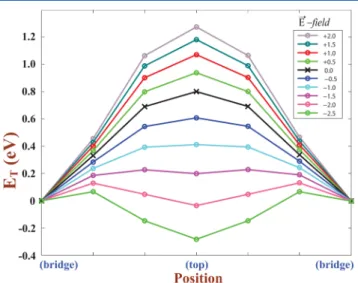
The effect of applied perpendicular electric field on the calculated total energies of oxygen adsorbed at different sites on the NEB path between two adjacent B-sites through the T-site is presented in Figure 5. The difference of total energy ΔE,
between oxygen adsorbed at the T-site and B-site, is as large as ∼1.2 eV for E⃗ = +2.0 V/Å. However, when the direction of E⃗ is reversed,ΔE decreases and becomes even negative for E⃗ = −2.0 V/Å. This is a dramatic effect and is expected to bear on the reduction/oxidation of graphene surfaces. Since the energy barrier between the B-site and T-site can be modified by the applied electricfield, the monitoring of oxygen diffusion at the graphene surface will be possible through applied electricfield. We note that the magnitudes of the electricfields of 1−2 V/Å are high but they are in the range that can be applied at least for short times.50
Figure 3.Variation of binding energyEb, oxygen adatom, and heighth from the graphene plane with electricfield E⃗, applied perpendicular to the graphene plane.E⃗ is taken as positive if it is along z-direction (or it is pointing toward oxygen adatom) and vice versa. (Results are obtained from AO calculations using PBC.)
Figure 4. (a) Atomic configuration showing a single oxygen atom adsorbed at the B-site of a (5× 5) graphene supercell with red and brown spheres indicating oxygen adatom and carbon atoms of graphene, respectively. Thexy plane coincides with the atomic plane of bare graphene, andz-direction is perpendicular to graphene. (b, c) Difference charge density Δρ for the electric field (b) antiparallel (E⃗ < 0) and (c) parallel (E⃗ > 0) to z-direction. Yellow (blue) isosurfaces indicate electron accumulation (depletion) induced byE⃗ applied in different directions. (d) Self-consistent field potential energy averaged on the planes perpendicular toz-axis throughout the supercell, V̅(z), for the casesE⃗ = 0, E⃗ < 0, and E⃗ > 0. (Results are obtained from AO calculations using PBC.)
Figure 5. Variation of total energy ET of a single oxygen atom adsorbed to each (5 × 5) graphene supercell under applied perpendicular electricfields E⃗ on a NEB path between two adjacent B-sites through a T-site. The total energy at the B-site is set to 0 for all cases. The unit ofE⃗ is volts per angstrom. (Results are obtained from AO calculations using PBC.)
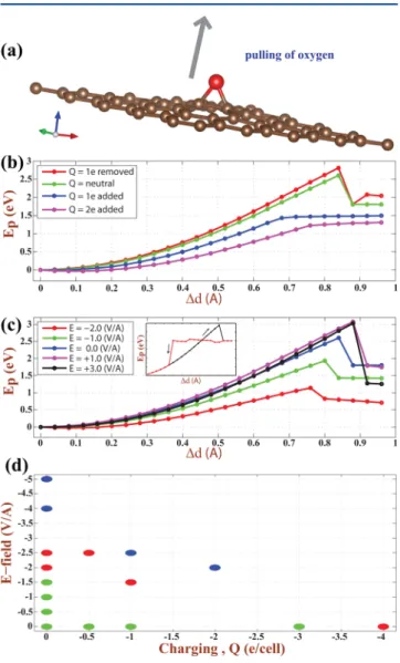
We now resolve the above paradoxical situation, namely, that the equilibrium oxygen graphene distance h increases with increasingEbas shown in Figure 3 and develop a criterion for
the strength of bond between graphene and oxygen adatom. To this end, we consider the system consisting of (5× 5) graphene supercells with a single oxygen adatom, which are either charged byQ or under a perpendicular electric field E⃗ as shown in Figure 6a. We calculated the optimized total energies of this system while oxygen adatom is pulled along z-direction perpendicular to the plane of graphene. For each fixed value
Δd of oxygen adatom from its equilibrium height h, carbon atoms around oxygen adatom are relaxed, while the rest of the atoms arefixed to prevent graphene from displacement. These analyses are continued by varyingΔd for different values of Q [e per (5× 5) cell] and for different values of E⃗ perpendicular to the graphene plane.
The variation of the total energies with pulling Δd are plotted in Figure 6 panels b and c for different values of Q and E⃗, respectively. For the sake of comparison, we also included the pulling curves forQ = 0 and E⃗ = 0. These figures convey interesting features regarding the effects of either charging or applied perpendicular electricfield on the strength of the bond between graphene and oxygen adatom: Normally, the energy associated with pullingEp = ET[O + graphene, Q, E⃗, Δd] −
ET[O + graphene,Q, E⃗, Δd = 0] increases with increasing Δd,
since the system is strained and pulled upward. Eventually it passes through a maximum value denoted by Ep* and drops
suddenly at about 0.8 <Δd < 0.9 Å. Our analysis suggests that Ep* can be taken as a measure for the strength of the bond
between oxygen adatom and graphene. We note that Ep*,
namel,y the energy barrier to pull out the adsorbed oxygen adatom from graphene surface, is∼2.60 eV for both Q = 0 and E⃗ = 0. This energy is consistent with the binding energy calculated for the bridge site. An interesting feature of the present analysis is thatEp* is strongly dependent on charging
and electricfield. While Ep* increases with Q > 0, it decreases
dramatically for Q < 0. For example, Ep* = 1.46 eV for Q =
−1.0 e/cell (or −0.02 e/carbon atom or σ̅ = −0.12 C/m2).
Similarly, Ep* can be as low as ∼1.14 eV under the
perpendicular electric field E⃗ = −2 V/Å. As shown by inset in Figure 6c, a bistability occurs if oxygen atom moves in the reverse direction and hence approaches to the graphene from Δd > 1.0 Å. Notably, for Q < 0, the Ep curve does not
experience a sharp fall passing its maximum value. This is related to the excess charge on oxygen atom. These are important results and demonstrate that it is easier to desorb oxygen adatoms from graphene by negatively charging or by applying perpendicular electricfield. Under high local charging and local electricfield, which can be attained by the sharp tip of a scanning tunneling microscope or by a gate voltage, the reduction of GOX through the desorption of O adatoms can be achieved.
Since the negative charging or negative perpendicular electric field both weaken the bond between oxygen and graphene and hence lower Ep*, we next explore their effects on the bond
between graphene and oxygen adatom when they both coexist. Thus the negative E⃗ of different magnitudes exerts on a negatively charged system consisting of a single oxygen adatom adsorbed to each (5× 5) supercell of graphene. We found that effects the same as in Figure 6b,c are attained by applying relatively lower electric field when the system is negatively charged. In particular, adsorbed oxygen moves high above graphene and becomes weakly bound under the electricfield E⃗ =−2.5 V/Å if the whole system is charged by Q = −1.0 e/cell (orσ̅ = −0.12 C/m2). We note that this value is much smaller than the electricfield required for desorption of oxygen from a neutral system. In Figure 6d we schematically show different positions of oxygen adatom (bridge- and top-site and moved away from graphene for desorption) occurring under different values of negativeE⃗ and negative Q.
Figure 6.Variation of the pulling energyEpof a single oxygen adatom adsorbed to each (5 × 5) supercell of graphene charged by Q or exerted by E⃗ with pulling distance along the z-axis, Δd from its equilibrium heighth. (a) Atomic configuration. Red (large) and brown (small) spheres indicate oxygen and carbon atoms, respectively. (b) Variation ofEpwithΔd, along z-axis for different charging values Q. (c) Variation ofEpwithΔd, along z-axis for different applied electric fields E⃗. All cases have their own equilibrium heights h. The maximum value of the pulling energy for each case is specified by Ep*. As shown by inset for the case ofQ = 0 and E⃗ = 0, a bistability occurs when oxygen atom approaches graphene from a long distance. (d) Positions of adsorbed oxygen atom under different values of electric field E⃗ and/ or chargingQ. Green, red, and blue dots indicate respectively oxygen atom adsorbed to the bridge site, adsorbed to the top site, and desorbed by moving away from graphene plane. (Results are obtained from AO calculations using PBC.)
■
FORMATION OF OXYGEN MOLECULEHaving examined the binding energy, binding site, and diffusion of single oxygen adatoms and their variation with charging and applied electric field, we next consider the formation of O2,
which can be essential in deoxidation. Since single oxygen adatom adsorbed to graphene has negative formation energy, one cannot expect that O2molecule dissociates into two atomic
oxygens, both adsorbed to graphene. However, O2molecules
can dissociate at the edges of vacancy defects or holes and subsequently the constituent atomic oxygens are adsorbed to carbon atoms with lower coordination.19In view of the negative formation energy, one normally expects that two oxygen atoms adsorbed individually to graphene can readily form O2 in an exothermic process when two atoms are in close proximity. Therefore, the interaction of two oxygen adatoms on graphene is essential for the formation of O2. In Figure 7a we examined
O−O interaction for Q < 0 and E⃗ = 0 while one O is at the position identified as p and marked by the arrow as shown by inset, and the other one is diffusing from a distant bridge site identified as a. Initially, the interaction between them is weak, but it develops as one O atom is migrating from a toward p through b, c, and d positions. Here a and c correspond to the bridge sites and b and d to the top sites. Here we consider three situations, which are illustrated by three curves denoted I, II, and III. For curve I, the x- and y-coordinates of all carbon atoms of graphene are kept fixed but their z-coordinates are relaxed as thefirst O adatom migrates from position a to the second O at position p. While thefirst O is forced to migrate through the path of the minimum energy barrier by optimizing its height from graphene, the second O is fully relaxed.
Overcoming the barrier of ∼3.3 eV corresponding to
configuration K, O2 is desorbed at G. Curve I is similar to the curve in Figure 5c of ref 16 calculated by the PW method . For curve II, only one carbon atom out of 72 in the supercell is fixed to prevent underlying graphene from displacing in the course of forced migration of thefirst O adatom. A relatively smaller barrier of ∼2.3 eV develops between d and H, and eventually one O adatom is desorbed once H is overcome at L. Apparently curves I and II are associated with high energy barriers for the desorption of O2or single oxygen atom from
GOX. A different migration path is followed for curve III: Once thefirst O adatom arrived at position d, it is fixed there while the second O adatom at position p is forced to the top site at position e. To attain thefinal configuration J, an energy barrier of 1.3 eV from position c has to be overcame. After J, two O adatoms form O2and desorb from graphene. Clearly, this path described by curve III has a much lower barrier than those of configurations K and H. The energy barriers of curves I−III are lowered with negative charging.
Larciprete et al.10pointed out a dual path described by inset A in Figure 7b, which allows two O adatoms at the bridge sites to move along C−C bonds toward to adjacent top sites. They calculated the energy barrier to be 1.13 eV using PW method and found that it is in good agreement with temperature-programmed desorption (TPD) data. They observed significant O2desorption at∼500 K during the thermal annealing of low oxygen density GOX. Here, we first examine the low-energy-barrier dual path proposed by Larciprete et al.10and calculate the energy barrier forQ < 0 and E⃗ = 0 using the AO method by relaxing all atoms in the supercell except one carbon atom to hinder the displacement of graphene layer. In Figure 7b we present the energy variation of the dual path corresponding to
curve I through A, B, C, and D configurations shown by inset. The energy barrier at B configuration is rather low as compared to K and H configurations in Figure 7a. Overcoming an energy barrier of 0.8 eV, two O adatoms become attached to two adjacent top sites of graphene described as configuration C. The energy barrier calculated by AO method is∼0.3 eV lower than predicted by Larciprete et al.,10 perhaps due to the different parameters of calculations and different basis set. If one of these O atoms is forced toward the other one, an energy barrier of 0.4 eV develops between C and D. The formation of O2 and desorption is achieved at E when D is overcame. A different path specified as curve II in Figure 7b goes to F from C, where one of the O adatoms of configuration C is raised. This way, the formation of O2 is attained without an energy
Figure 7.Interaction between two oxygen adatoms (epoxy groups) at close proximity. (a) Variation of the interaction energy between two oxygen adatoms for three different cases represented by curves I−III associated with a single path. Calculations are carried out for a rectangular supercell consisting of 72 carbon atoms and two oxygen adatoms. Details are given in the text. (Top inset) Isosurface charge densities of C−C bonds and positions of two oxygen adatoms in the course of migration. (Bottom inset) O2and O desorption from various configurations. (b) Variation of the interaction energy between two oxygen adatoms involving dual paths, presented by curves I and II. (Insets) Relevant atomic configurations A−F associated with dual paths and ending with O2desorption. Curves I and II were modified under excess electronic charge (Q = −4 e/supercell or σ̅ = −0.332 C/ m2; Curve III) and applied electric field (E⃗ = −2 V/Å; Curve IV). (Results are obtained from AO calculations using PBC.)
barrier after configuration C. The atomic configurations corresponding to various stages are described by insets.
Having discussed two paths with low energy barrier leading to the formation of O2from GOX, we next examine how these
barriers are affected by external agents such as negative charging and applied electricfield. When charged by Q = −4 e/supercell (σ̅ = −0.332 C/m2), the energy variation of curves I and II is
modified as presented by curve III in Figure 7b. Two oxygen adatoms migrating from configuration A toward configuration C encounter a small energy barrier of∼0.1 eV. This is a really small barrier, which can be further lowered or completely suppressed with increasing excess electrons. The application of the electricfield of E⃗ = −2 V/Å perpendicular to the plane of graphene induces a similar effect shown by curve IV: While the barrier of 0.8 eV at B is suppressed, a small barrier of∼0.2 eV near C appears. The energy barrier in curves III and IV is rather small and explains why GOX can easily be deoxidized under external effects.20,22
■
DISCUSSIONS AND CONCLUSIONSIn order to understand recent experimental works reporting reduction of GOX by charging or by applying electricfield, we investigated the effects of these external agents on single oxygen adatoms on graphene. To separate their possible effects on the reduction process from those of hydroxyl groups, here we consider only the epoxy groups. First, we discussed the limitations and artifacts of methods using plane-wave (PW) and local orbital (AO) basis sets within periodic boundary conditions in treating the systems that are either charged or subjected to perpendicular electric field. While both methods have been successful in treating the atomic and electronic structure of various neutral or positively charged adatom− surface complexes, AO calculations hindering the spurious vacuum charging within PBC are found to be appropriate to treat the systems that are either negatively charged or are exerted by a perpendicular electric field. It appears that an artifact of AO calculations cancels out another artifact of PBC. Our related analyses are believed to be very valuable for future theoretical studies including excess charge and electricfield.
Determining that AO calculations can provide the proper treatment of one single graphene layer, which is charged negatively or subjected to a perpendicular electric field, we carried out structure-optimized, self-consistentfield calculations under specific constraints and NEB calculations between well-defined initial and final configurations. We found that the strength of the bond between graphene and oxygen adatom is weakened with negative charging and/or with perpendicular electricfield applied in the direction opposite to oxygen. With negative perpendicular electricfield and negative charging both coexisting in the system, the desorption and hence reduction of GOX can take place much more easily. Despite the negative formation energy, the formation of oxygen molecule from individual oxygen adatoms adsorbed to graphene is hindered by the energy barriers of 0.8−1.3 eV. The calculated energy barriers are significantly lower than the sum of the binding energies of two single oxygen adatoms due to the concerted action. In this respect, we note the possibility of another reaction path with an even lower energy barrier.
In conclusion, we showed that the calculated energy barriers on various reaction paths are dramatically lowered by charging the system with excess electrons or by applying a perpendicular electricfield. This explains why the reduction of GOX through desorption of oxygen or O2is facilitated as reported by earlier
experimental studies. Notably, perpendicular electricfield can be used also for side-specific functionalization of single-layered and multilayered nanostructures.
■
AUTHOR INFORMATIONCorresponding Author *E-mail [email protected]. Notes
The authors declare no competingfinancial interest.
■
ACKNOWLEDGMENTSWe acknowledge useful and stimulating discussions with Professor A. Dana and O. Ekiz. H.H.G. acknowledges also the support of TUBITAK-BIDEB. Part of the computational resources has been provided by TUBITAK ULAKBIM, High Performance and Grid Computing Center (TR-Grid e-Infrastructure) and UYBHM at Istanbul Technical University through Grant 2-024-2007.
■
REFERENCES(1) Sniepp, H. C.; Li, J.-L.; McAllister, M. C.; Sai, H.; Herrera-Alonso, M.; Adamson, D. H.; Prud’homme, R. K.; Car, R.; Saville, D. A.; Aksay, I. A. Functionalized single graphene sheets derived from splitting graphite oxide.J. Phys. Chem. B 2006, 110, 8535−8539.
(2) Li, J.-L.; Kudin, K. N.; McAllister, M. J.; Prudhomme, R. K.; Aksay, I. A.; Car, R. Oxygen-driven unzipping of graphitic materials. Phys. Rev. Lett. 2006, 96, No. 176101.
(3) Boukhvalov, D. W.; Katsnelson, M. I. Modeling of graphite oxide. J. Am. Chem. Soc. 2008, 130, 10697−10701.
(4) Yan, J.; Xian, L.; Chou, M. Y. Structural and electronic properties of oxidized graphene.Phys. Rev. Lett. 2009, 103, No. 086802.
(5) Yan, J.-A.; Chou, M. Y. Oxidation functional groups on graphene: Structural and electronic properties. Phys. Rev. B 2010, 82, No. 125403.
(6) Wang, L.; Sun, Y. Y.; Lee, K.; West, D.; Chen, Z. F.; Zhao, J. J.; Zhang, S. Stability of graphene oxide phases from first-principles calculations.Phys. Rev. B 2010, 82, No. 161406.
(7) Bagri, A.; Mattevi, C.; Acik, M.; Chabal, Y. J.; Chhowalla, M.; Shenoy, V. B. Structural evolution during the reduction of chemically derived graphene oxide.Nat. Chem. 2010, 2, 581−587.
(8) Xiang, H. J.; Wei, S.-H.; Gong, X. G. Structural motifs in oxidized graphene: A genetic algorithm study based on density functional theory.Phys. Rev. B 2010, 82, No. 035416.
(9) Mattson, E. C.; Pu, H.; Cui, S.; Schofield, M. A.; Rhim, S.; Lu, G.; Nasse, M. J.; Ruoff, R. S.; Weinert, M.; Gajdardziska-Josifovska, M.; Chen, J.; Hirschmugl, C. J. Evidence of nanocrystalline semi-conducting graphene monoxide during thermal reduction of graphene oxide in vacuum.ACS Nano 2011, 5, 9710−9717.
(10) Larciprete, R.; Fabris, S.; Sun, T.; Lacovig, P.; Baraldi, A.; Lizzit, S. Dual path mechanism in the thermal reduction of graphene oxide.J. Am. Chem. Soc. 2011, 133, 17315−17321.
(11) Pei, S.; Cheng, H. The reduction of graphene oxide.Carbon 2012,50, 3210−3228.
(12) Mao, S.; Pu, H.; Chen, J. Graphene oxide and its reduction: Modeling and experimental progress.RSC Adv. 2012, 2, 2643−2662. (13) Huang, H.; Li, Z.; She, J.; Wang, W. Oxygen density dependent band gap of reduced graphene oxide. J. Appl. Phys. 2012, 111, No. 054317.
(14) Kim, S.; Zhou, S.; Hu, Y.; Acik, M.; Chabal, Y. J.; Berger, C.; de Heer, W.; Bongiorno, A.; Riedo, E. Room-temperature metastability of multilayer graphene oxide films.Nat. Mater. 2012, 11, 544−549.
(15) Sun, T.; Fabris, S. Mechanisms for oxidative unzipping and cutting of graphene.Nano Lett. 2012, 12, 17−21.
(16) Topsakal, M.; Ciraci, S. Domain formation on oxidized graphene.Phys. Rev. B 2012, 86, No. 205402.
(17) Novoselov, K.; Geim, A.; Morozov, S.; Jiang, D.; Zhang, Y.; Dubonos, S.; Grigorieva, I.; Firsov, A. Electric field effect in atomically thin carbon films.Science 2004, 306, 666−669.
(18) Dikin, D. A.; Stankovich, S.; Zimney, E. J.; Piner, R.; Dommett, G. H. B.; Evmenenko, G.; Nguyen, S. T.; Ruoff, R. S. Preparation and characterization of graphene oxide paper.Nature 2007, 448, 457−460. (19) Topsakal, M.; Sahin, H.; Ciraci, C. Graphene coatings: An efficient protection from oxidation.Phys. Rev. B 2012, 85, No. 155445. (20) Wei, Z.; Wang, D.; Kim, S.; Kim, S.-Y.; Hu, Y.; Yakes, M. K.; Laracuente, A. R.; Dai, Z.; Marder, S. R.; Berger, C.; King, W. P.; de Heer, W. A.; Sheehan, P. E.; Riedo, E. Nanoscale tunable reduction of graphene oxide for graphene electronics. Science 2010, 328, 1373− 1376.
(21) Zhou, Y.; Bao, Q.; Varghese, B.; Tang, L. A. L.; Tan, C. K.; Sow, C.-H.; Loh, K. P. Microstructuring of graphene oxide nanosheets using direct laser writing.Adv. Mater. 2010, 22, 67−71.
(22) Ekiz, O. O.; Urel, M.; Guner, H.; Mizrak, A. K.; Dana, A. Reversible electrical reduction and oxidation of graphene oxide.ACS Nano 2011, 5, 2475−2482.
(23) Grimme, S. Semiempirical GGA-type density functional constructed with a long-range dispersion correction. J. Comput. Chem. 2006, 27, 1787.
(24) Poloni, R.; Miguel, A. S.; Fernandez-Serra, M. V. A first-principles study of the effect of charge doping on the 1D polymerization of C60.J. Phys.: Condens. Matter 2012, 24, No. 095501. (25) Attaccalite, C.; Wirtz, L.; Lazzeri, M.; Mauri, F.; Rubio, A. Doped graphene as tunable electron-phonon coupling material.Nano Lett. 2010, 10, 1172−1176.
(26) Aradi, B.; Hourahine, B.; Frauenheim, T. DFTB+, a sparse matrix-based implementation of the DFTB method.J. Phys. Chem. A 2007,111, 5678−5684.
(27) Elstner, M.; Porezag, D.; Jungnickel, G.; Elsner, J.; Haugk, M.; Frauenheim, Th.; Suhai, S.; Seifert, G. Self-consistent-charge density-functional tight-binding method for simulations of complex materials properties.Phys. Rev. B 1998, 58, 7260−7268.
(28) Bernard, A. S.; Snook, I. K. Transformation of graphene into graphane in the absence of hydrogen.Carbon 2010, 48, 981−987.
(29) Delley, B. An all-electron numerical method for solving the local density functional for polyatomic molecules.J. Chem. Phys. 1990, 92, 508−517.
(30) Ao, Z. M.; Hernandez-Nieves, A. D.; Peeters, F. M.; Lia, S. The electric field as a novel switch for uptake/release of hydrogen for storage in nitrogen doped graphene.Phys. Chem. Chem. Phys. 2012, 14, 1463−1467.
(31) Chan, K. T.; Lee, H.; Cohen, M. L. Gated adatoms on graphene studied with first-principles calculations. Phys. Rev. B 2011, 83, No. 035405.
(32) Brar, V. W.; Decker, R.; Solowan, H.-M.; Wang, Y.; Maserati, L.; Chan, K. T.; Lee, H.; Girit, C. O.; Zettl, A.; Louie, S. G.; Cohen, M. L.; Crommie, M. F. Gate-controlled ionization and screening of cobalt adatoms on a graphene surface.Nat. Phys. 2011, 7, 43.
(33) Topsakal, M.; Ciraci, S. Static charging of graphene and graphite slabs.Appl. Phys. Lett. 2011, 98, No. 131908.
(34) Suarez, A. M.; Radovic, L. R.; Bar-Ziv, E.; Sofo, J. O. Gate-voltage control of oxygen diffusion on graphene.Phys. Rev. Lett. 2011, 106, No. 146802.
(35) Leslie, M.; Gilan, N. J. The energy and elastic dipole tensor of defects in ionic crystals calculated by the supercell method.J. Phys. C 1985,18, 973−975.
(36) Makov, G.; Payne, M. C. Periodic boundary conditions in ab initio calculations.Phys. Rev. B 1995, 51, 4014−4022.
(37) Blochl, P. Projector augmented-wave method.Phys. Rev. B 1994, 50, 17953−17979.
(38) Perdew, J. P.; Burke, K.; Ernzerhof, M. Generalized gradient approximation made simple.Phys. Rev. Lett. 1996, 77, 3865−3868.
(39) Kresse, G.; Furthmuller, J. Efficient iterative schemes for ab initio total-energy calculations using a plane-wave basis set.Phys. Rev. B 1996,54, 11169−11186.
(40) Soler, J. M.; Artacho, E.; Gale, J. D; Garcia, A.; Junquera, J.; Ordejon, P.; Sanchez-Portal, D. The SIESTA method for ab initio order-n materials simulation.J. Phys.: Condens. Matter 2002, 14 (11), 2745−2779.
(41) Troullier, N.; Martins, J. L. Efficient pseudopotentials for plane-wave calculations.Phys. Rev. B 1991, 43, 1993.
(42) Topsakal, M.; Ciraci, S. Effects of static charging and exfoliation of layered crystals.Phys. Rev. B 2012, 85, 045121.
(43) Drummond, N. D.; Zolyomi, V.; Falko, V. I. Electrically Tunable band gap in silicene.Phys. Rev. B 2012, 85, No. 075423.
(44) Chan, K. T.; Neaton, J. B.; Cohen, M. L. First-principles study of metal adatom adsorption on graphene. Phys. Rev. B 2008, 77, No. 235430.
(45) Henkelman, G.; Arnaldsson, A.; Jónsson, H. A Fast and robust algorithm for Bader decomposition of charge density.Comput. Mater. Sci. 2006, 36, 254−260.
(46) Sheppard, D.; Terrell, R.; Henkelman, G. Optimization methods for finding minimum energy paths. J. Chem. Phys. 2008, 128, No. 134106.
(47) Cahangirov, S.; Topsakal, M.; Akturk, E.; Sahin, H.; Ciraci, S. Two- and one-dimensional honeycomb structures of silicon and germanium.Phys. Rev. Lett. 2009, 102, No. 236804.
(48) Sahin, H.; Cahangirov, S.; Topsakal, M.; Bekaroglu, E.; Akturk, E.; Senger, R. T.; Ciraci, S. Monolayer honeycomb structures of group-IV elements and III-V binary compounds: First-principles calculations. Phys. Rev. B 2009, 80, No. 155453.
(49) Ataca, C.; Sahin, H.; Ciraci, S. Stable, single-layer MX2 transition-metal oxides and dichalcogenides in a honeycomb-like structure.J. Phys. Chem. C 2012, 116, 8983−8999.
(50) Yao, P. P.; Chen, P. L.; Jiang, L.; Zhao, H. P.; Zhu, H. F.; Zhou, D.; Hu, W. P.; Han, B. H.; Liu, M. H. Electric current induced reduction of graphene oxide and its application as gap electrodes in organic photoswitching devices.Adv. Mater. 2010, 22, 5008.