Τ / (
1398
ΏΈ3Σ^Μ
3ΓΑ3ΒΙνΑΊΊ0ΐΤ i i î ï l ;
Г*1ЕТ л
Т>л "J T T H P .ï? '
μ rfrr^ ·^ / ·'> ÿ*v· ·*<—·*^ vy*; ^■SBFOEÎ
î
ÎA
î
^'CE
k
S S O T ±
î
7~· C
D E S I G N , F A B R I C A T I O N A N D
C H A R A C T E R I Z A T I O N O F H I G H
P E R F O R M A N C E R E S O N A N T C A V I T Y
E N H A N C E D P H O T O D E T E C T O R S
A THESIS
SUBMITTED TO THE DEPARTMENT OF ELECTRICAL AND ELECTRONICS ENGINEERING
AND THE INSTITUTE OF ENGINEERING AND SCIENCE OF BILKENT UNIVERSITY
IN PARTIAL FULFILLMENT OF THE REQUIREMENTS FOR THE DEGREE OF
MASTER OF SCIENCE
By
Necmi Biyikli
September 1998
ï 1^.
% г о 4
'B5S>
J
0 İÜI certify that I have read this thesis and that in my opinion it is fully adequate, in scope and in quality, as a dissertation for the degree of Master of Science.
Assoc. Prof. Orhan Aytür (Supervisor) I certify that I have read this thesis and that in my opinion it is fully adequate, in scope and in quality, as a dissertation for the degree of Master of Science.
cmel Ozbay
I certify that I have read this thesis and that in my opinion it is fully adequate, in scope and in quality, as a dissertation for the degree of Master of Science.
Assoc. Prof. Levent Gii
Approved for the Institute of Engineering and Science:
Prof. Mehmet Bai'iay;
Abstract
D ESIG N , FAB R IC A TIO N A N D C H A R A C T E R IZ A T IO N
OF H IG H P E R F O R M A N C E R E S O N A N T C A V IT Y
E N H A N C E D P H O T O D E T E C TO R S
Necmi Bıyıklı
M. S. in Electrical and Electronics Engineering
Supervisor: Assoc. Prof. Orhan Aytür
September 1998
Photodetectors are essential components of optoelectronic integrated circuits and fiber optic communication systems. For higher system performances, photoreceivers with high bandwidth-efficiency products are needed. A new family of photodetectors introduced in the early 90’s offers high performance detection along with wavelength selectivity: resonant cavity enhanced (R C E ) photodetectors. In this thesis, we present our efforts for the design, fabrication and characterization of AIGaAs/GaAs- based Schottky and p-i-n type RC E photodiodes operating within the first optical communication window. Epitaxial wafers are designed using scattering matrix method based simulations and grown with molecular beam epitaxy. Schottky photodiode was primarily designed for high-speed operation, where as in p-i-n structure we aimed to achieve near unity quantum efficiency. Measurement results show reasonable agreement with our theoretical simulations. Fabricated Schottky and p-i-n RCE photodiode samples demonstrated high bandwidth-efficiency products, 36 and 46 GHz respectively. These results indicate the best performances for RC E Schottky and p-i-n photodiodes reported in scientific literature.
Keywords: Photodetector, Photodiode, Schottky Photodiode, P-l-N Photo diode, Resonant Cavity, Resonant Cavity Enhancement, Quantum
Efficiency, High-Speed, High Bandwidth-Efficiency Product.
özet
YÜKSEK PERFORMANSLI, RESONANT KAVITE KATKILI
FOTODETEKTÖRLERİN TASARIMI, ÜRETİMİ VE
KARAKTERİZASYONU
Necmi Bıyıklı
Elektrik ve Elektronik Mühendisliği Yüksek Lisans
Tez Yöneticisi; Doç. Dr. Orhan Aytür
Eylül 1998
Fotodetektörler Optoelektronik entegre devrelerin ve fiber optik haberleşme sistem lerinin önemli elemanlarındandır. Daha yüksek sistem performansi için yüksek hız- verim çarpımına sahip fotodetektörlere ihtiyaç var. 90’lı yılların başında geliştirilen yeni bir fotodetektör tipi yüksek performansın yanısıra dalgaboyu seçiciliği vaadediyordu: resonant kavite katkılı (R C E ) fotodetektörler. Bu tezde, birinci optik haberleşme penceresinde calisan, AlGaAs/GaAs temelli Schottky ve p-i-n RC E fotodiyotlarin tasarımı, üretimi ve karakterizasyonu için yaptığımız çalışmaları sunuyoruz. Diyot yapılarının tasarımı dağılmış parametreli matris metoduna dayalı simülasyonlar ile gerçekleştirilirken, yapılar moleküler ışın büyütümü tekniğiyle büyütüldü. Schottky fotodiyot öncelikle yüksek hızlı performans hedeflenerek tasarlandı. Buna karşılık p-i- n tasarımında asıl hedef 100%’e yakın verim elde etmekti. Ölçüm sonuçları teorik simülasyonlarla kabul edilebilir bir uygunluk gösterdi. Üretilen Schottky ve p-i-n RCE fotodiyot örneklerinde yüksek hız-verim çarpımlarına (sırasıyla 36 GHz ve 46 GHz) ulaştik. Elde ettiğimiz bu rakamlar akademik literatürde R C E Schottky ve p-i-n fotodiyotlari alanında ulaşılan en iyi performanslara karşılık gelmektedir.
Anahtar
sözcükler: Fotodetektör, Fotodiyot, Schottky Fotodiyot, P-l-N Fotodiyot, Resonant Kavite, Resonant Kavite Katkılı, Kuantum Verimi, Yüksek Hız, Yüksek Hız-Verim Çarpımı.
Acknowledgement
It is my pleasure to express my deepest gratitude to my supervisors Assoc. Prof. Orhan Aytür and Assoc. Prof. Ekrnel Ozbay for their guidance, motivation, and
invaluable encouragement throughout my thesis works.
It allwas their
confidence and encouragement which allowed me to begin and complete this two- year work. I would also like to thank Assist. Prof. Levent Gürel for reading and commenting on my thesis.I would like to address my special thanks to Mutlu Gökkavas, M. Saiful Islam, and Erhan Ata, who did most of the hard-work of developing the theoretical and experimental background from zero to a well-developed level. They all shared their experiences with me gratefully. It was a great pleasure to work with and learn from them.
I wish to thank Assoc. Prof. M. Selim Ünlü and Bora Onat from Boston University for their efforts in high-speed measurements of our devices. I thank the past and present members of the Electronics Department and Advanced Research Laboratory, without whom this study would not be possible.
A very special thank goes to my roommate Mehmet Bayındır, for his moral support and help during the writing part of the thesis. And also to our lovely cat. Pamuk...
My sincere thanks are due to my parents and family members, for their continuous moral support, encouragement, patience, and love over years.
Contents
Abstract i Özet i Acknowledgement i Contents i List of Figures iv 1 Introduction 1 2 Theoretical Background 4 2.1 Photodiode O p e r a t io n ... 5 2.1.1 Scliottky P h o t o d io d e ... 5 2.1.2 P-I-N P h o to d io d e ... 11 2.2 Diode Characteristics... 12 2.2.1 Current-V o lta g e ... 12 2.2.2 Quantum Efficiency... 13 2.2.3 Bandw idth... 13 2.2.4 Bandwidth-Efficiency Trade-off 14 2.3 Resonant Cavity Enhancement... 152.3.1 RCE Photodiode O p e r a t io n ... 15
Detector Design 21
3.1 Material Systems for R C E -P h o to d e te cto rs... 21
3.2 Device Sim ulation... 25
3.3 Schottky D esign ... 31
3.3.1 Design and O ptim ization... 31
3.3.2 Reflectivity Characterization... 33
3.3.3 Wavelength T u n in g ... 33
3.4 P-I-N Design ... 3.5 3.4.1 Design and Optimization . '... 36
3.4.2 Reflectivity Characterization... 36
3.4.3 Wavelength T u n in g ... 37
Fabrication Process 38 4.1 Standard Semiconductor Processes 38 4.1.1 Cleaving and C le a n in g ... 38
4.1.2 P h otolith ograph y... 39
4.1.3 E t c h i n g ... 41
4.1.4 M etalization... 42
4.1.5 Rapid Thermal A n n e a lin g ... 42
4.1.6 Plasma Enhanced Chemical Vapor D e p o s itio n ... 42
4.1.7 Lift-off and Ultra.sound a p p lic a t io n ... 43
4.2 Photodiode Fabrication P r o c e s s ... 43
4.2.1 Ohmic Contact F o rm a tio n ... 43
4.2.2 Mesa Isolation... 44
4.2.3 Interconnect M e ta liz a tio n ... 44
4.2.4 Schottky M e ta liz a tio n ... 44
4.2.5 Dielectric D e p o s itio n ... 45
4.2.6 Airpost F o r m a t io n ... 45
4.2.7 Airbridge M eta liza tion ... 46
4.2.8 Fabrication Process for p-i-n P hotodiodes... 46
4.3 I-V C h ara cteriza tion ... 47
5 Quantum Efficiency and Bandwidth Measurements 50
5.1 Quantum Efficiency M ea su rem en ts... 50
5.1.1 Schottky S a m p l e ... 52
5.1.2 P-I-N S a m p le ... 53
5.2 Bandwidth M easu rem en ts... 56
5.2.1 Schottky S a m p l e ... 57
5.2.2 P-I-N S a m p le ... 58
6 Achievements and Future Directions 59
List of Figures
2.1 Energy band-diagram of a Schottky junction... 5 2.2 Photogenerated carriers drift to the Schottky and ohmic contacts
under the electric field... 6 2.3 The carriers generated at a depth W induces an output current
during their transport across the depletion region. 7 2.4 Time-dependence waveform of the induced current... 9 2.5 Expected waveform of output current of a photodiode where hole
drift velocity is smaller than electron drift velocity... 10 2.6 Photodiode structure and energy band-diagram of a homojunction
p-i-n photodiode... 11 2.7 Typical RCE photodiode structure. Front and back mirrors are
DBRs designed for operation wavelength... 16 2.8 Quantum efficiency spectrum of an RCE photodiode as a function
of bottom mirror reflectivity, R2... 18 2.9 Quantum efficiency spectrum of an RCE photodiode as a function
of front mirror reflectivity, R\... 19 2.10 Quantum efficiency spectrum of an RCE photodiode as a function
of ad... 20 3.1 Traveling waves entering and leaving an optical two port layer. 26 3.2 Quarter wave stack as a two port... 29 3.3 Reflectivity spectrum of Alo.2Gao,8A s/A lA s DBR for N=10, 15 and
20. Design wavelength is 840 nm... 30
3.4 Epitaxial design of RCE Schottky photodetector. 32
3.5 Measured and simulated reflectivity spectrum of R.CE Schottky photodetector design... 34 3.6 Epitaxial design of RCE P-I-N photodetector... 35 3.7 Measured and simulated reflection spectra of RCE p-i-n photode
tector... 37 4.1 Microphotograph of a fabricated RCE Schottky photodiode with
60/im diameter circular active' area. Airbridges connect the ohmic and Schottky contacts to the interconnect metal... 47 4.2 Microphotograph of a fabricated RCE p-i-n photodiode with 80/ti???.
diameter circular active area. The thin ring circumvented by the n'^-ohmic metal is the anode (p"^-ohmic) metal of the diode. . . . 48 4.3 TV measurement of two RCE p-i-n photodiodes which shows the
diode area dependence of the breakdown voltage... 49 5.1 A simple diagram of the quantum efficiency measurement setup. 51 5.2 A microphotograph of two large area (250x250 ¡.im) p-i-n photodi
ode which are used for quantum efficiency measurements... 51 5.3 Measured and simulated quantum efficiency spectrum of RCE
Schottky photodiode... 52 5.4 (a) Experimental and (b) theoretical photoresponse characteristics
of fabricated RCE p-i-n photodiodes. Plot 1 corresponds to as- grown sample, while plots 2-5 correspond to the characteristics after consecutive recess etches... 54 5.5 A simple diagram of the bandwidth measurement setup... 55 5.6 A microphotograph of a fabricated small cirea RCE p-i-n photodi
ode... 56 5.7 Pulse respon.se of a 8x14 /j,m RCE Schottky photodiode. 57 5.8 Pulse response of a 7x13 /J,m RCE p-i-n photodiode. 58
Chapter 1
Introduction
‘This telephone has too many shortcomings to be seriously considered as a means of communication. The device is inherently of no value to us.’ (Western Union internal memo, 1876)
How could they know at that time that the invention of the telephone by Alexander Graham Bell will lead to an enormous world wide telecommunication market, which earns 1.5 trillion USD each year? The invention of the solid-state transistor in 1947, opened the age of computing and communications. In 1960s, researchers developed the first operational laser. The development of the first commercially feasible optical fiber in 1970s made the fiber optic communications a promising candidate for telecommunications. Demand for faster, cheaper and less noisy communications has replaced the copper wire with the optical fiber. Semiconductor lasers and photodetectors are developed and used as transmitters and receivers in these systems. With the developing photonics technology, the cost for a transatlantic phone call has decreased by three orders of magnitude since 1956.
Hence, telecommunications was, and still is, the main driving source for the rapidly growing optoelectronics industry. Lasers, modulators, i^hotodetectors, optical amplifiers, and optical fiber are the main components of an optical communication system. The optical fiber offers an operation bandwidth up to tens of THz. The research effort going on in optoelectronics is mainly
Chcipter 1. Introduction
devoted to fully exploit the fiber bandwidth. This will be possible with high performance components, including photodetectors. High-speed and high-efficiency photodetectors are vital components of optoelectronic systems,^ including fiber optic communications.
Semiconductor based photodiodes demonstrate excellent features to fulfill the requirements of a high-speed optoelectronic receiver. Several semiconductor material systems are successfully employed for high-speed photodetection. GaAs is one of the most widely studied semiconductor for photodetection. GaAs based Schottky and p-i-n photodiodes have demonstrated bandwidth capabilities as high as 200 GHz.^“^ Furthermore, using low temperature grown GaAs, photodetectors with bandwidths up to 550 GHz have also been demonstrated. However, the efficiency of these detectors have been typically limited to less than 10%, mostly due to the thin absorption region needed for short transit times. One can increase the absorption region thickness to achieve higher efficiencies. But this also means longer transit times that will degrade the high-speed performance of the devices. This trade-off limits the bandwidth-efficiency product, i.e. the overall performance of the photodiodes.
Resonant cavity enhanced (RCE) photodetectors potentially offer the possibility of overcoming this limitation of the bandwidth-efficiency product of conventional p h o t o d e t e c t o r s . T h e RCE detectors are based on the enhance ment of the optical field within a Fabry-Perot resonant microcavity. The increased field allows the usage of thin absorbing layers, which minimizes the transit time of the photogenerated carriers without sacrificing the quantum efficiency. It also introduces wavelength selectivity which is a desired feature for wavelength division multiplexing (W DM ) applications^^"^“* in optical communications.
RCE photodetection research has mainly concentrated on three different type of detectors: Schottky, p-i-n and avalanche photodiodes. Best performances reported for RCE Schottky photodiodes are 100 GHz bandwidth^'^ and a bandwidth-efficiency product over 25 GHz.^® RCE p-i-n photodiode is the most widely investigated type of photodiode in RCE literature. Although theoretical studies show that over 100 GHz bandwidth-efficiency products should
Chapter 1. Introduction
be achievable with RCE heterojunction p-i-n d e s i g n s ,^ t h e best results extend to 17 GHz bandwidth-efficiency p r o d u c t . A 33 GHz maximum bandwidth is reported for an RCE avalanche photodiode operating in the low-gain regime.^*
Hence, we are still far away from the THz regime in optical communication systems as far as detector performances are concerned. Demand for higher performance photodetectors is the main motivation of this thesis work. VVe aimed to contribute to the detector perofori^ance using the RCE photodetection scheme. We applied this technique to GaAs-based Schottky and p-i-n photodiode structures, operating within the 800-850 nm wavelength regime. Measurements of the fabricated devices have shown high bandwidth-efficiency products.
Chapter 2 reviews the operation principles and characteristics of photodiodes. RCE theory is introduced as a solution for the bandwidth-efficiency trade-off. Design criteria and optimization parameters are presented at the end of the chapter. Chapter 3 is devoted to the design of RCE photodiode. After a brief review about the material systems for RCE photodetection, device simulation technique (scattering metrix method) is described. Then the epitaxial structure of Schottky and p-i-n designs are introduced with their spectral reflectivity measurements. Fabrication process of RCE photodiodes is explained in Chapter 4, along with the I-V characterization of the fabricated devices. Quantum efficiency and bandwidth measurement results are reported in Chapter 5, followed by future directions and plans in high performance photodetector area.
Chapter 2
Theoretical Background
Photocletectors can be classified into two basic categories: Thermal detectors and quantum d e te c to r s .T h e r m a l detectors sense the radiation by its heating effect. Bolometers, thermistors, pyroelectric detectors are widely used thermal detectors that can operate in a very broad spectral range. However, their bandwidth and sensitivity performances are relatively poor. The operation principle of quantum photodetectors is based on the quantum (discrete) nature of photons. These detectors have the capability of transferring the photon energy to individual particles (electrons) so that a proportional photocurrent or photovoltage is created. Photoemissive, photoconductive and photovoltaic detectors fall within this category of photodetectors. They have limited spectral response, but demonstrate high sensitivity and high speed which are essential characteristics for optical communication systems. Photoconductive and photovoltaic detectors are semiconductor based photodetectors. Photoconductive detectors detect the radiation by sensing the change of conductivity of the material. The conductivity change of the material is proportional to the radiation intensity falling on the semiconductor material. The ability to form rectifying junctions is the basis of photovoltaic detectors, also known as photodiodes. Under illumination, the excess carriers created within the semiconductor generate a proportional output current. Since our work is on photodiodes, operating principles of a photodiode is given in detail in the following sections. The operation differences between
Schottky and p-i-n photodiodes will also be discussed. At the end of the chapter, resonant cavity enhancement (RCE) effect will be introduced as a solution to the bandwidth-efhciency trade-off in photodiodes.
2.1
P h o to d io d e O p eration
Basically, photodiode operation is the transportation of the photogenerated carriers through the diode junction. When light is incident on the rectifying junction (p-n or metal-semiconductor), photons having enough energy (hv > Eg)
are absorbed. The excess electrons and holes created are separated by the built- in junction field and collected at different sides of the diode. If the diode is connected through an external load, a current is developed which is proportional to the number of photons absorbed and the carriers generated.
Photodiodes include p-n junction diodes, Schottky diodes, p-i-n diodes and heterojunction diodes, according to the junction types forming the diode. The photodetection mechanisms and carrier dynamics of Schottky and i:)-i-n photodiodes will be analyzed in the following paragraphs.
2.1.1
Schottky Photodiode
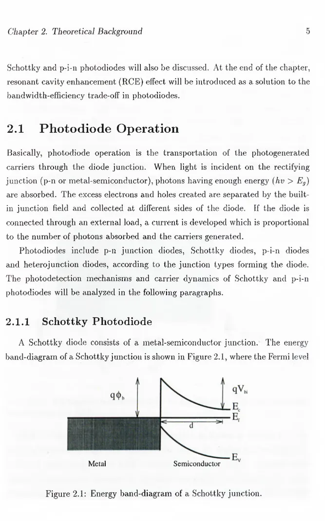
A Schottky diode consists of a metal-semiconductor junction. The energy band-diagram of a Schottky junction is shown in Figure 2.1, where the Fermi level
Chapter 2. Theoretical Background
5
Metal
Semiconductor
pinning at the interface can be seen. The difference between the work functions (difference between vacuum level and Fermi level) of metal and semiconductor is defined as the contact potential, q<f>b, and acts as a potential barrier for the charged carriers. This potential barrier forms a depletion region with a total voltage drop of Vbi (built-in potential) across this region. The resulting device is a Schottky diode, which acts as a voltage rectifier.^® Schottky photodiodes are excellent for detection of UV and visible radiation and are the fastest semiconductor photodetectors available. However, these diodes show poor efficiency performance, due to thin absorption regions and the highly absorbing metal layer.
Chapter 2. Theoretical Background
6
Ohmic
Schottky
Figure 2.2: Photogenerated carriers drift to the Schottky and ohmic contacts under the electric field.
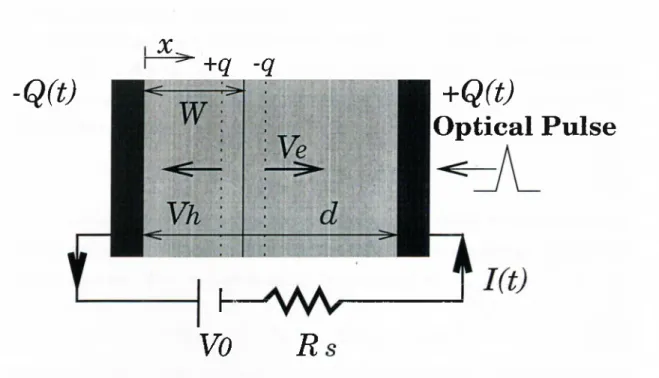
Such a diode can be used for photodetection as shown in Figure 2.2. By applying sufficiently high bias voltages, the whole n~ region can be depleted, so that a continuous electric field is created across this region. Photons with sufficient energies are absorbed in the depletion region and electron-hole pairs are generated. The generated carriers are swept away by the electric field. While
Chapter 2. Theoretical Background X .
-Q(t)
rq -q
+ Q ( t )Optical Pulse
I---Vo R
Figure 2.3: The carriers generated at a depth W induces an output current during their transport across the depletion region.
electrons move to the n'^ doped semiconductor, holes are swept towards the Schottky metal and an output current is observed at the external circuit.
The carrier dynamics of a Schottky photodiode can be described and calculated^'* by using a simple diagram shown in Figure 2.3. The depletion region can be described as a parallel plate capacitor, C = ek jd where e is the dielectric constant of semiconductor, A is the diode area and d is the depletion width. At stecidy state, the voltage bias on the capacitor is Vo, which results in a steady state total charge of Qo = CVq across the capacitor.
The position dependent electric field across the depletion region, E[x) has the following relation with the bias voltage:
Vo E{x)dx (
2
.1
)Jo
Let’s assume that, at i = 0, a narrow optical pulse generates carriers with a total charge of q, at a depth W from the Schottky surface. This will generate traveling
positive and negative sheet charges with sheet diarge densities p and —p, where
p = q/A. The positively charged sheet corresponds to the holes moving at the hole drift velocity, Vh and the negatively charged sheet denotes the electrons with electron drift velocity, Ve- As a result, an additional electric field is formed between the sheets.
Chapter 2. Theoretical Background
8
■t/cr -- -- .
e Ae (
2
.2
)The direction of this field is opposite to the depletion region electric field E{x),
which results in a voltage drop across the capacitor as the charge moves away from each other. This voltage drop can be expressed as
14,(t) = I Eadx = Ea[x^{t) - .r/i(t)] (2.3) where Xgt and Xht are the time dependent coordinates of the negative and positively charged sheets. These time dependent coordinates can be expressed as,
Xe{t) = W-\-Vet for 0 < i < te (2-4)
Xh{t) = W — Vht for 0 < f < th (2.5) where the electron transit time, /g = {d—W)lve^ and hole transit time, th = W/vh
are defined as time durations required for each carrier to complete its transport. Assuming th > tg and using Equation 2.18 we can express the time dependent voltage drop as.
Vc{t) =
-^{Vg + Vh)t for 0 < t <t g jpVht for t g < t < th
Inserting this equation into the following two equations.
(2.6)
(2.7)
Chapter 2. Theoretical Background
The induced output current, Cut can be written as
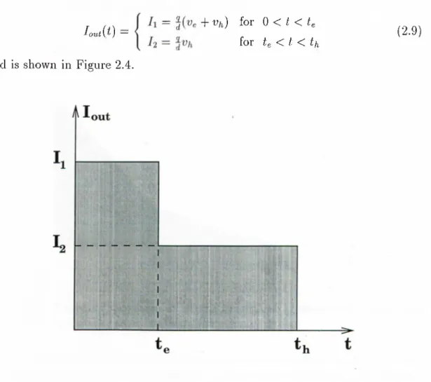
Cutii'') —
cind is shown in Figure 2.4.
= + Vh) for 0 < t < te
for tg < t < th (2.9)
Figure 2.4: Time-dependence waveform of the induced current.
The total charge under the curve equals to confirming the charge conservation of the system. An amount of charge generates a current such that the same amount of charge accumulates on the capacitor. Once all the carriers reach to the parallel plates, they recombine with these excess charge and steady state is reached.
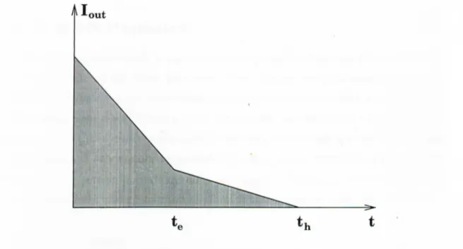
The analysis above was for a charge generation at x = W. If we integrate over entire depletion region, d, we obtain the output current waveform as shown in Figure 2.5. Here Vg > Vh is assumed, which is the case for most of semiconductors. Also a uniform density of photogenerated carriers, e.g. constant
Chapter 2. Theoretical Background
10
optical power across the depletion region is assumed, which is a valid assumption for semiconductors with small absorption coefficients.
Figure 2.5: Expected waveform of output current of a photodiode where hole drift velocity is smaller than electron drift velocity.
The output current is proportional to the number of carriers that continue their transport. At t = 0, the number of carriers that induce the output current is maximum, so that lotu displays its maximum at that time. But as the carriers closest to the metal and the other end of the depletion region complete their transport, the number of carriers continuing their transport decreases at a linear rate. At t = te, the last electrons drifting from x = 0 to x = d have completed their travel, while there are still traveling holes. Holes generated at x — d
complete their transport the latest, at i = d/vh. The slowering effect of holes is seen as a tail in the output current waveform. This is a major problem of photodiodes
as
high-speed operation is concerned. One can get rid of this problem by using heterostructures, i.e. using different materials for absorption region andintermediate regions. All layers but the absorption layer will
betransparent
for the spectrum of interest, so that all electron-hole pairs are generated only in thisChapter 2. Theoretical Background
11
region. By adjusting the placement of the active region, the response time of the diode can be minimized by equalizing the hole transit time to the electron transit time, so that no tail is observed at the output waveform.
2.1.2
P -I-N Photodiode
A p-n junction photodiode is a p-n junction operating at reverse bias mode. The reverse current of the diode increases when carriers are photogenerated in the depletion region. A p-i-n photodiode is a p-n junction diode with an intrinsic (i) layer between the p and n layers, p-i-n photodiodes are suitable for high-efficiency operation. If the intrinsic region is fully depleted with a high reverse bias voltage, photogenerated carriers are separated and swept to the terminals of the device: holes drift to p-region, electrons drift to n-region. Figure 2.6 shows the typical structure and the energy-band diagram of a homojunction p-i-n photodiode.
Incident
Figure 2.6: Photodiode structure and energy band-diagram of a homojunction p-i-n photodiode.
Chapter 2. Theoretical Background
12
Classical (homojunction) p-i-n photodiodes lack from high-speed operation since there is a diffusion component in the output current. The carriers which are photogenerated within the p and n layers can only contribute to the photocurrent by diffusing into the intrinsic layer. Once they reach the i layer, they are swept by the high electric field. Since these carriers are diffusing instead of drifting within the doped layers, these diodes demonstrate much slower operation speeds than Schottky photodiodes. To overcome this handicap, heterojunction p-i-n photodiodes can be utilized, where p and n layers have a wider bandgap than i layer so that no photogeneration occurs in these layers. So there is no diffusion current contributing to the output current. Hence with heteroj unction p-i-n photodiodes high efficiency can be achieved with high operation speeds.
The carrier transportation mechanism in a p-i-n photodiode is very similar to the Schottky photodiode. Instead of a. metal, there is a doped layer. The current-voltage characteristics are also very similar. Similar lout waveforms are expected from a heteroj unction p-i-n photodiode, whereas for a homo junction p-i-n photodiode a long tail is expected due to the diffusion current.
2.2
D io d e C haracteristics
Photodiodes have three main characteristics: I-V (current-voltage), quantum efficiency, and bandwidth (operation speed). Performance of a photodiode is measured with these three characterizations.
2.2.1 Current-Voltage
Photodiodes obey the well-known current-voltage relation for diodes.
(
2
.
10
)
Low dark current and high breakdown voltage are two indicators of diode junction quality. Low dark current means higher sensitivity. It is the current flowing through the diode under reverse bias and without illumination. The photodiodeChcipter 2. Theoretical Background
13
operates in the avalanche breakdown region when sufficiently high reverse bias is applied. This reverse bias voltage value corresponds to the breakdown voltage and determines the limit of reverse bias voltage that can be applied for photodiode operation. After this value, gain and multiplication mechanisms begin to effect the diode operation.^'^
2.2.2
Quantum Efficiency
Quantum efficiency of a photodiode, ?/, is defined as the probability that a single photon incident on the photodiode will create an electron-hole pair that contributes to the output current, i.e. it is the ratio of the number of detected electrons to the number of incident photons. For classical photodiodes the expression for quantum efficiency is
, = (1 _ n ) ( l - e - “‘ )
(
2
.
11
)
where R is the front surface reflectivity, a is the power absorption coefficient cind d is the thickness of the absorbing semiconductor layer. The first term represents the transmitted optical power and the second term denotes the portion of optical power absorbed during the single pass through the absorbing layer. So to maximize the quantum efficiency, one should minimize the detector surface reflectivity, R and maximize the single pass absorption, ad. R can be minimized for a specific spectral range using anti-reflection coatings. Single pass absorption can be simply increased by increasing d. So, it is not a difficult task to achieve near-unity quantum efficiencies.
2.2.3
Bandwidth
Another important device characteristic is the operation speed (bandwidth) of the photodiode. As discussed previously, the response time is mainly limited by the transit times of the photogenerated carriers. The other factors are the RC time constant of the photodiode circuit and diffusion of carriers generated in the undepleted regions. Schottky and heterojunction photodiode designs solve
Chapter 2. Theoretical Background
14
the carrier diffusion problem. Transit times can be reduced by decreasing the depletion region width, cl. However if d is decreased, the capacitance increases and RC time constant becomes the main bandwidth limitation. The transit time and capacitance limited .3 dB bandwidths are respectively expressed as
fi r = 0 .4 5
-fn c = cl
(
2
.12
)(2.13)
2rReA
where d is the depletion width, v is the carrier drift velocity, R is the total resistance, A is the device area and e is the permittivity of the semiconductor. For a given A and R, there exists an optimum d value. By reducing the active layer thickness one should be able to achieve high bandwidths as long as the capacitance is concuri'ently decreased by reducing the device size. So assuming no capacitance limitation, bandwidth of the photodetector is inversely proportional to cl.
2.2.4
Bandwidth-Efficiency Trade-ofF
It is desirable to achieve both high speed and high quantum efficiency with a single photodetector. However cis discussed above, bandwidth and efficiency have inverse dependencies on active layer thickness, cl. Near unity quantum efficiencies and veiy large bandwidths can be realized with very thick and very thin absorption layers respectively. But for any c/, bandwidth-efficiency product remains almost constant. The bandwidth-efficiency product of a photodetector determines its overall performance. To combine high efficiency and high bandwidth, one needs to increase this product. Resonant cavity enhancement (RCE) effect offers a clever solution to increase the bandwidth-efficiency product of a photodiode.
Chcipter 2. Theoretical Background
15
2.3
R eson an t C avity E nh an cem en t
This effect is first proposed by Unlu et. al. in 1990^® and is applied to a broad range of photodetector types; Schottky,^^’^^ p-i-n^®’·^*^ and a.valanche'^^’^^ photodiodes. The basic idea is to place the photodiode inside a Fabry-Perot resonant microcavity, so that the optical field builds up at resonant wavelengths. Enhcincement of the optical field at resonant wavelengths allows us to use thinner absorbing layers, meaning that we can achieve higher bandwidths without sacrificing from quantum efficiency, leading to higher bandwidth- elficiency products. Such photodiodes are called resonant cavity enhanced (RCE) photodetectors and are promising candidates for high performance detection in optoelecti’onic integrated circuits (OEICs).
So what is the cost for this performance improvement? Eirstly, a complex epitaxial design is required. Therefore the MBE growth of an RCE photodiode wafer is much more difficult than a conventional detector. It needs a very controlled and sensitive epitaxial growth. Hence an RCE photodetector is much more expensive. Another main drawback is the wavelength selectivity introduced by the resonant cavity. Although we obtain high efficiencies at resonant wavelengths, quantum efficiency at off-resonance wavelengths is suppressed. Actually this feature may be seen as an advantage for applications which require wavelength selectivity, such as wavelength division multiplexing (W DM ) in optical communication systems.
2.3.1 RCE Photodiode Operation
Figure 2.7 shows the typical epitaxial structure of an RCE photodiode. The conventional photodiode with a thin absorbing region is placed inside a Fabry- Perot microcavity. The front and back mirrors are distributed Bragg reflectors (DBRs) which consist of quarter wavelength thick alternating layers of non- absorbing larger bandgap materials. The incident optical field bounces back and forth between the mirrors, so that the photons at resonance are recycled. Hereby the effective absorbing layer thickness is increased and high quantum efficiencies
Chapter 2. Theoretical Background
16
Incident Light Active Layer D B R l (Ri) • · ·Figure 2.7: Typical RCE photodiode structure. Front and back mirrors are DBRs designed for operation wavelength.
can be obtained. Assuming no RC limitation (since a small d is used), the carrier transit times decreases, so that faster operation becomes possible. Hence, with this structure both high speed and high quantum efhciency photodetection can be achieved.
The quantum efficiency expression for an RCE photodiode with lossless cavity and mirror layers is derived as,^^
(1 + R 2e-“ '^)
1 — y/RiR2^ °“^cos{2kL + V’l T V’2) T R iR 2^
(2.14) where R\ and R2 are the front and back mirror reflectivities respectively, a is the cibsorption coefficient of the absorbing layer, d is the active layer thickness, k
is the propagation constant, L is the cavity length and 0i and ■02 are the phase shifts introduced by the front and back mirrors respectively. One can deduce very important design criteria from Equation 2.14.
Chapter 2. Theoretical Background
17
2.3.2
Design Parameters
Comparing the quantum efficiency formulations of a conventional and an RCE photodiode (Equcvtion 2.11 and 2.14), the enhancement factor comes out as,
Enhancement = (1 + R 2 e ~ n (2.15)
1 - y/R[R^e~°”^cos{2kL + V’l + 'ip2) +
When R2 = 0, this term becomes unity. No RCE effect is observed in this case, which is equivalent to the conventional detector. Therefore, the most crtitical design parameter in an RCE photodetector design is the back mirror reflectivity,
R2· For near unity quantum efficiency operation, a near unity reflectance back mirror is needed. DBRs are widely used for this purpose. Depending on the materials used, mirrors with reflectivities for desired spectral ranges bej^ond 99% can be designed. Front mirror reflectivity, Ri and single pass absorption, ad
are the other important design parameters. RCE effect is best observed for small single pass absorptions, with small d and moderate a values. Ri can be optimized with respect to R\ and ad, for maximum peak efficiency at resonance wavelength.
The enhancement term also indicates a periodic variation of quantum efficiency due to the term cos{2^L + V’l + V’2)· h is enhanced periodically at resonant wavelengths which occur when 2/dL + '0i + ¡/>2 = 2mTr{m = 1 ,2 ,3 ,...). This term introduces the wavelength selectivity of the RCE photodetector.
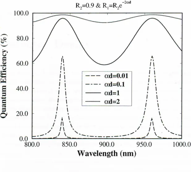
We analyzed the quantum efficiency siiectrum of an RCE photodiode as a function of R2, Ri and ad and plotted the simulation results in Figure 2.8, 2.9 and 2.10. The simulations are done for an idealized RCE photodiode with O.hpm
cavity length, lossless cavity and wavelength independent mirror reflectivities. In Figure 2.8, we simulated the effect of back (bottom ) mirror reflectivity, R2
on the quantum efficiency spectrum, for ad = 0.1 and Ri = 0.6. The results show a strong dependence between R2 and t]. The flat response corresponds to the conventional photodiode with no bottom mirror {R2 — 0). The quantum efficiency is below 5%, which the single pass absorption, t] is enhanced at the resonant wavelengths as R2 is increased. A maximum quantum efficiency of 85% is achieved with a nearly perfect (i?2 = 0.99) back mirror.
Chapter 2. Theoretical Background
18
ad=0.1 & Rj=0.6
Wavelength (nm)
Figure 2.8: Quantum efficiency spectrum of an RCE photodiode as a function of bottom mirror reflectivity, R2.
The quantum efficiency dependence on front (top) mirror reflectivity, Ri
is shown in Figure 2.9. For a given ad and R2, there exists an optimum Ri
value, which can be derived from Equation 15. By taking the derivative of this expression with respect to Ri and equating to 0, the optimum Ri value is found as.
Ri — R2^-2ad (2.16)
which corresponds to the perfect phase matching condition. We simulated the RCE structure for ad = 0.1 and R2 = 0.9. As we increased R\ upto the matching
Chapter 2. Theoretical Background
19
ad=0.1 & R2=0.9
Wavelength (nm)
Figure 2.9: Qucintum efficiency spectrum of an RCE photodiode as a function of front mirror reflectivity,
value, Ri — 0.74, the peak t] values improved. By further increasing Ri we deviate from the matching condition, so that the cpiantum efficiency is decreased. Full width at half-maximum (FW HM) gets narrower as Ri is increased.
The third design parameter, ad, is another important optimization term in RCE photodetection. Four different ad values are simulated with R2 = 0.9 and
Ri = in Figure 2.10. Although r) is increased at resonant wavelengths for higher ad values, RCE effect nearly disappears for ad > 2, i.e. a flat, near unity quantum efficiency is observed for ad = .5. In such designs almost all optical power is absorbed during the single pass, so that a little portion of the
Chapter 2. Theoretical Background
20
optical field is recycled. Therefore the wavelength selectivity gets weaker as ad
is increased. FWHM of the peaks are proportional to ad.
R 2=0.9 & R j—R2C -2a d
Wavelength (nm)
Figure 2.10: Quantum efficiency spectrum of an RCE photodiode as a function of ad.
Chapter 3
Detector Design
In the previous chapter, we briefly reviewed the RCE-detection scheme as a possible candidate for high-performance detection. However, the realization of such a theoretical model requires substantial amount of theoretical and experimental effort. Benefiting from the previous research work done in this area, we first chose the spectrum of interest and the material system to work on. We then optimized the detector performance by theoretical simulations, and finally ordered the designed structures for MBE-growth. In this chapter, we will briefly introduce the material systems that are or can be used for an RCE photodetector structure. The advantages and disadvantages of each material system will be discussed. Afterwards, the simulation method - Scattering Matrix Method - that we used to simulate and optimize the photodiode performance will be reviewed. We will then explain the optimized Schottky and p-i-n photodiode designs. The reflectivity measurements of the MBE-grown samples will be compared with our theoretical simulations. Finally, the wavelength tuning of the as-grown samples using a recess etch will be described.
3.1
M a te ria l S ystem s for R C E -P h o to d e te c to rs
Optical frequencies cover a significant portion of the electromagnetic spectrum, starting from the ultra-violet (UV) and extending to the far infrared. Each
Chapter 3. Detector Design 2 2
spectrum range has its specific applications; UV for military applications, visible and near infrared for optical fiber communication, jnid- and far-infrared for sensing and medical applications. There is an enormous commercial investment on optical fiber communication which relies on optoelectronic components working at optical communication window wavelengths. These wavelengths are 0.85/im, l.Spm and 1.55^¿m, denoting the first, .second and third communiciition windows for optical fibers respectively. While the 0.85/im window was the first one used in fiber-optic communicatiop, the transmission medium(glass fiber) has the largest attenuation with respect to the other two windows. At A = 1.3pm, the fiber demonstrates near-zero dispersion by cancelling the material and waveguide dispersion at this wavelength but shows larger attenuation than the third communication wavelength, A = 1.55pm. At A = 1.55pm, the optical signals traveling through the fiber medium see minimum attenuation. This results in a lesser number of repeaters, and hence a smaller cost for the signal transmitted over the same distance.
The performance of an optical communication system is measured with its bandwidth-cost product. To increase this product there is demand for high- performance system components, including photodetectors, operating at these optical fiber communication wavelengths. We know that RCE photodetectors offer this high-performance along with high quantum efficiencies. From an experimental point of view, one can summarize the features of a proper material
tern for RCE-detection as the following:
• Lattice matching between the materials
• Low-loss cavity (non-absorbing cavity and mirror materials) • High-reflectance bottom mirror (DBR)^'*
• Moderate active layer absorption coefficient
Fortunately several material systems fulfill most or all of these requirements in different optical communication w i n d o w s . L e t ’s have a brief look at the
Chapter 3. Detector Design
23
alternative material systems for RCE-detection and criticize them with respect to the requirements listed above:
1. A lG a A s /G a A s : The MBE growth of this material system is relatively easy, since there is an excellent lattice match between GaAs and AlAs. GaAs is used as the active layer which has moderate absorption coefficient and demonstrate good carrier transport characteristics. Also the relatively high refractive index contrast between GaAs and AlAs results in near unity reflectivity DBR mirrors. However the bandgap of GaAs lies around 0.87pm, meaning that we can operate only in the first optical communication wavelength, A = 0.85pm. Low-loss cavity formation is possible by using Alj,Gai_a;As cavity layers and AR.Ga.i_a;As/AlAs alternating layers for bottom DBR.
2. A lG a A s /G a A s /I n G a A s : This material system extends the operation wavelength of the above material system by incorporating Iiia^Gai-x-As active layer instead of GaAs. As the In concentration increases the bandgap of the active material decreases, so that detection at longer wavelengths become possible. But still one cannot go to the 2nd and 3rd optical communication windows with this material system, since it is very hard to grow In^Gai-.,; active layer on AfcGai-^As due to the lattice mismatch between these materials. Although Ino..53Gao.-)7As has the ability to absorb light at 1.3/im and 1.55pm, it should be grown on a substrate different than GaAs. High-performance RCE photodiodes operating around 900 nm have been demonstrated using this material systern^’^’"^'^
3. I n P /I n G a A s /I n A lA s : If InP is used as a substrate for Ino.53Gao.47As/Ino,52Alo.48As alloy system, excellent lattice matching and electrical properties with moderate absor])tion coefficient for RCE- detection at 1.3/i7n and l.55pm become possible. The main disadvantage of this material system is the low refractive index contrast between InGaAs and InAlAs which increases the number of periods required for a good bottom DBR. Even if this problem is solved by careful MBE growth.
Chapter 3. Detector Design
24
still one cannot form low-loss cavities using this material system since InGaAs layers forming the cavity and bottom mirror have absorption at the wavelengths of interest. To overcome this di'ciwback, transparent G aA s/A lA s bottom mirrors can be wafer-fused to the Fabry-Perot m i c r o c a v i t y . T h i s material system is one of the best candidates for RCE-detectors that can be used in fiber-optic communications.
4. Si/SiGe: The most important advantage of this material system is the integrability with the well-developed silicon-based electronics. Si/Sio.8Geo,2 combination is lattice matched up to a thickness of 0.1 pm, and this limit allows MBE growth of DBRs for A = 1.55pm using this material system.^® The main drawbacks are similar to the ones faced with InP/InGaAs/InAlAs material system: poor refractive index contrast leading to low performance bottom DBR and absorbing cavity and mirror layers make difficult to form low-loss cavities. Also, Si and Ge are indirect-bandgap materials, meaning smaller absorption coefficients and therefore reduced RCE-performance. However, successful RCE detectors are reported with this material system at shorter wavelengths around 700 nm.^^’“*“
5. Ternary and Quaternary Material Systems: In recent years with the enormous development in VCSELs (vertical cavity surface emitting lasers) new material systems are developed for optical communication wavelengths. The aim was to overcome the low index contrast and lossy cavity problems at 1.3pm and 1.55/im. Some examples which offer potential are InGaAsP/InP,'*^ AlGaAsSb/AlAsSb, AlGalnAs/AlAsSb.'*^ For shorter wavelength operation AlGaInP/GalnP, AlGaP/GaP, AlGaAs/Al-oxide are promising materials for high-performance optoelectronic applications including RCE-detection. Especially GaAs/Al-oxide DBRs offers excellent bottom mirrors with smaller number of periods.
Optical fiber communication systems operating at 1.3pm and 1.55pm are used for wide area networks (WANs), long-haul and sub-marine systems which connect cities, countries and continents. Then the question is: Is there still
Chapter 3. Detector Design
25
need for GaAs-basecl systems working at A = 0.85/¿m? The answer is yes, but not in long-distance communication. Systems working around the first optical communication window are widely employed in local area networks (LANs) where the attenuation in optical fiber becomes tolerable. AlGaAs/GaAs and AlGaAs/GaAs/InG aAs material systems are the best choices for this operation wavelength. Besides the excellent features we have discussed previously, its compatibility with GaAs fabrication technology and the existence of a developed fabrication process for GaAs-based photodetectors makes the AlGaAs/GaAs material system attractive for RCE-photodetection. Hence, our motivation in this work is to demonstrate high-performance RCE photodetectors working at the first optical communication wavelength using the AlGaAs/GaAs material system.
3 .2
D ev ice Sim ulation
A powerful simulcition technique is vital to make proper designs. Since our detector designs are rather complicated and difficult to grow -therefore expensive- , we should be able to analyze and optimize our designs well before ordering them for MBE-growth. An RCE photodetector structure consists of multilayer optical films, and therefore we need a simulation method by which we can analyze the optical field in such multilayer structures. Several simulation techniques, including the scattering matrix method (SMM), offer a systematic approach to analyze multilayer structures. We have used the S-matrix method in our simulations which was developed by Mutlu Gokkavas.'*'* This method provides a simple technique to calculate the exact field distribution within the cavity.
Of course simulations assume somewhat ideal conditions. When employing the S-matrix method to simulate our designs some assumptions are made. First of all, the incoming light is assumed to be a monochromatic plane- wave. Second, these plane-waves are assumed to reach the detector surface with normal incidence, so that reflections from all interfaces inside the cavity can be calculated using Fresnel’s coefficients. Another idealization is the perfect
Chcipter 3. Detector Design
26
interface assumption between different material layers. However, this is never the case in a real MBE-grown Scimple. Structures are assumed to have no defects and the diffraction of the optical field near the boundaries are omitted, i.e. the layers extend over the entire plane of nornicil incidence. So, propagating the optical field through multilayer structure becomes a one-dimensional problem which simplifies our calculations.
E
Port 1
► iPort 2
E
bl
Figure 3.1: Traveling waves entering and leaving an optical two port layer.
The S-matrix method we have used in our simulations is nothing but an analogy of transmission-line theory. Each layer in the multilayer stack corresponds to a two-port transmission line with a normalized characteristic impedance Z = 1/??., where = n/j + ini denotes the complex refractive index of the layer material, ur and nj represent the real and complex part of the refractive index respectively. Traveling waves are used in transmission-line theory to characterize the two-ports in terms of S-parameters. S-parameters of a two- port system represent the waves leaving the two-port in terms of the waves entering the two-port. These traveling waves are shown in Figure 3.1, where
Cheipter 3. Detector Design 27
E f 2 ^12 ^’21 E f 2
- ^ 1 2 ¿21 Eb i
the wave-equation is linear, using the superposition principle, one can write the output variables as a linear superposition of the input variables:
(3.1) where tij and r{j represent the field-transmission and field-reflection coefficients for waves traveling from port i to port j. The matrix corresponds to the S-matrix of this two-port element.
Using signal-flow graphs, one can derive the formulation for cascading S- matrices.^'^ Eliminating the waves traveling between the intermediate ports, we can obtain reflection and transmission coefficients of the entire multilayer stack. Optical multilayer structures can be thought as multi-port systems with 2 different kind of two-port elements:
• Sin gle Layer : Denoted with Stayer- Represents the propagation of light in a single layer without any interfaces. For a layer with thickness d, the corresponding ,5'/ayer-matrix is written as
Slayer —
çikd- fd
0
Akd-^d0
(3.2)where k = 27r?7./?/A and o: = 47rn//A are the j^ropagation ¿ind attenuation constants respectively, and A is the free-space wavelength of the incident light field. No reflections occur, therefore Vij = 0 . If a 0, then the propagating light waves will undergo a magnitude modification besides a phase shift due to propagation inside the medium.
• Interface : This kind of two-port element corresponds to a physical boundary between two different materials. Sinterface is totally determined by Fresnel’s reflection and transmission coefficients for normal incidence:
5.interface — 2 m n \ — ?i2 n i-\-U2 + ri2 r i2 -n \ 2H2 n i+ ri2 ni-fri2 J (3.3)
Chapter 3. Detector Design
28
where ?гх and П2 are the complex refractive indices of the two neighbor layers. Ideal interfaces have no thicknesses, therefore the field phasers don’t change. At limiting case, when ni = П2, Sinter face becomes equal to S'layer for d = 0.
S la y e r and S in t e r fa c e ai'c the building blocks of ОПГ Calculations. Using S la y e r 1
S in t e r f a c e and the rules for cascading S-matrices, S-parameters (transmission and
reflection coefficients) of any passive multilayer stack can be determined. The only data we need is the complex refractive index data of the materials used in the stack, which is well-documented for AlGaAs/GaAs material system.''*^
When we measure the reflectivity of a sample, we measure the power reflectivity, not the field-reflectivity. The same is valid for transmittivitjc Using the following formulas, field coefficients are converted to power coefficients:
= b o f (3.4)
(3.5) Calculation of absorption is another important calculation for optimizing the quantum efficiency of the design. With S-matrix approach, absorption in single/multi layers can be calculated using the following procedure. The optical power entering and leaving the absorbing layer(s) is calculated and differentiated so that the remaining amount is the power absorbed in the absorbing region. In other words, one should differentiate the power transmitted to the right side of the absorptive fcvyer(s) and the power transmitted to the left side of the absorptive layer(s). Hence, S-matrix method allows us to simulate the reflection, transmission and absorption spectrums of our optical multilayer design structures.
As stated earlier, it is desired to have a perfect bottom mirror for high- performance RCE-detection. Metals are known as good reflecting materials. However they are not perfect mirrors {R < 96%), and show variance along the spectrum. Another major disadvantage of metal mirrors is thcit they are strong absorbers at optical frequencies, so that low-loss cavities can’t be formed with
Chapter 3. Detector Design
29
Port 1
Port 2
Figure 3.2: Quarter wave stack as a two port.
these mirrors. Instead DBRs are used widely in optoelectronic applications. A DBR is a periodic stack with two alternating quarter-wave thick materials (Figure 3.2). uh and ul a.i'e the complex refriictive indices of the high-index and low-index material respectively. Ac is the design wavelength of the mirror. Applying the S- matrix method to this structure the peak power reflectivity at central wavelength comes out as
Rpeak —
n2NH „2N'l ^
n''H2N
+
^ 2N( (3-6)where N is the number of mirror-pairs in the stcick, nn and n/, are the complex refrcictive indices of the high-index and low-index material respectively. For a constant period number N, the critical design parameter is the refractive index contrast between the mirror materials, A?i = np - n i. With higher contrast mirror layers we can achieve higher reflectivities for the same N. GaAs/AlAs DBR offers the maximum index-contrast for the mciterial system used, but is not suitable for design wavelengths shorter than 0.87pm. Therefore for a DBR design at 0.84^im, it is preferable to use Alo.2Gao.8As and AlAs as mirror materials. The
Chapter 3. Detector Design
30
bandgap of Alo.2Gao.8As lies around 0.75fim. so that we can get rid of absorption in mirror layers. Figure 3.3 shows the simulation of the reflectivity spectrum of a Alo.2Gao.8A s/A lA s DBR as a function of N, the number of periods of DBR.
Wavelength (nm)
Figure 3.3: Reflectivity spectrum of Alo.2Gao.8A s/A lA s DBR for N=10, 15 and 20. Design wavelength is 840 nm.
As N increases, the reflectivity increases and reaches 99% for N — 20. So, in order to have a significant RCE effect, a bottom DBR with N ~ 20 is needed. It is preferable to have a 30 or 40 period bottom DBR, but this increases the cost of the MBE growth. In the following sections the RCE-photodetector designs that we worked on will be introduced: RCE Schottky and RCE p-i-n photodetector designs.
Chapter 3. Detector Design
31
3 .3
S ch ottk y D esign
As discussed in Chapter 2, Schottky photodiodes can achieve very high operation bandwidths since they are majority carrier devices. But these devices lack from poor quantum efficiencies. The design shown in Figure 3.4 is made to overcome this handicap without sacrificing from operation speed.
3.3.1 Design and Optimization
The design wavelength of the RCE-Schottky photodiode is 0.84/im so that it can operate within the 1st optical communication window, and can be utilized in LANs. GaAs has a moderate absorption coefficient (or ~ around the operation wavelength and is ideal as active region of the detector. The active layer thickness is 1 2 0 nm, which corresponds to about a half-wavelength thickness. Why not thinner or thicker? The answer of this question lies in the standing wave effect (SW E), an effect introduced by the cavity.
The forward and backward traveling waves in the cavit}^ form a standing wave pattern at steady state. The period of this standing wave pattern is equal to A /2. So for a A/2-thick active layer, the total optical power falling on the active region will be independent of the position of the active layer. If we make the active layer thinner, there is always a risk to coincide the active layer with a node of the standing wave which can be caused by growth variations. The quantum efficiency then can decrease dramatically. Of course, it is much better to use a thinner active region that coincides with a maximum of the standing wave pattern. This will improve the performance of the device, especially the bandwidth which will increase as the active layer gets shorter. But, this approach needs a very well controlled MBE growth and is much more sensitive to growth rate fluctuations. Therefore, it is safer to have a an active layer with A/ 2 thickness. Thicker active layers can also be used, at the expense of a decrease in the speed performance of the diode.
In order to have a low-loss cavity, Alo.15Gao.85As and Alo.2Gao.8As are used for intermediate cavity materials. Semi-insulating GaAs is used as the growth
Chapter 3. Detector Design
32
80 nm ' . SOnm ÔràâedloiilâlMf N * doped N*]'-êdÿea . -i 160 nm A1 ^ gAs N " doped400 nm Alg íA® N ^ doped
230 nm undoped
1 19 Pairs of 1
A1 g 8^® ^ AlAs
Distributed Bragg Reflector
i > rr lA"» í'-.¿
Figure 3.4: Epitaxial design of RCE Schottky photodetector.
substrate. Bottom mirror consists of a 18.5 period A lAs/A lo,2Gao.8As Bragg mirror designed at 840 nm. The 230 nm thick undoped Alo.2Gao.8As layer on top of the bottom DBR is the mesa isolation region of our diodes. Then comes the n'^
region, which is called as the ohmic layer. Ohmic contacts of the photodiodes are made within this 400 nm thick layer. This is followed by a 160 nm thick n~ buffer layer. On each side of the active layer, graded interfaces are employed. Sharp interfaces, i.e. interfaces without graded regions, cause carrier trapping problems near the interface. To get rid of this performance reduction, smooth interfaces are preferred in heterojunction devices. In our design, two graded interface regions are used to increase the detector performance. The graded regions are 30 nm thick and n~ doped. The top layer of the cavity is a 80 nm thick n~ doped
A lo .15G ao .8 5As layer. By etching this layer, one can tune/shift the resonance wavelength.