686 Vol. 45, No. 3 / 1 February 2020 / Optics Letters Letter
Bismuth plasmonics for extraordinary light
absorption in deep sub-wavelength geometries
Imre Ozbay,
1,* Amir Ghobadi,
2,3Bayram Butun,
2AND
Gonul Turhan-Sayan
1,41Department of Electrical and Electronics Engineering, Middle East Technical University, Ankara 06800, Turkey 2NANOTAM-Nanotechnology Research Center, Bilkent University, 06800 Ankara, Turkey
3Department of Electrical and Electronics Engineering, Bilkent University, 06800 Ankara, Turkey 4e-mail: [email protected]
*Corresponding author: [email protected]
Received 15 October 2019; revised 5 November 2019; accepted 6 November 2019; posted 7 November 2019 (Doc. ID 379670); published 30 January 2020
In this Letter, we demonstrate an ultra-broadband meta-material absorber of unrivaled bandwidth (BW) using extraordinary optical response of bismuth (Bi), which is the material selected through our novel analysis. Based on our theoretical model, we investigate the maximum metal– insulator–metal (MIM) cavity BW, achievable by any metal with known n-k data. We show that an ideal metal in such structures should have a positive real permittivity part in the near-infrared (NIR) regime. Contrary to noble and lossy metals utilized by most research groups in the field, this requirement is satisfied only by Bi, whose data greatly adhere to the ideal material properties predicted by our analysis. A Bi nanodisc-based MIM resonator with an absorption above 0.9 in an ultra-broadband range of 800 nm–2390 nm is designed, fabricated, and characterized. To the best of our knowledge, this is the broadest absorption BW reported for a MIM cavity in the NIR with its upper-to-lower absorption edge ratio exceeding best contenders by more than 150%. According to the findings in this Letter, the use of proper materials and dimensions will lead to realization of deep sub-wavelength efficient optical devices. © 2020 Optical Society of America
https://doi.org/10.1364/OL.45.000686
In recent years, the concept of plasmonics and metamaterials-based perfect light absorbers (MPAs) has attracted much attention due to their wide range of applications in photo-voltaics [1,2], thermal photovoltaics [3,4], photodetectors [5,6], photochemistry [7,8], solar vapor generation [9], imaging [10–12], sensing [13–15], and spectroscopy [16]. Near-unity harvesting of solar irradiation in sub-wavelength geometries, through strong light–matter interaction, can be realized using these MPAs. Metals, with their lossy nature in the whole electro-magnetic (EM) spectrum, are the most frequently utilized materials in the MPA design. These ultrathin metal-based MPAs can operate in narrow or broad frequency ranges [17–23]. The narrowband perfect absorbers have potential applications in sensing and filtering, while the broad ones are used in solar vapor generation, photochemistry, and photodetection.
Recently, different materials and design configurations have been proposed to enhance the light absorption bandwidth (BW). The most commonly utilized structure is based on the metal–insulator–metal (MIM) cavity [24–28]. The use of multi-dimensional resonant units and lossy top metals, and adding broadband antireflective coating on top of the MIM design, are some of these ideas [29–34]. However, due to the large negative real part of permittivity (εreal) of metals in the near-infrared (NIR) region, the absorption in these MIM cav-ities is limited to the visible regime [35]. Dinget al. proposed a tightly packed titanium-based nanodisc design to achieve perfect light absorption from 900 to 1850 nm [36]. It should be noted that the common strategies for the design of NIR MPA are based on using multiple metal–insulator pairs and nanos-tructured scaffolds [37,38]. However, these configurations are bulky, and they suffer from complex fabrication routes. In recent years, bismuth (Bi) was found to show extraordinary optical response. Similar to low-loss plasmonic metals, Bi has a small negativeεrealin the visible range. However, in the NIR regime, it acts as a lossy dielectric with a positiveεreal [39,40]. The deep sub-wavelength Bi plasmonics were already unveiled in ultraviolet, visible, and NIR regimes [41,42]. Very recently, a deep sub-wavelength (subλ/100) nanocavity design has been proposed to achieve perfect narrowband light absorption in the mid-to-far infrared range [43].
Here, we reveal an extraordinary absorption response from the Bi-based MPA. An ultra-broadband, polarization insensi-tive, and almost omnidirectional NIR perfect absorber will be demonstrated using Bi nanodiscs in an MIM configuration. Based on the transfer matrix method (TMM) modeling estima-tions, extraordinary response of Bi follows the data of an ideal MIM perfect absorber. The proposed Bi-based MIM nanocav-ity is designed, fabricated, and characterized. According to the measurement results, the Bi-based MIM cavity can provide above 0.9 the absorption from 700 to 2390 nm in a cavity thick-nesses in the order ofλ/10. To the best of our knowledge, this absorption BW is the largest compared to all previously reported MIM-based perfect absorbers. Furthermore, this wavelength range, the short-wave infrared (SWIR), is especially useful for thermal imaging applications, and MIM-based broadband 0146-9592/20/030686-04 Journal © 2020 Optical Society of America
Letter Vol. 45, No. 3 / 1 February 2020 /Optics Letters 687
Fig. 1. (a) Real and (b) imaginary parts of permittivity for different metals. The ideal absorption circles for three different top-material thicknesses ofDM=5 nm, 15 nm, and 30 nm at wavelength values of (c) λ = 1 µm, (d) 2 µm, and (e) 3 µm. (Color bar denotes the reflection amount.)
absorbers have previously been unable to conquer this regime completely (for reasons that we will reveal shortly). Contrary to mainstream semiconductor photodetector technologies such as InGaAs or InP [44,45], which can only cover a portion of the SWIR band and require low temperatures and complex fabrication routines, the findings of this Letter point to the possibility of the complete coverage of the SWIR band with an uncooled device at a significantly reduced price. As already stated, Bi shows an extraordinary optical response. Figures1(a)
and1(b)reveal the real (εreal) and imaginary (εimaginary) parts of permittivity for some common metals. The permittivity data for Bi have been extracted experimentally, and for the others, the Palik’s data [46] is used. According to this figure, theεrealpart gets a near exponential profile toward large negative values for most metals. However, a different story is true for Bi. In the vis-ible range,εrealstays in small negative values, while it gradually increases toward positive values in longer wavelengths. In other words, Bi acts simultaneously as a plasmonic metal in shorterλ values and a lossy dielectric in the longer ranges.
A theoretical model based on the TMM is developed to find the ideal material for perfect absorption in a planar MIM cavity, as explained in our previous works [35,47,48]. The overall reflection from the design is found using TMM. The model involves three layers: back-metal, dielectric, and top-metal layer. Our studies show that the dominant contribution to overall BW is due to the material choice of the thin top-metal layer; dielectrics usually have unsophisticated frequency response characteristics, and the back-metal material choice has little effect on overall response as long as it is reflecting. In other words, the search for ideal top metal is the most important part
of the search for the ideal device for a given application. To find the ideal top metal, we make no assumptions for the top metal, and instead, we impose the 0.9 absorption for the whole MIM device and solve the TMM equations that yield the “ideal” metal we are looking for. Compared to the finite-difference time-domain (FDTD) method, this enables us to solve thousands of configurations within minutes. In our unique representation, we draw circles that represent the solution domain of the ideal metals for a given configuration of fixed wavelength and fixed dimensions. Materials within this circular domain have a reflec-tion below 0.1 (absorpreflec-tion above 0.9), and thus these can be considered ideal metals for the given configuration. Circles are extracted for three wavelength values ofλ = 1 µm, 2 µm, and 3 µm. As we can see, for some configurations aroundλ = 1 µm, many metals can be utilized as they all fall in the solution domain; however, forλ ≥ 2 µm, the circles generally require positive real permittivity, yet almost every metal has a negative real part of permittivity. For this reason, the 700–3000 nm band has never been successfully covered with MIM-based absorbers with conventional metals. However, Bi has a positive real part of permittivity, and therefore, it can take the role of the ideal metal. As can be seen in the panels, Bi outperforms any other metal on the market since it falls inside (or near) a circle for all wave-lengths of consideration. Although the findings of this model are valid for a planar design, based on the effective medium theory, a nano unit metal resonator can be roughly treated as an effective medium with an effective permittivity between those of air and metal. This principle can be used to design a top layer that has an effective index between air and Bi, thus providing further flexibility for device optimization. In the next section, it will be demonstrated that ultra-broadband perfect absorption can be acquired, using a Bi-nanodiscs-based MIM cavity.
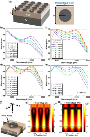
To obtain an optimal device with maximum absorption BW of the design, numerical simulations are conducted (Lumerical FDTD Solutions) [49]. Figure2(a)depicts the proposed MIM cavity. The optical performance of the cavity can be optimized by studying four main geometrical dimensions: 1) periodicity (P ), 2) spacer thickness (DI), 3) disc height (DM), and 4) disc
radius (R). The spacer layer is Al2O3, top discs are Bi, and the bottom layer is chromium (Cr). It should be noted that the theo-retical TMM and numerical simulation results were extracted using the Cr mirror. This is due to the fabrication considerations as, based on our experiences, Al2O3 has a better surface mor-phology and adhesion on Cr substrate. Moreover, Cr is rather lossy compared to other metals, and this can consequently sub-stantiate the absorption BW of the design. The experimentally extracted Cr permittivity data have been already reported in our previous work [48]. The unit cell shown in Fig.2(a)is excited with a plane wave spanning from 700 to 3000 nm in desired polarization and incidence angles.
The aim of the optimization was to obtain an ultra-wide BW that shows little sensitivity to fabrication discrepancies; there-fore, instead of an automated method, we used a semi-manual optimization scheme. As can be seen from the results, any vari-ance from the optimal device dimension (DI,DM,P , and R)
does not change our BW more than 2% within our design and fabrication. We found the optimal and stable dimensional region forDI,DM,P , and R as 145 nm, 25 nm, 600 nm, and
220 nm, respectively. As plotted in Fig.2(b), when the perio-dicity increases, whileDI,DM, andR are respectively fixed at
688 Vol. 45, No. 3 / 1 February 2020 /Optics Letters Letter
Fig. 2. (a) Schematic representation of the MIM nanocavity com-prising Cr−Al2O3−Bi layers. The inset shows the top view of the unit
cell. The absorption spectra for different sweeps on (b) periodicity (P ), (c) insulator thickness (DI), (d) top-metal thickness (DM), and (e) the radius of the nanodiscs (R). (f ) Schematic representation of the
view plane in the MIM cavity design. The H-field distributions in the resonance peak spectral positions of (g) 960 nm and (h) 2060 nm.
MIM cavity is diminished for longer wavelengths. This is in line with previous reports that a tightly packed nanodisc design can provide a strong light absorption in an ultra-broadband regime [35]. Ultra-broadband designs with 400 nm < P < 600 nm were theoretically evaluated; however, taking the fabrication complexities into account [in which smaller pitch length can be challenging in the electron beam lithography (EBL) processing], the P is chosen as 600 nm. In a MIM cavity, the spacer layer thickness defines the lower absorption edge. Therefore, in the next step,DMandR values are fixed at 20 and 200 nm, and DI
is swept from 100 to 160 nm. According to Fig.2(c), a spacer layer thickness in the range between 140 and 150 nm can set the absorption lower edge in 800 nm. Therefore,DIis fixed at
145 nm. A study of the impact of theDMdimension is shown in
Fig.2(d), which also shows that the absorption profile has two maxima. An increase in the disc height causes the longer wave-length peak to become stronger, while the shorter wavewave-length is gradually weakened. Finally, for fixedDI andDM values in
their above-mentioned optimal values, the effect of dimension R on absorption BW is studied. As the disc radius gets larger,
the second peak experiences a red shift. Based on the simulation results in Fig.2(e), at the optimalR = 220 nm, an absorption above 0.9 is accomplished from 800 to 2390 nm. This ultra-broadband BW mainly originates from extraordinary plasmonic response of Bi, together with Fabry–Perot (FP) modes and plasmonic modes.
To gain an insight on the origin of this absorption peak, the magnetic (H) field distributions have been plotted through the cavity length, as shown in Fig.2(f ). The H-filed distri-butions in λ = 960 nm (the spectral position of first peak) andλ = 2060 nm (the spectral position of second peak) have been plotted in Figs.2(g)and2(h). As plotted in Figs.2(g)and
2(h), in the first resonance, the magnetic field is mainly con-fined within the cavity and between two adjacent nanodiscs. However, it is mostly localized beneath the nanodisc unit for the second peak. Therefore, the shorter peak likely originates from diffractive coupling of the incident wave into propagating sur-face plasmons (PSPs) in the bottom metal–insulator intersur-face. However, the second peak (at 2060 nm) is due to the coupling of incident light into FP-standing waves within the cavity.
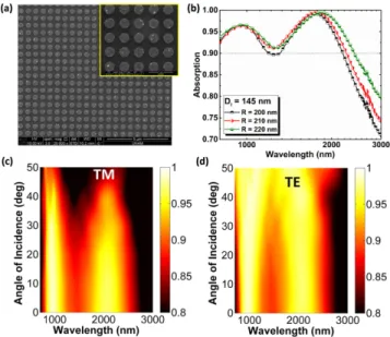
Finding the optimal geometries, the design is fabricated and optically characterized. The 150 nm Cr and 25 nm Bi layers are coated using a thermal evaporation tool (Vaksis Ar-Ge). An atomic layer deposition (Cambridge Nanotech Savannah S100) tool is used to coat the Al2O3spacer. To obtain Bi nanodiscs, the lift-off process was employed. For this purpose, electron beam lithography (RAITH E-Line Plus) was conducted on the sample using the 495 k poly(methyl methacrylate) (PMMA) resist with a thickness of 180 nm. For this process, 30 kV, e-beam spot size of 5 nm, and 350 pA beam current were used. The exposure dose was 3000 pC. The samples were developed by an methyl isobutyl ketone:isopropyl algohol (MIBK:IPA) (1:1) solution for 2 min, followed by an immersion in IPA for 30 sec. Figure 3(a) shows a top-view scanning electron microscopy (SEM) image of the sample. To make a comprehensive compari-son, the proposed MIM cavity was made for differentR values of 200, 210, and 220 nm. Figure3(b)shows the absorption spec-tra for these three cases. This optical characterization has been conducted using a Fourier-transform infrared (Bruker, Billerica, MA, USA, HYPERION 2000) system. The agreement between theory and experiment is superb with up to a 99.1% agreement between the experimental and theoretical spectrum. According to this panel, an absorption above 0.9 is attained from 800 nm to 2410 nm (2390 nm theoretically) for the case ofR = 220 nm. To the best of our knowledge, this is the broadest BW for a MIM-based cavity absorber. Moreover, the proposed design has a quite high angular absorption response. As depicted in Figs.3(c)and3(d), the strong absorption response of the design is retained in wide viewing angles for both transverse electric (TE) and transverse magnetic (TM) polarizations.
In summary, this work reveals the extraordinary capability of Bi to obtain perfect light absorption in the ultra-broadband wavelength range. It was found that the real part of permittivity for Bi has small negative values in visible and short wavelength NIR ranges. However, in moving toward longer wavelength values, these data follow a gradual increase toward larger positive amounts. According to our previous study, this is in good agree-ment with the permittivity data of an ideal unity absorber. With numerical simulations, the proposed MIM cavity is optimized in a way that the broadest absorption BW is achieved. This optimal configuration is fabricated and optically characterized.
Letter Vol. 45, No. 3 / 1 February 2020 /Optics Letters 689
Fig. 3. (a) Top-view SEM image of fabricated samples. (b) Absorption spectra obtained for the fabricated designs with different disc radii. Contour plots showing the change in the absorp-tion response of the MIM structure under different light incidence angles for (c) TM and (d) TE polarizations.
According to our findings, an absorption BW of 1610 nm is acquired in the MIM cavity thicknesses in the order ofλ/10. The simulation results also demonstrate that the proposed design has a high angular tolerance for both TE and TM polar-izations. The findings of this study can be applied to other optical metal-based designs. Finally, the strong index contrast between Bi and other metals can be employed for many other types of devices over the complete NIR range (1–30 µm) using proper topology and proper geometry.
Disclosures. The authors declare no conflicts of interest. REFERENCES
1. J. Grandidier, D. M. Callahan, J. N. Munday, and H. A. Atwater,Adv. Mater.23, 1272 (2011).
2. C. F. Guo, T. Sun, F. Cao, Q. Liu, and Z. Ren, Light Sci. Appl. 42, 1 (2014).
3. E. Rephaeli and S. Fan,Opt. Express17, 15145 (2009).
4. H. Wang, Q. Chen, L. Wen, S. Song, X. Hu, and G. Xu,Photon. Res.3, 329 (2015).
5. W. Li and J. Valentine,Nano Lett.14, 3510 (2014).
6. S. Song, Q. Chen, L. Jin, and F. Sun,Nanoscale5, 9615 (2013). 7. J. Lee, S. Mubeen, X. Ji, G. D. Stucky, and M. Moskovits,Nano Lett.
12, 5014 (2012).
8. T. G. U. Ghobadi, A. Ghobadi, E. Ozbay, and F. Karadas, Chem. Photo Chem. 2, 1 (2018).
9. L. Zhou, Y. Tan, D. Ji, B. Zhu, P. Zhang, J. Xu, Q. Gan, Z. Yu, and J. Zhu,Sci. Adv.2, e1501227 (2016).
10. K. Üstün and G. Turhan-Sayan,J. Opt. Soc. Am. B34, D86 (2017). 11. K. Üstün and G. Turhan-Sayan,J. Appl. Phys.120, 203101 (2016). 12. P. Bouchon, C. Koechlin, F. Pardo, R. Haïdar, and J.-L. Pelouard,Opt.
Lett.37, 1038 (2012).
13. S. Collin, G. Li, X. Chen, O. Li, and C. Shao, J. Phys. D 45, 205102 (2012).
14. N. Liu, M. Mesch, T. Weiss, M. Hentschel, and H. Giessen,Nano Lett.
10, 2342 (2010).
15. N. Liu, M. Mesch, T. Weiss, M. Hentschel, H. Giessen, and P. Institut,
Nano Lett.10, 2342 (2010).
16. K. Chen, R. Adato, and H. Altug,ACS Nano6, 7998 (2012). 17. X. Lu, R. Wan, and T. Zhang,Opt. Express23, 29842 (2015). 18. Y. Lin and W. Chen,Sci. Rep.8, 7150 (2018).
19. H. Peng, Y. Luo, X. Ying, Y. Pu, Y. Jiang, J. Xu, and Z. Liu,Appl. Opt.
55, 8833 (2016).
20. H. Deng, Z. Li, L. Stan, D. Rosenmann, and D. Czaplewski,Opt. Lett.
40, 2592 (2015).
21. K. Aydin, V. E. Ferry, R. M. Briggs, and H. A. Atwater,Nat. Commun.
2, 1 (2011).
22. Z. Liu and K. Aydin,Nano Lett.16, 3457 (2016).
23. A. Ghobadi, H. Hajian, M. C. Soydan, B. Butun, and E. Ozbay,Sci. Rep.9, 1 (2019).
24. A. Lefebvre, D. Costantini, I. Doyen, Q. Lévesque, E. Lorent, D. Jacolin, J.-J. Greffet, S. Boutami, and H. Benisty,Opt. Mater. Express
6, 2389 (2016).
25. M. Yan, J. Opt. 15, 250061 (2013).
26. G. Kenanakis, C. P. Mavidis, E. Vasilaki, N. Katsarakis, M. Kafesaki, E. N. Economou, and C. M. Soukoulis,Appl. Phys. A123, 77 (2017). 27. Z. Li, S. Butun, and K. Aydin,ACS Photon.2, 183 (2015).
28. G. Kajtár, M. Kafesaki, E. N. Economou, and C. M. Soukoulis,J. Phys. D49, 055104 (2016).
29. X. Liu, T. Starr, A. F. Starr, and W. J. Padilla,Phys. Rev. Lett.104, 207403 (2010).
30. H. Wang and L. Wang,Opt. Express21, 13311 (2013). 31. X. Ming and Q. Tan,Plasmonics12, 117 (2017).
32. M. Kenney, J. Grant, Y. D. Shah, I. Escorcia-carranza, M. Humphreys, and D. R. S. Cumming,ACS Photonics4, 2604 (2017).
33. X. Duan, S. Chen, W. Liu, H. Cheng, and Z. Li,J. Opt.16, 125107 (2014).
34. R. Mudachathi and T. Tanaka,Adv. Nat. Sci.: Nanosci. Nanotechnol.
9, 015010 (2018).
35. A. Ghobadi, H. Hajian, B. Butun, and E. Ozbay,ACS Photonics5, 4203 (2018).
36. F. Ding, J. Dai, Y. Chen, J. Zhu, Y. Jin, and S. I. Bozhevolnyi,Sci. Rep.
6, 39445 (2016).
37. Y. Cui, K. H. Fung, J. Xu, Y. Jin, S. He, and N. X. Fang,Nano Lett.12, 1443 (2012).
38. M. Lobet, M. Lard, M. Sarrazin, O. Deparis, and L. Henrard,Opt. Express22, 12678 (2014).
39. J. Toudert, R. Serna, I. Camps, J. Wojcik, P. Mascher, E. Rebollar, and T. A. Ezquerra,J. Phys. Chem. C121, 3511 (2017).
40. J. Toudert and R. Serna,Opt. Mater. Express7, 2299 (2017). 41. J. Toudert, R. Serna, and M. Jiménez De Castro,J. Phys. Chem. C
116, 20530 (2012).
42. J. M. McMahon, G. C. Schatz, and S. K. Gray,Phys. Chem. Chem. Phys.15, 5415 (2013).
43. J. Toudert, R. Serna, M. G. Pardo, N. Ramos, R. J. Peláez, and B. Maté,Opt. Express26, 34043 (2018).
44. M. H. Dolas and S. Kocaman,IEEE Electron Device Lett.38, 1692 (2017).
45. R. Fraenkel, E. Berkowicz, L. Bikov, R. Elishkov, A. Giladi, I. Hirsh, E. Ilan, C. Jakobson, P. Kondrashov, E. Louzon, I. Nevo, I. Pivnik, A. Tuito, and S. Vasserman,Proc. SPIE10177, 1017703 (2017). 46. E. D. Palik, Handbook of Optical Constants of Solids, Vol. 3
(Academic Press, 1998).
47. A. Ghobadi, H. Hajian, M. Gokbayrak, B. Butun, and E. Ozbay,
Nanophotonics8, 823 (2019).
48. A. Ghobadi, H. Hajian, A. R. Rashed, B. Butun, and E. Ozbay,Photon. Res.6, 168 (2018).
49. Lumerical Solution Inc., https://www.Lumerical.Com/Tcad-Products/Fdtd/.