MACROCRYSTALS OF SEMICONDUCTOR
NANOCRYSTALS FOR LIGHT EMITTING
DIODES
A THESIS
SUBMITTED TO THE DEPARTMENT OF ELECTRICAL AND ELECTRONICS ENGINEERING
AND THE GRADUATE SCHOOL OF ENGINEERING AND SCIENCE OF BILKENT UNIVERSITY
IN PARTIAL FULLFILMENT OF THE REQUIREMENTS FOR THE DEGREE OF
MASTER OF SCIENCE
By
Halil Akcalı
August 2013
I certify that I have read this thesis and that in my opinion it is fully adequate, in scope and in quality, as a thesis for the degree of Master of Science.
Assoc. Prof. Dr. Hilmi Volkan Demir (Supervisor)
I certify that I have read this thesis and that in my opinion it is fully adequate, in scope and in quality, as a thesis for the degree of Master of Science.
Prof. Dr. Ayhan Altıntaş
I certify that I have read this thesis and that in my opinion it is fully adequate, in scope and in quality, as a thesis for the degree of Master of Science.
Assoc. Prof. Dr. Hamza Kurt
Approved for Graduate School of Engineering and Science
Prof. Dr. Levent Onural
ABSTRACT
MACROCRYSTALS OF SEMICONDUCTOR
NANOCRYSTALS FOR LIGHT-EMITTING DIODES
Halil Akcalı
M.S. in Electrical and Electronics Engineering
Supervisor: Assoc. Prof. Dr. Hilmi Volkan Demir
August 2013
Worldwide energy consumption is rapidly increasing and general lighting constitutes an important portion of it. By considering most of the lighting sources to rely on fluorescent lamps today, solid-state lighting has a great potential especially with recent advances on efficiency and color quality of white light-emitting diodes (LEDs). One of the most promising approaches for the current white LED technology is based on the use of color-conversion materials. In recent years semiconductor nanocrystal quantum dots (NQDs) have arisen as an important class of color-convertors because of their tunable and superior optical properties and today there are various prototypes and commercial products. Recently, a new material system involving macrocrystals of NQDs has been introduced. In this thesis, different types of NQD macrocrystals are developed and studied for the white LED application. These macrocrystals of NQDs are produced by forming ionic salts in the presence of water soluble NQDs. This enhances the stability of NQDs wrapped in salt solids and allows for high integration capability in powder form to current LED technology employing commercial encapsulants. This thesis also includes a colorimetric study of white LEDs using such macrocrystals of NQDs to demonstrate high-quality white light with high color rendering index, low correlated color temperature, and high luminous efficacy of optical radiation.
Keywords: Quantum dot incorporated macrocrystals, semiconductor
ÖZET
IŞIK YAYAN DİYOTLAR İÇİN YARIİLETKEN
NANOKRİSTALLER İÇEREN MAKROKRİSTALLER
Halil AKCALI
Elektrik ve Elektronik Mühendisliği Bölümü Yüksek Lisans Tez Yöneticisi: Doç. Dr. Hilmi Volkan Demir
Ağustos 2013
Günümüzde dünya genelindeki enerji tüketimi hızla artmakta ve aydınlatma bu tüketimin önemli bir kısmını oluşturmaktadır. Kullanılan ışık kaynaklarının başlıca florasan lambalara dayanması, son zamanlarda beyaz ışık yayan diyotlar üzerindeki verimlilik ve renk kalitesindeki ilerlemeler katı hal aydınlatma technolojisinin verimlilik ve ışık kalitesi açısından sahip olduğu potansiyeli açıkça göstermektedir. Günümüz beyaz ışık yayan diyot teknolojisinde en gelecek vaat eden yaklaşımlardan birisi renk dönüştürme metodudur. Son birkaç senede kontrol edilen ve üstün optik özellikleri ile kuantum noktacıklar renk dönüştürme teknolojisinde yeni bir sınıf ortaya çıkarmış ve çeşitli prototipleri ve ticari ürünleri ortaya çıkmıştır. Son zamanlarda yeni olarak kuantum noktacıkları içeren makrokristaller keşfedilmiş ve bu tezde bu kuantum noktacıklar içeren farklı makrokristal yapılar araştırılmış ve ayrıca bu malzemelerin beyaz ışık yayan diyotlar için uygulamaları gösterilmiştir. Bu kuantum noktacık içeren makrokristaller suda çözünen kuantum noktacıkların varlığında iyonik kristallerin oluşturulması ile elde edildi. Böylece, kuantum noktacıklarının iyonik kristallerin içerisinde korunması ile kuantum noktacıkların kararlığı arttırılmış ve ayrıca toz haline getirilerek ticari kaplama malzemelerinden faydalanan günümüz LED teknolojisine yüksek tümleştirilebilirlik kazandırmıştır. Bu tez ayrıca yüksek renk dönüşüm indeksi, düşük korele renk sıcaklığı, optik ışımanın yüksek aydınlatma verimliliği
özelliklerini barındıran yüksek kalitede beyaz ışık elde edilebilirliğini göstermek için beyaz ışık yayan LED’lerin renk analizi çalışmasını da içermektedir.
Anahtar Kelimeler: Kuantum noktacık içeren makrokristaller, ışık yayan diyotlar, renk bilimi, kuantum noktacıkları.
Acknowledgement
Firstly, I would like to thank my supervisor Assoc. Prof. Hilmi Volkan Demir for giving me a chance to be a member of Demir Research Group which always targets at and realizes pioneering scientific studies. Actually, it was a coincidence for us to meet him. I remember the time when my brother and I had come to Bilkent University to meet some professors to learn about their research and suggestions for our academic career. Although we did not know about Assoc. Prof. Hilmi Volkan Demir, my brother met him first as a result of recommendation of another professor. I remember my brother’s excitement while describing his kindness, plans and projects, and especially his positive attitude. When I met him, it was inevitable to notice his intimate smile in addition to his professional attitude and his hunger to lead scientific research. I thank him for his guidance, modesty, positive attitudes and always being an example for us with his passion for and dedication to science as well as his professional approach.
I would like to thank Prof. Ayhan Altıntaş and Assoc. Prof. Hamza Kurt for giving helpful comments and advises as being a member of my thesis committee.
I would like to thank especially Talha for his help, guidance and contributions throughout my research work in my master study. He was the one who I have always first consulted whenever I have confronted with a problem.
I would like to thank all Demir Research Group members for their never ending friendship, support, and encouragement both in the office and outside the office. I think there is no other research group like ours regarding such a cozy and warm place it presents. All members of Demir Research Group are precious for
I would like to acknowledge and thank TUBİTAK-BİDEB (2210 - Yurt İçi Yüksek Lisans Burs Programı) for the financial support throughout this thesis. I would like to thank engineers and laboratory staff in UNAM.
I would like to thank my parents, Zeliha and Mehmet since they are the ones who have given their everything to me and my brother, got us raised, thaught us how to live, be ourselves and support each other no matter what happens. We know they will be always near us and will see us as their little children in their hearts.
I would like to thank my brother, İbrahim. My brother and I are twin brothers and have been together in our all studies and life. He is neither just a brother nor a friend; he is a part of me and one of my biggest supporters in my life. I do not know if I need to thank him once more for his help in my master study, but I cannot miss such a chance as I am always in debt to him, “Thank you, bro!”. I would like to thank one more person who I always end up getting lost with words when I try to describe her. I thank you, Tuğba for everything and for changing my world. I do not want to say cliché romantic words, either, just to praise or thank. I only want to express my feelings as how you changed my life in a few lines:
I sometimes wish I would stay as a child since they have pure feelings and intentions. I try to smile like them and want to be just a good, happy and giving one no matter how difficult it sometimes is. One day, I have encountered someone and there was something different between us. I could read her mind; feel how a big heart she has, how lively and caring she was just by her expressions, her smile, her sound and everything she has. There was a little child inside her and actually she was just a little angel in my eyes who gives me a hope, warmth, and a safe place to put my heart in. Thank you my little angel for
turning my world into a glimpse of heaven, maybe a playground for two children where we will smile, build together and share happiness with everybody…
to my beloved parents,
Mehmet and Zeliha
my dear twin and other half,
İbrahim
my little angel who has the biggest heart,
Tuğba
TABLE OF CONTENTS
ACKNOWLEDGEMENT ... VII LIST OF FIGURES ... XIII LIST OF TABLES ... XVI
1. INTRODUCTION ... 1
1.1 MOTIVATION ... 1
1.2 THESIS STRUCTURE ... 3
2. SEMICONDUCTOR NANOCRYSTAL QUANTUM DOTS ... 5
2.1BACKGROUND ... 5
2.2COLLOIDAL SYNTHESIS AND CHARACTERIZATION OF QDS ... 9
2.1.2 Synthesis of Water Soluble Quantum Dots... 10
2.1.3 Optical Properties of QDs ... 15
3. MACROCRYSTALS (MCS) ... 23
3.1BACKGROUND ... 23
3.1.1 Crystal Planes and Growth Mechanism ... 24
3.1.2 Showing directions and planes with Miller Indices ... 25
3.2CRYSTAL STRUCTURES OF WATER SOLUBLE MCS ... 26
3.2.1 Properties of Ionic Salt Macrocrystals ... 26
3.3CHARACTERIZATION OF CRYSTALS ... 27
3.3.1 X-Ray Diffraction (XRD) Analysis ... 27
3.3.2 Transmission Electron Microscopy (TEM) Analysis ... 30
3.3.3 Scanning Electron Microscope (SEM) Analysis ... 31
4. LED LIGHTING ... 33
4.1WHITE LIGHT EMITTING DIODES (WLEDS) ... 33
4.1.1 How to Generate White Light ... 33
4.1.2 Measurement Methods and Comparisons of Light Sources... 36
4.2.WHITE LIGHT GENERATION TECHNIQUES USING LEDS ... 45
4.2.1. Principles of LED ... 45
5. QD INCORPORATED MACROCRYSTALS ... 48
5.1PRINCIPLES OF QDS EMBEDDED IN MACROCRYSTALS (MCS) ... 48
5.2EMBEDDING QDS INTO DIFFERENT HOST MEDIA ... 49
5.3CHARACTERIZATION METHODS ... 52
5.3.1 TEM Analysis ... 52
5.3.2 SEM Analysis ... 54
5.3.3 XRD Analysis ... 55
5.4OPTICAL CHARACTERISTICS OF QD INCORPORATED MCS ... 57
5.4.1 Photoluminescence ... 57
6.1ASSEMBLY OF QD-EMBEDDED MCS INTO WLED WITH ENCAPSULATION ... 61
6.2OPTICAL CHARACTERIZATION METHODS ... 63
6.2.1 Photometry and Color Parameters ... 63
6.2.2 Photoluminescence ... 64
6.3RESULTS AND DISCUSSION ... 65
7. CONCLUSION ... 68
List of Figures
Figure 2.1. Band gap diagram for quantum well [7, 17] ... 7
Figure 2.2. Synthesis setup to remove oxygen from the system and injection of sulfiric acid to obtain and transfer H2Te into the main solution... 12
Figure 2.3. Synthesis setup where the main reaction takes places and the growth of QDs occurs. On the right, the schematic of a synthesized CdTe QD with thiol ligands is shown. ... 14
Figure 2.4. Illustration of absorbance measurement in which the number of arrows denotes the intensity of light. ... 15
Figure 2.5. Varian Cary 5000 UV/vis/NIF spectrophotometer. ... 16
Figure 2.6. Varian Cary Eclipse luminescence spectrophotometer located at UNAM ... 17
Figure 2.7. Absorbance curves of Rh 6G and green CdTe. The crossing point is between 460 and 480 nm where the quantum yield of Rh 6G is 95%. The absorbance is kept below 0.1 to prevent significant self-absorption. ... 18
Figure 2.8. PL of Rh 6G and green CdTe QDs when they are excited while having the same absorbance value between 460 and 480 nm. The area under the curves shows the total emission for each of them. ... 19
Figure 2.9. TRF decay curve ... 21
Figure 2.10. Picoquant Fluotime 200 lifetime spectrometer and Picoharp 300. 22 Figure 3.1. Crystal structures and Bravais lattices [33] ... 25
Figure 3.2. Miller directions and planes. ... 26
Figure 3.3. Crystal lattice of NaCl... 27
Figure 3.4. Principle of X-Ray diffraction. ... 28
Figure 3.5. Panalytical X’pert Pro Multipurpose X-ray Diffractometer (MPD) located at UNAM. ... 29
Figure 3.6. Results of XRD measurement ... 29 Figure 3.7. a) FEI Technai G2 F30 TEM located at UNAM and b) the main
Figure 3.8. FEI Nova Nanosem located at UNAM. ... 32
Figure 4.1. Spectra of different light sources [37]... 35
Figure 4.2. CIE Color matching functions [38]. ... 36
Figure 4.3. CIE 1931 (x, y) color coordinates [41]. ... 38
Figure 4.4. CIE 1976 (u', v') color coordinates [42]. ... 39
Figure 4.5. Blackbody radiation spectra [39]. ... 42
Figure 4.6. Planckian locus and constant CCT lines ]39]. ... 43
Figure 4.7. CCT values of common light sources. ... 43
Figure 4.8. CIE 1978 eye sensitivity function [39]. ... 44
Figure 4.9. Band diagrams of a) homojunction under no bias b) homojunction under forward bias, and c) heterojunction with a quantum well under forward bias [39] ... 45
Figure 4.10. Energy bandgap diagram and lattice constants of various semiconductors. ... 46
Figure 5.1. Epsom salt crystal samples at the beginning and after dehydration. 50 Figure 5.2. Newly grown samples of Alum crystals, with red CdTe QDs on the left and green ones on the right. ... 50
Figure 5.3. Different Alum samples with inhomogenous distribution of QDs. . 51
Figure 5.4. CdTe incorporated macrocrystals of sucrose. ... 51
Figure 5.5. CdTe QD-embedded crystals of KCl salt. ... 52
Figure 5.6. TEM analysis of CdTe nancrystals distributed inside KCl salt crystal. ... 53
Figure 5.7. TEM image of CdTe QD-embedded KCl macrocrystal. ... 54
Figure 5.8. SEM images of CdTe QD-embedded KCl macrocrystals. ... 55
Figure 5.9. XRD results of CdTe QD-embedded KCl macrocrystals with relative intensities of peaks. ... 56
Figure 5.10. Photoluminescence of different size aqueous CdTe QDs in solution with their emission peaks at 519, 543, 556, 611, and 628 nm from left to right. ... 57
Figure 5.11. Photoluminescence of CdTe QD-embedded KCl poly-crystals. The emission peaks shifted from 543 to 549 nm for the green, from 556 to 568 nm for the yellow and 611 to 629 nm for the red. ... 58 Figure 5.12. TRF measurements of KCl macrocrystals incorporating green, red,
yellow emitting CdTe QDs whose emission peaks are at 543, 611, and 556 nm. ... 59 Figure 5.13. TRF of measurement of QDs (A, B, C, D, and E) whose emission
peaks are at 628, 519, 543, 556, 611 nm in solution, respectively. ... 59 Figure 6.1. QD LEDs using electruminescence process developed by QDVision.
... 61 Figure 6.2. Blue LED chip with an area to store color-conversion materials for coating on top. ... 62 Figure 6.3. Blue LED chip coated with green QD-incorporated macrocrystals on the left and red ones on the right. ... 62 Figure 6.4. Spectral power distribution of LED sources consisting of blue LED
chips together with green, and red CdTe QDs involving KCl macrocrystals. ... 63 Figure 6.5. Photoluminescence of CdTe QD-embedded KCl macrocrystals
encapsulated by silicone on glass excited at 460 nm at the same wavelength as the blue LED chip. ... 64 Figure 6.6. Individual color components of the blue, the green, and the red
obtained using color spectrum of the LED chip alone and overlaping then LED coating with only KCl macrocrystals of red CdTe QDs (to distinguish the red from their green thanks to their negligible overlaps) and by
subtracting them from the final LED to obtain the green. ... 65 Figure 6.7. LED integrated with KCL macrocrystals of green and red emitting
List of Tables
Table 5.1 Analysis of XRD peaks of sample and comparison with Sylvite (KCl) peaks. ... 58 Table 6.1 Colorimetric properties of the prepared LEDs using KCl
Chapter 1
Introduction
1.1 Motivation
Recently, we have been hearing “LED” word so often and especially everywhere related to screen technology such as TVs, computers, tablets and cell phones. Now, LED appears more and more frequently in different ways including flash lights, traffic lights, decorations in houses and streets, also even in different electronic devices including ovens, kettles, remote controllers etc. We are getting accustomed to hearing LEDs, and for many, it means superior features especially in efficiency, color quality, strong emission over small areas, easy integration into chips and reliability.
These are actually just a small glimpse of capability and potential of solid-state lighting (SSL). A lot of research work focuses on ways to improve its properties and a lot of new technologies and materials have already been introduced for SSL. It is also expected that SSL will take the place of other conventional lighting systems while enhancements of their various features continue [1, 2, 3]. We have already witnessed replacement of lighting sources in TV screens and monitors by LEDs and LEDs now spread out into different application areas and
since 2004, and today many car manufacturers utilize LEDs in especially head and backlights by utilizing strong emission of LEDs and their efficiency, which helps to save up to 1 mpg claimed by Lexus. Furthermore, 500 LEDs used in S series models of Mercedes-Benz clearly show the inclination towards LED technology [4].
The largest and most important application area where we need new technologies is for general lighting including house and street lighting because this currently constitutes an important portion of electrical energy consumption and affects our daily performance and life quality as well. According to statistics, in 2005, 19 percent of worldwide electricity consumption amounting of 2650 TW-h [5] and in 2011, 17 percent of USA electricity consumption amounting of 461 TW-h were used for lighting [6]. Especially considering the use of fluorescent lamps which suffer from the lack of high efficiency or color quality, we need different technologies but they have to offer more in terms of cost, mass production, and quality for targeted replacement at global scale. The main objective of interior lighting is to obtain high quality and cost efficient white light. By means of quality, we aim to improve colorimetric properties of light to enhance visual perception. With good adjustment of color spectrum of light, it is possible to successfully render the true colors of illuminated objects and to improve spectral energy efficiency by increasing the spectral overlap with spectral sensitivity of human eye. Furthermore, undesired negative effects of poor lighting on the human biological rhythm should be prevented [7].
In this thesis, our main purpose is to utilize a newly discovered composite material system of wrapping macrocrystals in ionic salt macrocrystals, which helps to bring out enhanced optical properties while offering high processing and integration capability for white LEDs [8]. In this method, we use a single-chip color conversion LED approach because multi-single-chip LEDs suffer from inefficient green light and high cost of complex electrical circuitry. For color
conversion LED, we want to take advantage of compatibility to today’s LED fabrication technology as already being used commonly with phosphors materials despite some drawbacks due to cost, emission characteristics, and supply chain of their rare earth elements.
In our study, we want to make use of nanocrystal quantum dots (QDs), which present tunable and superior optical properties including broad absorption and narrow emission with mono-disperse synthesis. Different from former studies of QDs facing difficulties about integration and cost, we apply the recently discovered method of macrocrystallization. In this method, QDs are embedded in a crystal matrix of ionic crystals where they are protected, with gained features of robustness, improved stability and easy packaging with LEDs while being compatible to today’s LED chip fabrication technology. We have also investigated properties of QDs in different host media that support enhanced crystalline properties for different applications including nonlinear processes.
1.2 Thesis Structure
This thesis consists of five chapters and they are briefly outlined below.
In Chapter 1, we present a general overview for the necessity of the light sources to be more efficient and improve color quality considering rapidly increasing electricity consumption and attracting consumers by promising better life standards to replace light sources. We have introduced our motivation based on feasibility of today’s solutions and a promising method of QD embedded macrocrystals integrated on LEDs offering advantages and superior features. In Chapter 2, we provide basic background information about colloidal quantum dots, their synthesis procedure, and characterization. Then, we summarize the
indices and generic lattices to distinguish crystals. Subsequently, we introduce LEDs describing basic operating principles, and ways of producing white light with LEDs and also summarize colorimetric measurements.
In Chapter 3, QD incorporated macrocrystals are investigated in detail, making use of different host structures. The drawbacks and advantages of these material systems are discussed and the results are presented.
In Chapter 4, white LEDs are fabricated with encapsulation process targeting high quality light. Colorimetric results of the obtained white LEDs are presented.
In Chapter 5, the main prospects of this thesis are briefly summarized. Future plans and further possible improvements are discussed.
Chapter 2
Semiconductor Nanocrystal
Quantum Dots
2.1 Background
For the past 50 years, numerous innovations in semiconductor materials have provided a basis for most of the technological improvements and have been utilized extensively in almost all parts of our lives. Typically, when we try to push limits of a current technology, potential enhancements in semiconductor technology become the critical and leading part due to reduced costs and high compatibility to new technologies. So now, there are a lot of ongoing efforts focusing on semiconductors to make them more energy efficient, higher speed, smaller to increase capacity and cheaper in general by combining with new processes and new materials and exploring different properties.
important properties is their size dependent features. When we decrease the size of semiconductors to a few nanometers, they exhibit discrete and size dependent band gap properties instead of having fixed energy band gap levels [9]. These particles confine electrons and holes in three dimensions, and as a result, their ground state energies vary as a function of the confinement. These semiconductor particles, which allow for band gap engineering via size control, are known as semiconductor quantum dots, or semiconductor nanocrystals.
In addition to size dependent optical properties, having broad band absorption and narrow emission spectra with good photostability and strong photoluminescence especially compared to traditional dyes have made QDs in the center of interest in many studies [10]. So far, they have already been applied in variety of fields such as biolabeling, bioimaging, photodetection, energy harvesting as photovoltaics, lasers, and LEDs [11, 12, 13, 14, 15]. Currently, with the new improvements in QDs including new synthesis methods, new designs, and combination with other materials, they attract more attention with their enhanced optical properties.
In particular, quantum confinement effect is observed when the size of quantum dot is smaller than or comparable to the Bohr radius [7, 16]. The Bohr radius of a particle is determined by
where aB is the Bohr radius of the particle, 𝜖 is the dielectric constant of the
material, m is the rest mass of the electron and m* is the mass of the carrier in the particle and a0 is the Bohr radius of hydrogen. Actually, because of the Bohr
radius belonging to only one particle, there are three Bohr radii including one for electron, one for hole and one for their pair called exciton. When the (2.1)
nanoparticle size is smaller than all three of them, we can see very strong quantum confinement effect.
.
Figure 2.1. Band gap diagram for quantum well [7, 17]
In Figure 1.1, a semiconductor quantum well system benefiting from band gap engineering with quantum size effect is shown. Thanks to potential barriers on sides, the exciton is confined inside to analyze quantum effects, we can start with a most simple model as an infinite quantum well structure in three spatial dimensions. In this model, we have a infinite potential well which is mathematically described by (2.2) and we solve the wavefunction supported by this potential profile and their corresponding entry levels with Schrödinger Equation given by Equation (2.3).
In Equations (2.2) and (2.3), is the potential, r is the radius parameter, is the radius of the quantum well , is the Planck constant divided by 2π, m is the mass of the particle, E is the energy eigenvalue, and ψ is wavefunction.
(2.2) (2.3)
(2.6) For the potential levels inside the quantum well, the Schrödinger equation boils down to Equation (2.4)
For the spherical symmetry, using polar coordinates, he boundary conditions for the wavefunctions can be described by = 0 at = 0 and = a. As a result, the solutions of Schrödinger Equation are given in the form of spherical Bessel functions as expressed in Equation (2.5) [17],
In Equation (2.5), ( ) is the nth order spherical Bessel function and
is the spherical harmonics. For Equation (2.5),
where is the nth zero of the spherical Bessel function, ( ) as given in
Equation (2.6).
Finally, the corresponding energy eigenvalues are found in Equation (2.7) [18]
where n is the principle quantum number, l and m are the orbital and momentum numbers, and m is mass of the particle.
While finding an analytical solution above, the interaction between electrons and holes is neglected but these interactions have to be taken into account for a better analysis. The models considering these effects are developed by Brus [19], and Franceschhetti and Zunger [20, 21] and according to these models, the optical energy gap is given by in Equation (2.8),
(2.4)
(2.5)
where is the optical energy gap, is the band gap energy, and
are the Bessel solutions for electron and hole with the corresponding quantum numbers, and are the effective masses of the electron and the hole, respectively, 𝜀𝑖𝑛 is the dielectric constant inside the quantum well and e is the
charge of an electron. This equation is not an exact solution and considers giving an opinion about how they change the end expression instead of giving exact solutions.
2.2 Colloidal Synthesis and Characterization of QDs
Colloidal synthesis results in dispersion of very small droplets or particles synthesized mode of a substance as a second phase inside another substance with a stable chemical reaction. With this method, different types of QDs which are quite monodisperse and having suitable optical features for optoelectronics have been synthesized for a while.
This method can be divided into two main parts as organometallic synthesis based on high temperature thermolysis of the precursors, in other words on a dehalosilylation reaction or in an aqueous medium using polyphosphates or thiols [22, 23]. In this thesis, we have used the second method of colloidal synthesis in aqueous medium with thiols whose role is to control kinetics of the synthesis process, prevent the reaction of surface bonds and provide stability, solubility, and surface functionality of the particles at the same time [24, 25]. In the literature, different sizes of CdTe QDs, whose luminescence is stable and covers most of the visible range (500-730 nm), have been synthesized and (2.8)
applied in many areas. By using this method we have been able to synthesize CdTe QDs emitting between 515 and 630 nm wavelengths.
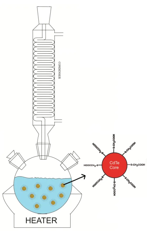
2.1.2 Synthesis of Water Soluble Quantum Dots
For the synthesis of water soluble QDs made of CdTe, we first prepare main precursors including cadmium perchlorate hexahydrate (Cd(ClO4)2.6H2O) for
Cd and aluminum telluride (Al2Te3) for Te. Thioglycolic acid (TGA-
SHCH2COOH) serve as the surfactant and stabilizer, sulfuric acid (H2SO4) as
the reactant to obtain H2Te to transfer Te, sodium hydroxide (NaOH) to regulate
pH, and deionized water as our main solvent. As the main synthesis apparatus, reaction takes place, we need two flasks (1 liter one for the main synthesis and 25 mL one for the H2Te reaction) together with a condenser, a heater, an inert
gas source, and a glass link between flasks, syringe, and septas.
We can divide this synthesis procedure into three main parts. We will introduce them briefly highlighting important points for the synthesis process.
a. Preparation of the main solution
In the beginning, we put 250 mL deionized (DI) water into 1 L flask and then add 4.59 g Cd(ClO4)2.6H2O into water and stir the solution. Observing a
transparent solution indicates the complete dissolution of the Cd-precursor. After this step, we add 1.33 g of TGA with 250 mL of DI water. The ratio of TGA:Cd+2 is extremely important for stability and determines the quality of nanocrystals to affect the reaction between Cd and Te. Later, we inject 0.5 M NaOH solution drop by drop into solution to set the pH of the solution between 11.8 and 12.0 to provide optimum conditions for the synthesis. The prepared solution and reaction set up are illustrated in Figure 2.2.
b. Setting up the mechanism to transfer Te into solution
At this step, we transfer all needed precursors into the main solution. For that, first, we take 0.8 g of Al2Te3 from the glove box into a 25 mL 3-neck glass flask
without allowing for any reaction with oxygen. Later, we set up the mechanism given in Figure 2 to obtain Te gas and provide it as the main precursor for the main reaction of QD growth. After setting up the system, we flow Ar for 1 h to remove all possible oxygen molecules to prevent oxidation of Cd.
After 1 h, we decrease Ar flow and attach rubber tube to the synthesis setup to prevent leakage of dangerous H2Te gas. Subsequently, we take 10-12 mL of 0.5
M H2SO4 into along syringe and inject it into Al2Te3 drop by drop and very
slowly and wait for 30 min till all H2Te’s transferred into the main solution.
The chemical reaction taking place of when we drop sulfuric acid into aluminum telluride is given by in Equations (2.9) and (2.10). For a high-quality reaction, dropping sulfuric acid slowly and waiting for a while after injection until reaction finishes is important.
(2.9) (2.10)
Figure 2.2. Synthesis setup to remove oxygen from the system and injection of sulfiric acid to
obtain and transfer H2Te into the main solution.
c. Heating and observing the change in the reaction mixture
After disconnecting the little flask, we can start heating the mental to provide the necessary energy for the reaction. With boiling at around 100oC, the reaction
starts and CdTe QDs start to grow. We take samples at diferent time intervals and check the emission of the reaction solution to verify that the synthesis process is going fine and QDs grow as expected. The growth reaction is given in Equations (2.11) and (2.12). Here SR represents SHCH2COO- part of TGA. The
growth of green CdTe QDs occurs in about 5 minutes. Therefore, a very fast cooling is needed to obtain green CdTe QDs. For the red CdTe QDs, depending on our desired emission wavelength, we may have to wait 1 or 2 days.
The setup used for colloidally synthesized CdTe QDs with TGA ligands are illustrated in Figure 2.3. These synthesized CdTe QDs involve only one type of core material surrounded with ligands.
(2.11)
Figure 2.3. Synthesis setup where the main reaction takes places and the growth of QDs occurs.
2.1.3 Optical Properties of QDs 2.1.3.1 Absorption
In physics, absorption can be described as a fundamental process by which the energy of a photon is absorbed by a matter. In this case, the energy of electron is increased.
Absorbance (A) shows how well a medium absorbs incident light by using the ratio of intensity of incoming light compared to the light departing from the medium. In Figure 2.4, the decrease in optical intensity through the material is illustrated. Absorption coefficient ( ) is absorbance per unit length. Absorbance is a unitless scale whereas the absorption coefficient has the units of cm-1.
Figure 2.4. Illustration of absorbance measurement in which the number of arrows denotes the
intensity of light.
In general, when showing the absorption properties of a medium, the absorbance spectrum is used as a function of wavelength.
(2.13)
In Equations (2.13) and (2.14), and are the intensities of the incoming
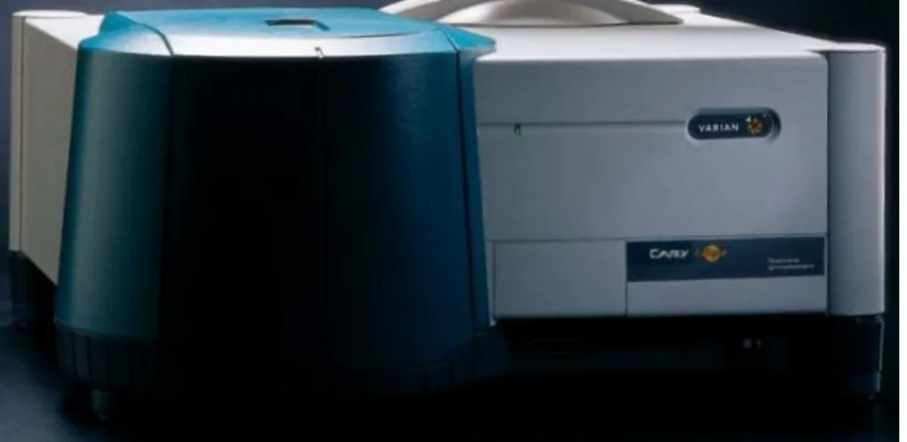
and departing light, T is the transmittance through a medium, %T is the percent transmittance signal and is the length of the path over which absorption takes place. The instrument we used for the absorbance measurement is photographed in Figure 2.5.
Figure 2.5. Varian Cary 5000 UV/vis/NIF spectrophotometer.
Molar extinction coefficient (ε) is also an important metric to quantify the absorption of light per unit concentration per unit length, and can be calculated by using the Beer-Lambert law [26]. According to the Beer-Lambert law, the absorbance is proportional to the multiplication of measurement path length and concentration. The ratio between these gives a molar extinction coefficient at specific wavelength as given in Equations (2.15) and (2.16).
In Equations (2.15) and (2.16), 𝜖 is the molar extinction coefficient at a wavelength of , is the path length over which the absorption takes pace, and C (2.15) (2.16)
is the concentration of the solution. The molar extinction coefficient can be obtained using excitonic peaks based on empirical formulas obtained by prior experiment with proper fitting functions. These derivations are explained in detail in Reference [27, 28].
2.1.3.2 Photoluminescence
Photoluminescence (PL) is the emission of light as a result of optical pumping. We measure the photoluminescence of our samples using a Varian Cary Eclipse Luminescence spectrometer shown in Figure 2.6.
Figure 2.6. Varian Cary Eclipse luminescence spectrophotometer located in UNAM
2.1.3.3 Quantum Yield
By definition, quantum yield ( ) is the ratio of photons absorbed to photons emitted as a result of fluorescence as given in Equation (2.17).
2.1.3.3.1 Measurement of Quantum Yield
To calculate the quantum yield of synthesized quantum dots, we use a reference dye, Rhodamine 6G (Rh 6G), whose quantum yield is a well-known quantity 95% between the wavelengths of 460 and 480 nm.
First, we adjust the absorbance of QDs by changing its concentration to set the crossing of the absorbance curve of Rh 6G with that QDs between 460-480 nm. To minimize self-absorption the intersection point should have absorbance value less than 0.1. At this intersection point, the QDs and reference have the same number of photon’s absorbed for both samples. The intersection of the absorption curves of Rhodamine 6G and green CdTe QDs is presented in Figure 2.7.
Figure 2.7. Absorbance curves of Rh 6G and green CdTe. The crossing point is between 460
and 480 nm where the quantum yield of Rh 6G is 95%. The absorbance is kept below 0.1 to prevent significant self-absorption.
As a second step, we take photoluminescence measurements by exciting our QD sample and the reference dye at the same wavelength of their absorbance crossed. By taking the integral to calculate the area under photoluminescence curve for each of them, we obtain the relative number of emitted photons for both samples. By using the result of integrals and knowing the same absorbance value for both the QDs and dye, we find the ratio between their quantum yields. Since we know the quantum yield of the dye, we can easily calculate the quantum yield of the QD as given in Equation (2.18).
where the QDs and Rh 6G are excited at the wavelength where AbsQD = Absdye .
In Equation (2.18), and are the quantum yields of Rh 6G and the QDs
and similarly, and are the PL of the Rh 6G and the quantum
dots. In Figure 2.8, an example of quantum yield calculation is given.
Figure 2.8. PL of Rh 6G and green CdTe QDs when they are excited while having the same
absorbance value between 460 and 480 nm. The area under the curves shows the total emission (2.18)
2.1.3.4 Time Resolved Flourescence (TRF)
Time-resolved fluorescence spectroscopy is a type of fluorescence spectroscopy used to reveal the emission kinetics of a sample under test. It is a very common technique employed to investigate interactions of organic and inorganic fluorophor molecules and fluorescent materials [29, 30, 31]. In this method, we excite the sample with laser pulses or a pulsed flash light and observe the decay of emission in time by counting photons that hit the detector in time and recording their annual time with respect to the pulse [32]. While taking measurements, because of the bandwidth of the laser pulse we use, we need to deconvolve the measurement results with the response of the source pulse (impulse response function, IRF) to obtain emission kinetics of the sample.
By modeling the decay data with a proper fitting function, we can analyze the experimental results and obtain lifetimes. The fitting is carried out by making use of exponential functions. First, the number of emitted photons is correlated with the number of excited electrons. Second, the number of emitted photons in a time interval is proportional to the change in the number of excited electrons in that time interval. From these two relationships, we arrive at a conclusion that the number of emitted photons in a time interval is proportional to the change in the total number of emitted photons. This relationship is expressed in the Equation (2.19).
where n is the number of excited elements, is the rate constant of emission, and is the arbitrary funciton of time expressing excitation. Assuming excitation occurred at t=0, Equation (2.19) turns into Equation (2.20), which describes this decrease in the number of excited electrons at each point in time.
By solving Equation (20) and taking the integral we obtain Equation (21),
where 𝑛 and 𝑛 describe the number of excited electrons at the beginning and after a time duration, respectively, and ζ is the time constant at which the number of excited electrons drops to 1/e of its maximum.
By using a fixed maximum count, we send an optical excitation pulse and then collect emitted photons as a function of time and repeat these steps until reaching the fixed count. As the set point for the maximum count increases, our results become more reliable because the signal-to-noise ratio is enhanced. In our experiments, we take 𝑛 as the maximum total count, and 𝑛 is the total count after time duration. A TRF decay curve is shown in Figure 2.9.
Figure 2.9. TRF decay curve
However, in our experiments, we do not have only one exponential component (2.20)
(channels) changing the overall rate constant such as nonradiative channels abd energy transfer. Therefore, we make use of a numerical fitting method employing multi-exponentials and then calculate their intensity-averaged or amplitude-weighted lifetime. The model using multiple rates based on the multi-exponential fit is shown in Equations (2.22), (2.23) and (2.24).
To calculate the amplitude-averaged lifetime, we use Equation (2.25).
We carry out our experiments using PicoQuant’s PicoHarp 300. A time correlated single photon counting system (TCSPC) is shown in Figure 2.10. The fitting is carried out by using Fluofit software developed by the PicoQuant.
Figure 2.10. Picoquant Fluotime 200 lifetime spectrometer and Picoharp 300.
(2.22)
(2.23)
(2.24)
Chapter 3
Macrocrystals (MCs)
3.1 Background
A crystal can be defined as a solid in which atoms are placed in a long range order providing an arranged periodic pattern in all three spatial dimensions. The smallest repetitive structure that shows the periodicity and defines crystal structure is called the unit cell. We can classify crystals into groups in terms of different unit cells. There are 7 types of main unit cell shapes and 14 Bravais lattices to support the crystal structure. They are shown in next section of thesis. Another important way of classifying crystals is their physical and chemical properties. They can be divided into four main groups in terms of these features and these make the main features of crystals. The first group is the covalent crystals, which are the ones including only covalent bonds between atoms in their structure. They have in general high melting points. Diamond and zinc sulfide are two common examples of it. The second group is the metal crystals, in which only metal atoms are placed in their lattice structure where electrons are free to move. The third group is the ionic crystals, which have strong ionic
and are very hard materials. The last group is the molecular crystals in which weak bonds such as van der Waals and hydrogen bonds hold crystal together. They consist of molecules. Sugar is a common example of it. There are also crystals, which are more complicated, and include more types of bonds inside and exhibit different properties.
In this thesis, we focus on mainly ionic, molecular, and some common complex crystals. We look for crystals that are water soluble so that they can be ionized in water with ionic or hydrogen bonds. In the later sections of the thesis, the reason of this choice will be explained clearly.
3.1.1 Crystal Planes and Growth Mechanism
According to atom stocking in crystal structures, there are 7 generic unit cell and 14 Bravais lattices showing placement of atoms in these crystal lattices, which are presented in Figure 3.1. Especially, atom bonds and placements in crystal lattice determine the features of the crystal. Miller indices are defined to show the direction from where we look at and planes which are perpendicular to that direction on which atoms are positioned.
Figure 3.1. Crystal tructures and bravais Lattices [33]
3.1.2 Showing directions and planes with Miller Indices
First, we determine three main axis coordinates, which pass over three main edges of the unit cell as a, b, and c. These coordinate systems start from where the edges of the unit cell are intersect at (0,0,0) and continue in positive direction over the edges. The vectors coinciding with these edges on those axes are defined as a1, a2, and a3 unit vectors, each of whose length is set to be 1 on
this coordinate system. Miller directions are defined as a vector using these start point as the origin (0,0,0) and where the vector (or projection of the vector) intercepts the unit cell. We show the coordinates by writing in a bracelet without
planes show the planes of a unit cell. They are determined by the reciprocals of intercept points on the axis and written in parenthesis without any symbol between numbers.
Figure 3.2. Miller directions and planes.
3.2 Crystal Structures of Water Soluble MCs
3.2.1 Properties of Ionic Salt Macrocrystals
Ionic salt crystals occur when positive and negatively charged ions come together in an arranged way. In these structures, the number of total charges is always zero and each ion is surrounded by oppositely charged ions and the whole structure creates a lattice. The simplest example of ionic salt crystals is sodium chloride, which involves Na+ and Cl- ions. The lattice structure of this
Figure 3.3. Crystal lattice of NaCl.
These crystals are water soluble in general since water has polar properties and can pull ions from crystal and let them ionize. Because of having strong electrostatic bonds, these crystals are very hard and strong and disturbing these tight bonds needs a lot of energy. These bonds, surrounded by other ions tightly, cause the crystal to break down suddenly left being cleaved with a sharp edges since they have tight lattices and they provide protection for QDs when incorporated in them.
3.3 Characterization of Crystals
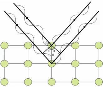
3.3.1 X-Ray Diffraction (XRD) Analysis
X-Ray diffraction method is used to analyze crystal structure of materials by sending X-ray light to sample under test and looking at the diffraction pattern. The wavelength of X-ray light is quite close to the sizes of atom. Therefore, the Bragg reflection occurs when X-ray light hits the atoms. The schematic of atoms placed in a crystal lattice and the Bragg reflection of X-ray light from atoms is presented in Figure 3.4. Reflections coming from those atoms interfere destructively or constructively [34-35].
Figure 3.4. Principle of X-Ray diffraction.
Tpath difference between the X-ray beams is 𝑖𝑛 , where d is the spacing between the atoms in lattice and is the incident angle of the incoming X-ray. So, when this path difference is equal to the wavelength as shown in Figure 13, they have constructive interference. It is also valid when the path difference become integer multiples of wavelength and the mainte general condition for this is given in Equation (3.1).
There are two types of XRD methods depending on the type of crystal: single crystals and powders of polycrystals. In single crystal XRD, we have to use a single crystal and when we send an X-ray light, we see only a few spots on the detector end, which looks like the one where a diffraction grating is placed in front of light. However, in powder XRD measurement, because of having diffractions of many different crystals in different directions and sizes, we end up with rings on the detector and look at just a cross-section of rings. The instrument we used for powder XRD analysis in our measurements is shown in (3.1)
Figure 3.5. Panalytical X’pert Pro Multipurpose X-ray Diffractometer (MPD) located at
UNAM.
Depending on the incident angle of X-ray beam, crystal planes and their lattice distances, we observe peaks where constructive interference occurs. The position of peak gives information about the spacing of atoms and the crystal plane. The area under the peaks gives information about contents of unit cells and phases if it is a mixture. The bandwith and shape of peaks describe the crystallite size and defects. An example of XRD analysis result is shown in Figure 3.6.
3.3.2 Transmission Electron Microscopy (TEM) Analysis
We can think of TEM as a complex version of light microscopy. The main difference between them is to send an electron beam in TEM instead of light beam for high resolution. The working principle is quite similar, like using a series of lenses to magnify the image, and a proper arrangement of lenses to see diffraction patterns and then to transfer the image with magnification; however, these lenses and other parts of devices are complex components to direct electron beam with electromagnetic coils and also need a very powerful vacuum system and a high eV source to accelerate the electron beam.
TEM has different operation modes and features, which enable to make a much detailed analysis such as understanding formations of crystal structures, or to analyze used materials. For example, to look at a sample in diffraction mode helps to see its atoms placement in the lattice. Also, different spectroscopy features help us to understand the material amount at different parts of a sample and focus on the desired parts including a energy dispersive (X-ray) spectroscopy (EDS) and electron energy-loss spectroscopy (EELS). The instrument we have used in our experiments and the main operations of TEM are presented in Figure 3.7.
Figure 3.7. a) FEI Technai G2 F30 TEM located at UNAM and b) the main functions and basic
operating principle of TEM [36].
3.3.3 Scanning Electron Microscope (SEM) Analysis
SEM is an electron microscope like TEM; however, instead of sending an electron beam to an area and detecting the ones passing from it, the electron beam focuses on a spot and then scans the sample by detecting back-scattered electrons. In SEM measurement, surface of the sample has to be electrically conductive, grounded and the material has to be hard and fixed. The measurement gives information about surface topology of the material. The SEM we have used in our measurements is shown in Figure 3.8.
Chapter 4
LED Lighting
4.1 White Light Emitting Diodes (WLEDs)
Within a short period of time, it is expected to see the dominance of solid-state lighting technology thanks to its superior features such as low energy consumption, long lifetime, strong emission and compatibility to current chip technology. WLEDs have already become the main light source of electronics and screen technologies. Some auto manufacturers have started to use WLEDs in headlights of their cars and this is spreading very quickly to other sectors. In this part of the thesis, we will review the basic operating principles of WLEDs and some current LED technologies and will introduce the characterization tools to obtain high quality and efficient illumination with WLED.
4.1.1 How to Generate White Light
Color (Chromaticity)
intrinsic feature of the substance since illuminating light is important for perception. For example, when illuminating a red apple with sunlight, we can see red. However, when we illuminate it with a low pressure sodium lamp, we can see its color changed to yellowish or grayish. We can easily see how important the illumination is for our perception.
Our eyes can sense light between 380 and 700 nm, known as visible spectrum. In this range, we have different sensitivities to light at different wavelengths and can see only the mixture of colors according to our perception. At the same time, our eyes cannot separate at which frequencies the stimulus is, so we can perceive the same color with polychromatic light having different spectrum characteristics. It means that we can apply different light sources whose unique spectral distribution of power (SDP) is suitable obtaining the same color perception.
4.1.2. Different White Light Sources
As a traditional and primitive white light source, the “kerosene lamp”, or “paraffin lamp”, comes to mind, which takes advantages of combustion of oil. It does not have good photometric qualities; however, it is still the main source for many places where electricity is not available. Another traditional source and previously one of the most common one is the incandescent lamp. It is simply the blackbody radiation of tungsten filament heated with electricity. It has the highest color rendering index (CRI) since they can depict the real colors of the illuminated object, but its luminous efficacy is very low because of its low efficacy, it was banned in many European and Latin American countries and soon different restrictions will come into force by many other countries.
Fluorescent lamps make presently the most common class of white light sources thanks to having better luminous efficacy compared to incandescent lamps. However, the quality of light remains poor. At the same time, fluorescent lamps involve mercury, which is harmful for the environment. Solid state lighting offers a big potential in replacing the conventional light sources thanks to its superior features in terms of energy efficiency, color quality, strong emission and easy integration to current semiconductor chip technology.
Spectra of traditional incandescent and fluorescent light sources together with sunlight and phosphor LEDs are presented in Figure 4.1. The differences on their spectra determine the colorimetric properties of these sources and effect the visual perception.
4.1.2 Measurement Methods and Comparisons of Light
SourcesTo evaluate the color quality and photometric efficiency, white light sources should be analyzed in a quantitive manner. For this purpose, The International Commission for Illumination (Commusion Internationale de l’Eclairage, CIE) published a report presenting a standardized method for the definition of color. CIE determined three color matching functions, x, y, and z, which are shown in Figure 4.2.
Figure 4.2. CIE Color matching functions [38].
The method introduced by CIE uses three color matching functions and a chromaticity diagram. The three tristimulus values, X, Y, and Z show the amount of the color stimulus by using these color matching functions and the spectral power distribution of light. X, Y, and Z values are calculated through Equations (4.1), (4.2) and (4.3) [37, 39].
(4.1)
4.1.2.1 Chromaticity Coordinates
Chromaticity diagram uses calculated tristimulus values to define the coordinates via using a mapping method enabling to present the color information in terms of two parameters instead of three by considering their relative ratios among each other. The calculations are shown in Equations (4.4), (4.5) and (4.6) [37,39,40].
According to the calculated (x,y) values, the chromacity diagram, or color coordinates, defined by CIE is shown in Figure 4.3.
(4.3)
(4.4)
(4.5)
Figure 4.3. CIE 1931 (x, y) Color Coordinates [41].
.
Although CIE 1931 is used frequently, this approach lacks the ability to correlate the color differences with a color distance difference. To fix this problem, CIE presented new chromaticity diagrams in 1960 and 1976 as (u, v) and (u’, v’), respectively.The color coordinates of (u’,v’), shown in Figure 4.4, are calculated by using these tristimulus values in different ratios, as given in Equations (4.7), (4.8) and (4.9) [37,39,40].
(4.7)
(4.8)
Figure 4.4. CIE 1976 (u', v') color coordinates [42].
4.1.2.2 Color Rendering Index (CRI)
Color rendering index (CRI) is the widely accepted metric quantifying the color rendering performance of light sources by comparing of the color of an object under a test light source and a reference illuminant. CRI takes a value between 100 and -100 and a higher number indicates a more successful color rendering performance.
To calculate general CRI, 8 general test samples are illuminated under the test and the reference illuminant. The chromaticity differences between the reflections from the samples are used in the calculations.
The first step is to calculate three tristimulus values and find their coordinates in the chromaticity diagram of (u,v) according to 1960 CIE standards.
Subsequently, we convert them into (c, d) coordinates by using Equations (4.10) and (4.11) and will use those parameters in next parts of calculation [39,40].
Here, we use “r” and “t” subscripts to denote these values belong to either the reference or the test, respectively, and “i” subscript to specify which test sample we illuminate [39, 40]. The calculations of , , and are given in
Equations (4.12), (4.13), (4.14), and (4.15). (4.10) (4.11) (4.12) (4.13) (4.14) (4.15) (4.16) (4.17)
After obtaining these values, we can calculate the color shift indicated as using Equation (45) [39, 40].
As a final step, we find the CRI for each sample and take their average using Equations (4.20) and (4.21) [39, 40].
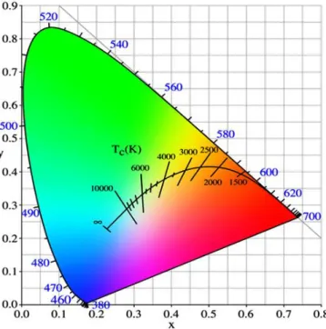
4.1.2.3 Correlated Color Temperature (CCT)
Correlated color temperate is a very commonly used quantity used to compare lighting sources with the light generated by a blackbody radiator. By definition, a blackbody absorbs and does not emit light at -273.15 K, which would then appear black and when heated, it radiates light in accordance with the blackbody radiation law. The blackbody radiation at different temperatures is shown in Figure 4.5 and the radiation spectrum is modeled in Equation (4.22) [39].
(4.18)
(4.19)
(4.20) (4.21)
Figure 4.5. Blackbody radiation spectra [39].
In Equation (4.23), h is the Planck’s constant, k is the Boltzmann’s constant, c is the speed of light, is the wavelength, and T is the absolute temperature in terms of K and the peaks of radiation are determined by Equation (4.24) [39].
According to its temperature, a blackbody radiator, radiates light in different colors (at different wavelengths). When the temperature of the blackbody radiator is increased, the color of the light becomes bluish and seems colder. When it is heated more, the color shifts further to blue. According to the blackbody radiation, the color temperature is defined for the color of light at which temperature the blackbody radiator emits. However, the Planckian locus describing the blackbody radiation makes only a curve on the color gamut. To compare other colors, a correlated color temperature is defined to find the closest point on the Planckian locus corresponding to the most similar light a (4.23)
Figure 4.6. We can see the color dependence on the temperature and it is opposite to the common judgment that higher CCT means colder bluish colors as shown in Figure 4.6 and Figure 4.7.
Figure 14.6. Planckian locus and constant CCT lines ]39].
4.1.2.4 Luminous Efficacy of Optical Radiation (LER)
Light is also an electromagnetic radiation. Therefore; it can be described in terms of consumed and dissipated power with radiometric units. However, we have to consider the sensitivity of human eye since the perception level will change depending on the color content as presented in Figure 4.8. Hence, photometric quantities are introduced by taking this phenomenon into account.
Figure 4.8. CIE 1978 eye sensitivity function [39].
The radiant flux ( 𝑅) defines the total of amount of light radiated by a light
source. To find the luminous flux, we weight the radiant flux with the eye sensitivity function (V and integrate it across the spectrum and the calculation of luminous flux is given in Equation (4.25) [39,40].
Luminous efficacy of optical radiation (LER) is the ratio of the luminous flux to the radiant flux. It is a very important metric since it describes how well the light (4.25)
source produces visible light for a human eye to sense at a given optical power. The calculation of LER is given in Equation (4.26).
4.2. White Light Generation Techniques using LEDs
4.2.1. Principles of LED
Light-emitting diodes make a type of diodes typically in a p-i-n junction architecture that produce light under forward bias conditions as a result of electroluminescence. With carrier injection the minority carrier density is increased in highly doped regions leading to increased recombination of electrons and holes. However, the recombination process is not always necessarily radiative. In some materials, radiative channel is more dominant and these materials are more suitable for producing LEDs. The recombination process under different biases is shown in Figure 4.9.
Figure 4.9. Band diagrams of a) homojunction under no bias b) homojunction under forward
bias, and c) heterojunction with a quantum well under forward bias [39]
To produce an efficient LED at a desired wavelength, we have to take into (4.26)
specific methods such as adding N to create a new energy level and obtain efficient radiative channels. Second, to obtain emission at a desired wavelength we can calculate the photon energy of the targeted emission and match it with the repaired band gap of one of semiconductor materials presented in Figure 4.10. Third, the ability to dope material is quite significant since the carrier density plays an important role. Fourth, with band gap engineering, carriers can be confined in junction region, which increases recombination process in quantum wells. In thesis we used LEDs of indium gallium nitride (InGaN) - gallium(III) nitride (GaN).
Figure 4.10. Energy bandgap diagram and lattice constants of various semiconductors.
4.2.3. Different Approaches for WLEDs
To obtain white light, we need to blend two or more colors. LEDs are quite superior in terms of efficiency, luminous intensity and color quality; however, the emitted light is monochromatic. Hence, to produce white light, as a first approach, we need to use more LED chips or as a second approach, we have to make us of the color conversion technique to obtain other color components.
4.2.3.1 Multi-chip WLEDs
In this approach, we use typically three different LED chips emitting in blue, green and red colors with very narrow bandwidths, so that we can shape the spectrum as we desire. Although WLEDs exhibit good colorimetric and photometric features, and allow for spectral tuning, the cost of production increases tremendously because of the electrical circuitry. Another problem is to obtain the green color since current green LEDs are inefficient.
4.2.3.2 Single-chip WLEDs using Color Conversion Technique
This approach is based on using a single LED chip that emits high-energy photon to optically pump a photoluminescent color-converting material. By employing this approach, by coating a LED chip with color converter materials, we can produce multiple colors and collectively obtain white light emission.
Currently, the most common color-converting materials are phosphors with rare earth elements and QDs since they can be easily integrated to today’s LED fabrication technology and very cost effective. However, for phosphors , most of the source of rare earth elements is under the control of China and sometimes supply chain of those materials becomes a critical problem. Phosphors suffer also the drawbacks of broad emission towards longer wavelengths, leading to limited color quality and tunability. As an alternative material system, QD integrated white LEDs have started to emerge in recent years. They allow for fine-tuning the emission spectra because of their narrow emission bandwidths. Therefore, very high quality white light generation can be realized when QDs are used as color converters. However, to integrate them on a LED chip can become a problem. In this thesis, we will introduce a recently discovered method to integrate QDs embedded in macrocrystals into LEDs, which
Chapter 5
QD Incorporated Macrocrystals
5.1 Principles of QDs embedded in macrocrystals (MCs)
Recently, embedding QDs into MCs has been discovered [8]. Our partner noticed a change when he looked at the forgotten bottle involving a mixture of quantum dots and ionic salts solution. He saw crystal parts at the bottom in different color and they also emitted light under UV light like regular QD. This has led to the idea of incorporating QDs into macrocrystals of ionic salts and showed that QDs are embedded into macrocrystals where they are protected in a poly-crystalline structure and present enhanced optical features including high stability, robustness, and integration capability for LEDs [8].
In this thesis, we have used this method; however, here we have focused on two main points: The first one was to analyze the effect of physical crystal properties depending on the crystal size, material, and structure. Our main purpose was to produce a single crystal in a large size, survey its properties. The second point was to obtain WLEDs using QD embedded MCs as color-converters by coating the directly on LEDs and studying their colorimetric properties. In this chapter, we investigated their physical crystal properties such as size, transparency, and
changes depending on different host materials to improve optical properties and crystal quality for different applications.
5.2 Embedding QDs into Different Host Media
We aimed at understanding the effect of host media and crystal structure. We thought of making big, single crystalline structures instead of poly-crystals of ionic salts to enhance optical properties of QDs.
Existence of common, cheap, easy-to-grow materials for single crystalline structures was another motivation behind this study. We have used Alum (aluminum phosphate), K-Alum (potassium aluminum phosphate), Epsom salt (magnesium Sulfate) and sugar molecules (glucose) for macrocrystal synthesis in the presence of QDs.
In our experiments, we studied controlling and analyzing important parameters including evaporation conditions, concentrations and surface properties of the container while using these highly common and easy-to-grow crystals. We have succeeded at making good macrocrystals of QDs of around a few centimeters in size within a day, although we have noticed some problems.
Epsom crystal is very common material for fast crystal growth. It consists of Mg2+ and SO
42- ions. It grows in shards or spikes. Although it is transparent at
the beginning, it eventually becomes white due to dehydration. In Figure 5.1, we have investigated two different samples of QD-incorporated Epsom crystals to observe the difference as a result of dehydration.
Figure 5.1. Epsom salt crystal samples at the beginning and after dehydration.
Alum crystals are quite common and commercially available material to make single crystals. It involves potassium, aluminum, and sulfate groups inside and its formula is KAl(SO4)2. They are even sold by crystal kits for children to grow
single crystals in a few days. We have made some alum crystals involving QDs for incorporation of QDs finely. However, we have encountered accumulation of QDs in some parts inside the crystals. For a very simple and fast growth, we have used petry dishes because of their hydrophobicity enabling a better crystal quality. We have succeeded to grow 1-2 cm QD-incorporated crystals in a day, which are presented in Figures 5.2, and 5.3.
Figure 5.2. Newly grown samples of Alum crystals, with red CdTe QDs on the left and green

![Figure 3.1. Crystal tructures and bravais Lattices [33]](https://thumb-eu.123doks.com/thumbv2/9libnet/5868172.120798/41.892.278.678.189.706/figure-crystal-tructures-bravais-lattices.webp)
![Figure 3.7. a) FEI Technai G2 F30 TEM located at UNAM and b) the main functions and basic operating principle of TEM [36]](https://thumb-eu.123doks.com/thumbv2/9libnet/5868172.120798/47.892.202.782.193.557/figure-technai-located-unam-functions-basic-operating-principle.webp)
![Figure 4.1. Spectra of different light sources [37].](https://thumb-eu.123doks.com/thumbv2/9libnet/5868172.120798/51.892.196.764.581.1006/figure-spectra-different-light-sources.webp)
![Figure 4.3. CIE 1931 (x, y) Color Coordinates [41].](https://thumb-eu.123doks.com/thumbv2/9libnet/5868172.120798/54.892.332.624.187.513/figure-cie-x-color-coordinates.webp)
![Figure 4.4. CIE 1976 (u', v') color coordinates [42].](https://thumb-eu.123doks.com/thumbv2/9libnet/5868172.120798/55.892.309.646.197.508/figure-cie-color-coordinates.webp)