One and Two Dimensional LiNbO
3
Photonic Crystals
Sevket Simsek
Nanotechnology Research Center (NANOTAM) Bilkent University
06800, Ankara, Turkey [email protected]
Amirullah M.Mamedov, Ekmel Ozbay
Nanotechnology Research Center (NANOTAM)Bilkent University 06800, Ankara, Turkey
[email protected], [email protected]
Abstract—In this report, we present an investigation of the optical properties and band structure calculations for the photonic crystal structures (PCs) based on one-dimensional (1D) and two-dimensional (2D) ferroelectric LiNbO3 crystal. Here we
use 1D and 2D periodic crystal structure of dielectric rods and layers in air background. We have theoretically calculated photonic band structure and optical properties of 1D and 2D LiNbO3 PCs. Beside, we have calculated affect PBG properties of
different parameters such as filling fraction and the shape. In order to get photonic gap map, we have calculated the gaps as a function of radius of the rods. We have also investigated the nature of guided modes in line defect waveguide. In our simulation, we employed the finite-difference time domain (FDTD) technique which implies the solution of Maxwell equations with centered finite-difference expressions for the space and time derivatives.
Keywords—LiNbO3, photonic band structure, transmission
I. INTRODUCTION
Photonic crystals (PCs) are now well acknowledged for their capability to control and manipulate the propagation of electromagnetic waves in confined space [1]. The work of Yablonovitch [2] and John [3] on such structures, often called photonic crystals, displays a range of frequency where propagation is completely forbidden. This is called the photonic band gap (PBG) and is analogous to the electronic band gap that is found in semiconductors. These dielectric materials, with complete band gaps, appear to be promising candidates for next generation optoelectronic devices and a new class of waveguiding [4-6]. Beside, Transmission spectrum of PC waveguide filter is sensitive to refractive index and structural changes induced due to the applied electric field. These kind of tunable optical filters are highly desired for integrated optical communication and light manipulation.
LiNbO3 (LN) is a ferroelectric material. It is highly
piezoelectric and it has interesting properties for the implementation of active PCs. LN has the advantage of a wide electro-optic coefficient [7] and low loss optical propagation. Beside this, LN is also a material extensively used in optoelectronics and surface acoustic wave devices [8]. Due to its high electro-optical, acoustooptical and nonlinear coefficients, LN represents indeed an excellent candidate for the realization of dynamic PhC structures [9].
In this paper, we study a one dimensional (1D) and two-dimensional (2D) photonic crystal square lattice of the LN compound.
II. SIMULATION
A. Finite Difference Time Domain (FDTD)Method
FDTD algorithm is one of the most appropriate calculation tools [12]. For solving Maxwell's equations depending on the time, FDTD algorithm divides the space and time in a regular grid. Perfect matched layers (PMLs) can be used in the determination of the boundary conditions [13]. In general, the thickness of PML layer in overall simulation area is equal to a lattice constant. FDTD solves electric and magnetic fields by rating depending on space and time and deploys that rating in different spatial regions by sliding each field component half of a pixel. This procedure is known as Yee grid discretization. Fields in these grids can be classified as TM and TE polarization.
III. RESULTS A. Photonic Crystals of 1D Layered LiNbO3
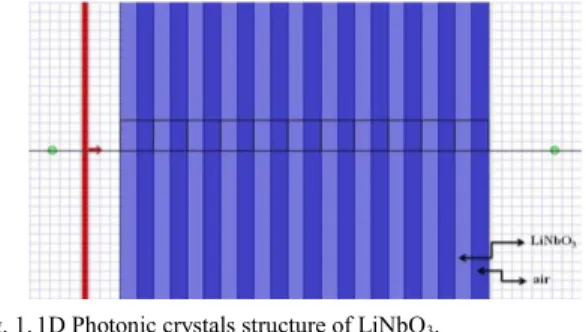
The systematic of a typical 1D PC is shown Fig. 1. 1D photonic crystals are characterized by the refractive index contrast and filling fraction. The refractive index contrast is the ratio of the higher refractive index to the lower refractive index in the multiplexer system. The filling fraction f is the ratio between the thickness of the lower refractive index layer(air) and the period of the PC, i.e., f=d1/(d1+d2). The
calculated band structure and transmission properties of 1D LN/air PCs using the OptiFDTD package [14] is given in Fig. 2 and 3.
Fig. 1. 1D Photonic crystals structure of LiNbO3.
The dielectric constant of LN is taken as ε=5. Results are presented in terms of frequencies ωa/2πc=a/λ, where a is the lattice constant a=1μm, c the speed of light in a vacuum and λ
49
the vacuum wavelength. The thickness of the considered
layers of air and LN ( , )
4 4 air LN air LN d d n n O O are 0.5μm and
0.5 μm. The filling fraction is set to 0.5. The shaded areas illustrate the PBGs.
We can see from Fig. 2 that there are five PBGs situated in the visible, UV, near-infrared regions. The first TM band gaps appeared to be between the first and second bands in the frequency ranges of (0.241–0.367) ωa/2πc, the second band gaps (0.559–0.692) ωa/2πc, the third band gaps (0.921–0.950) ωa/2πc, fourth band gaps (1.180–1.281) ωa/2πc and fifth band gaps (1.472–1.621) ωa/2πc. Their respective widths are 41.4%, 22.8%, 3.76%, 8.20% and 9.57%, respectively.
Fig. 2. TM band sturucture of 1D LiNbO3.
In this frequency intervals no allowed mode and the electromagnetic propagation is not possible within this gap. This means that the photon emitted from the source does not propagate but is strongly localized around the rod including the source, when the photon frequency is within the photonic band gap. This result shows well that if the spectral maximum frequency of the luminescence lies around the centre of a photonic band gap, the luminescence could be suppressed.
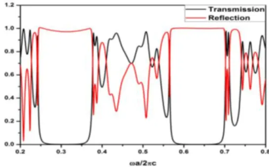
Beside this, one another calculation is realized to detect the frequency of transmission of light across the photonic crystal for the same structure (Fig. 3).
Fig. 3. Transmission and reflection spectrum for 1D LiNbO3 PC.
This transmission characteristic is observed by obtaining transmission spectrum of light in significant number of 1D layers with respect to frequency. The transmission in the structure vanishes between (0.241-0.367) ωa/2πc and (0.559-0.692) ωa/2πc frequency ranges. It means, this frequency range take part in photonic band gap and electromagnetic
waves in this frequency range cannot radiate in this structure. The calculated spectrum shows complete suppression of transmission in the region precisely coincident with the gap in the band structure, clearly demonstrating the effect of photonic bands on the luminescent properties of LN.
In Fig. 4, It is clear that the size of the gap increases with filling factor for the first band gap. The largest gap size is about 50% when filling factor is as high as 0.7, but it decrease when filling factor continues to increase. On the other hand, the second gap size begins to decrease, and the second band closes when filling foctor is 0.7.
Fig. 4. Filling factor for 1D lattice of LiNbO3 B. 2D Square Lattice of LiNbO3 Rods
All calculations in 2D LN were performed using the MIT Photonic Bands (MPB) and Electromagnetic Equation Propagation (MEEP) Package based on finite diffrenece time-domain (FDTD) simulations of arbitrary electromagnetic structure, which can be used to calculate band diagrams and eigenfields for the crystals [10,15,16]. The calculated TM photonic band structure structure, transmission spectrum, photonic band map, group velocity and equi-frequency contours are given in Fig. 5, Fig. 6, Fig .7, Fig. 8 and Fig. 9 , respectively.
Fig. 5. The TM band structure for a square array of dielectric columns for LiNbO3.
In Fig. 5, we present the photonic band structure for the case of H polarization for a square array of dielectric columns of LN when εLN =5, εair =1, and f=0.2826. The solid lines
represent wave vector from Γ to X to measure the corresponding frequencies of the propagating photon. We can see two photonic band gaps in Fig.9. The first TM band gaps appeared to be between the first and second bands in the frequency ranges of (0.353–0.402) ωa/2πc for LN. The second band gap take places in the frequency ranges of (0.619–0.651) ωa/2πc. For the TM modes, this photonic
crystal has a complete photonic band gap (PBG) in the infred region, with a 13.1% and 5.06% gap-midgap ratios. In this frequency intervals no allowed mode and the electromagnetic propagation is not possible within this gaps. This means that the photon emitted from the source does not propagate but is strongly localized around the rod including the source, when the photon frequency is within the photonic band gap.
Beside this, one another calculation is realized to detect the frequency of transmission and reflection of light across the photonic crystal for the same structure (Fig. 6). This transmission characteristic is observed by obtaining transmission spectrum of light in significant number of 2D rods with respect to frequency. The transmission in the structure vanishes between (0.287-0.400) ωa/2πc frequency range. It means, this frequency range take part in photonic band gap and electromagnetic waves in this frequency range cannot radiate in this structure.
Fig. 6. Transmission spectrumu of LiNbO3 rods in square lattice.
The photonic band gap map of LN for the TM polarization presented in Fig. 7 it shows that the spectral width varies with the (r/a) ratio (dielectric rod diameter divided by lattice constant). The existence of a gap, however, depends strongly on r/a ratio which clearly shows that only above a critical value of circular rod size, (r/a ≥ 0.15 for LN) TM photonic gap can be obtained. According to the findings in Fig. 7 is that most suitable (r/a) ratio value is 0.25a for LN. Changes in rod diameter and lattice constant can serve to fabricate different useful optical devices. The gap map could be useful in the design of LN rod photonic crystal light emitting devices.
Fig. 7. Photonic band map of LiNbO3 rods in square lattice.
Fig. 8 shows group velocity distribution of LN. However, group velocity decreases dramatically as the mode approaches from the center of the Brillouin zone (Г) to the (X) boundary which indicates a slow wave behavior. It is worth noting that group velocity is zero between (X) and (M) boundaries. The
region between these two boundaries falls in the region of PBGs.
Fig. 8. Group velocity of LiNbO3 rods in square lattice.
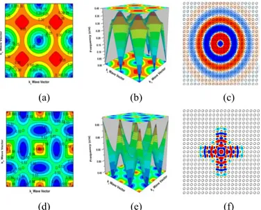
Fig. 9 shows the calculated equi-frequency contours for TM1 and TM2 bands. Equi-frequency or isofrequency contour is helpful in analyzing behaviors of photonic crystals, which is the intersection of a constant frequency ω-plane to a dispersion surface [17]. It quantifies all allowed wavevectors in the photonic crystals and their corresponding frequencies.
Just like band-structure, iso-frequency contour can also be used to describe the dispersion of waves propagating in periodic structures. In momentum k space, iso-frequency contour or iso-energy contour consists of all the terminals of wavevectors corresponding to same frequency or same energy. Almost all the properties of waves propagating in the periodic structure can be deduced from the iso-frequency contours. For instance, the negative refraction and selfcollimation of light are all directly linked with the iso-frequency or energy contour in photonic crystals. Therefore, the determination of iso-frequency contour is crucial to understand properties of photonic crystals[18].
(a) (b) (c)
(d) (e) (f)
Fig. 9. Contour structure of LiNbO3 rods in square lattice. Contour structure for TM1 band in 2D (a) and 3D (b), contour structure for TM2 band in 2D (d) and 3D (e).
A perfect circular equi-frequency contour means that light can travel isotropically. A square-like equi-frequency contour can be used to harvest its collimation property
collimation), and a star-like contour may be used in designing high-dispersive elements (superprism) that can support many channels in optical communications. In such as a square-like contour or a star-like equi-frequency contour situations, the photonic crystals shows strong an-isotropic property [19]. The calculated equi-frequency contours for TM1 and TM2 bands are given in Fig. 9(a) and Fig. 9(d), respectively. Light travel isotropically since equi-frequency contour has a circular form as seen in Fig. 9(a). However, we can see in Fig. 9(d) that equi-frequency contour has a square-like contour. It means that light can travel without scattering. As seen in figure 9(c), When we place the point source with normalized frequency ω=0.15 (2πc/a) at the centre of the structure to excite the mode, the light propagate isotropically as if it propagates in a homogeneous material. On the other hand, When we also place the point source with normalized frequency ω = 0.59 (2πc/a) at the centre of the structure to excite the mode, we see that the light is confined mainly along the x and y directions, as given in figure 9(f). One can deduced from fig. 9(c) and fig. 9(f) that a selfcollimation phenomenon is observed. These results show obviously that above our FDTD simulations are correct.
C. Line Defect Structure of 2D LiNbO3 Photonic Crystal
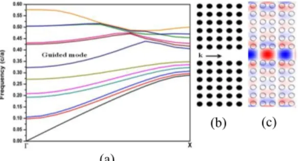
Using lineer defects, light can be guided from one location to another [1]. The basic idea is to create a linear waveguide by removing a linear sequence of unit cells from perfect photonic crystal, as seen in Fig. 10 (b). The dispesion diagram of TM polarized photonic crystal waveguide is given in Fig. 10 (a). Because of line defect, we can see a discrete guided band within the TM band gap as seen in Fig. 10 (a). The mode expressed by this band is evanescent within the crystal and is localized within the defect. Thus, light can be guided along the defect as shown in Fig .10 (c). The gap is centered at frequency of 0.398 ωa/2πc.
Fig. 10. Line defect TM band structure of LiNbO3 rods in square lattice (a), Line defect photonic crystal structure of LiNbO3 rods in square lattice (b), Electromagnetic wave propagation in line defect structure of LiNbO3 rods in square lattice (c).
IV. CONCLUSION
In conclusion, the photonic band structures and transmission properties of the 1D and 2D lattice of the LN PCs consisting of dielectric rods and layers immersed in air were studied. The calculated results show that a large PBG can be produced in square lattice by using 1D layers and 2D cylindrical rods. We have outlined basic properties of band gap guiding PCs and have discussed according to LN lattice.
These simulated results should be useful in the design of 1D and 2D LN based PCs when a large PBG is desired. Furthermore, LN has high bandgaps and thus are highly transparent in the visible range, which is very important for any application in this spectral region. Due to the photonic band gap effect, the luminescence of 1D and 2D LN can be suppressed or enhanced. The controllable luminescence of LN rods can be useful in the implementation of efficient LN rod light emitting devices.
REFERENCES
[1] J. D. Joannopulous , R. D. Meade, J. N. Winn, Photonic Crystals: Molding the Flow of Light, 2nd ed., Princeton University Press. 1995. [2] E. Yablonovitch, “Inhibited spontaneous emission in solid-state physics
and electronics” Phys. Rev. Lett., vol. 58, pp. 2059-2062, 1987. [3] S. John, “Strong localization of photons in certain disordered dielectric
superlattices” Phys. Rev. Lett., vol. 58, pp. 2486-2489, 1987.
[4] K. Sakoda, Optical properties of Photonic Crystals, 2nd edn. Springer 2001.
[5] S. Fan, J. N. Winn, A. Devenyi, J. C. Chen, R. D. Meade, J. D. Joannopoulos, “Guided and defect modes in periodic dielectric waveguides ”J. Opt. Soc. Am. B.,vol. 12, pp. 1267-1272, 1995.
[6] S. Li and Y. Y. Lu, "Efficient Method for Computing Leaky Modes in Two-Dimensional Photonic Crystal Waveguides," J. Lightwave Technol. Vol. 28, pp. 978-983, 2010.
[7] M. Roussey, M.-P. Bernal, N. Courjal, D. Van Labeke, F. I. Baida, and R. Salut, “Electro-optic effect exaltation on lithium niobate photonic crystals due to slow photons” Appl. Phys. Lett. Vol. 89 (24), pp. 241110-241113, 2006.
[8] N. Courjal, S. Benchabane, J. Dahdah, G. Ulliac, Y. Gruson, and V. Laude, “Acousto-optically tunable lithium niobate photonic crystal”, Appl. Phys. Lett. Vol. 96(13), pp. 131103-131106, 2010.
[9] N. Courjal, M. P. Bernal, G. Ulliac, J. Dahdah, S. Benchabane, J-M. Merolla,“LiNbO3 acousto-optical and electro-optical micromodulators”, Journal of the European Optical Society vol. 4, pp. 09018- 09026, 2009. [10] M. Roussey, M-P. Bernal, N. Courjal, and F. I. Baida, “Experimental
and theoretical characterization of a lithium niobate photonic crystal”, Applied Physics Letters, vol. 87, pp. 241101-241103, 2005.
[11] M. Plihal and A. A. Maradudin, “Photonic band structure of two-dimensional systems: The triangular lattice”Phys. Rev. B vol. 44, pp. 8565-8571, 1991.
[12] Taflove A. and Hagness S. C. 2000 Computational Electrodynamics: The Finite-Difference Time-Domain Method 2nd edn (Boston, MA: Artech House Publishers).
[13] Jean-Pierre Berenger, “A Perfectly matched layer for the absorption of electromagnetic waves”J. Comput. Phys. Vol. 114 ,pp. 185–200, 1994. [14] OptiFDTD 10, http://www.optiwave.com/
[15] S. G. Johnson, J. D. Joannopoulos, The MIT Photonic-Bands Package (http://ab-initio.mitedu/mpb/).
[16] A. F. Oskooi, D. Roundyb, M. Ibanescua, P. Bermelc, J. D. Joannopoulosa, S. G. Johnson, “MEEP: A flexible free-software package for electromagnetic simulations by the FDTD method”, Computer Physics Communications, vol. 181, pp. 687-702 ,2010. [17] Dennis W. Prather et al, Photonic crystals: theory, applications, and
fabrication, Wiley, 2009.
[18] Lei Shi, Haiwei Yin, Xialong Zhu, Xiaohan Liu, Jian Zi, “Direct observation of iso-frequency contour of surface modes in defective photonic crystals in real space”, Applied Physics Letters, vol. 97, pp. 251111-251114, 2010.
[19] Guilin Sun and Andrew G. Kirk,"Analyses of negative refraction in the partial bandgap of photonic crystals," Opt. Express, vol. 16, pp. 4330-4336, 2008.
(b) (a)
(c)