Guiding, bending, and splitting of electromagnetic waves in highly confined
photonic crystal waveguides
Mehmet Bayindir*and E. Ozbay
Department of Physics, Bilkent University, Bilkent, 06533 Ankara, Turkey B. Temelkuran
Department of Materials Science and Engineering & Research Laboratory of Electronics, Massachusetts Institute of Technology, Cambridge, Massachusetts 02139
M. M. Sigalas
Communications and Optics Lab, Agilent Labs, Agilent Technologies, 3500 Deer Creek Road, MS26M9C, Palo Alto, California 94304 C. M. Soukoulis, R. Biswas, and K. M. Ho
Ames Laboratory and Microelectronics Research Center, Iowa State University, Ames, Iowa 50011 共Received 18 October 2000; published 7 February 2001兲
We have experimentally demonstrated the guiding, bending, and splitting of electromagnetic共EM兲 waves in highly confined waveguides built around three-dimensional layer-by-layer photonic crystals by removing a single rod. Full transmission of the EM waves was observed for straight and bended waveguides. We also investigated the power splitter structures in which the input EM power could be efficiently divided into the output waveguide ports. The experimental results, dispersion relation and photon lifetime, were analyzed with a theory based on the tight-binding photon picture. Our results provide an important tool for designing photonic crystal based optoelectronic components.
DOI: 10.1103/PhysRevB.63.081107 PACS number共s兲: 42.70.Qs, 42.60.Da, 42.82.Et, 71.15.Ap
Photonic crystals, in which the propagation of electro-magnetic waves is forbidden for a certain frequency range,1–3provide a promising tool to control the flow of light in integrated optical devices.4,5 Therefore, there is a great deal of interest in developing photonic crystal-based waveguides where one can confine and efficiently guide the light around sharp corners.6–17 Guiding the light without losses, and even through sharp corners using two-dimensional 共2D兲 photonic crystals was proposed theoreti-cally by Mekis et al.6 Later, researchers have reported ex-perimental observation of waveguiding in 2D photonic crystals first at microwave,7 and then at optical frequencies.12–15However, to avoid the leakage problem in 2D structures, either one has to extend the size of the photo-nic crystal in the vertical direction, or use a strong index-guiding mechanism in the vertical direction.15,17
A way to eliminate the leakage is to use a three-dimensional 共3D兲 photonic crystal. Recently, full confine-ment of the EM waves utilizing a 3D layer-by-layer photonic crystal structure has been theoretically studied.10,11Although Noda et al. reported the fabrication of a 3D sharp bend waveguide at optical wavelengths, they have not reported any optical measurements on this sharp-bend structure.16
In this paper, we demonstrated that the guiding, bending, and splitting of EM waves could be achieved in highly con-fined waveguides which were constructed by removing a single rod from a perfect 3D layer-by-layer photonic crystal. The experimental results were in good agreement with a theory based on tight-binding 共TB兲 approximation,9,18,19and the simulation results of Chutinan and Noda.11
In our experiments, we used a layer-by-layer dielectric photonic crystal20 based on square-shaped alumina rods
共0.32 cm ⫻ 0.32 cm ⫻ 15.25 cm兲, with center-to-center
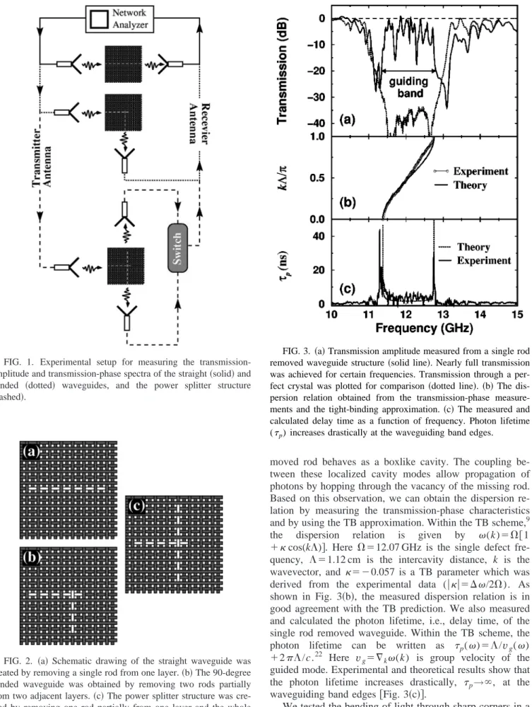
separation of 1.12 cm. The crystal exhibits a three-dimensional photonic band gap with a mid-gap frequency around 12 GHz.21Figure 1 shows the schematics of the mea-surement setup that was used in our experiments. We used an HP 8510C network analyzer and microwave horn antennas to measure the amplitude and the transmission-phase properties of a straight waveguide 关Fig. 2共a兲兴, a 90-degree bended waveguide 关Fig. 2共b兲兴, and a power splitter structure 关Fig. 2共c兲兴. We constructed the straight waveguide by removing a single rod from a single layer of a 6 unit cell
共24 layer兲 photonic crystal, so that we had 12 layers at the
top and 11 layers at the bottom of the removed rod. The polarization vector e of the incident EM wave was kept par-allel to the stacking direction of the layers. We did not ob-serve any guided modes for the other polarization in any of our experiments.
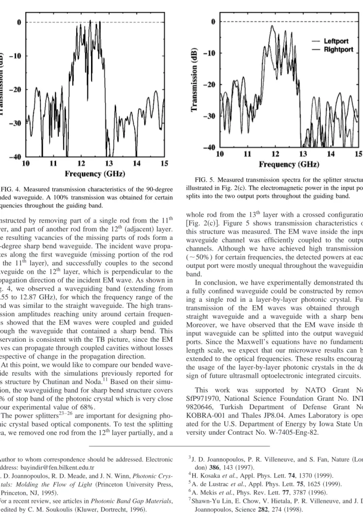
First, we tested the guiding of EM waves by measuring the transmission through a single missing rod. We observed full transmission of the EM waves for certain frequencies within the photonic stop band关Fig. 3共a兲兴. The full transmis-sion within the waveguiding band was a proof of how well the wave was confined and guided without losses. The guid-ing band started from 11.37 GHz and ended at 12.75 GHz. In Fig. 3共a兲, we also plotted the transmission spectra 共dotted line兲 of the perfect crystal for comparison. The guiding was limited with the photonic band gap of the crystal, for which the crystal had the property of reflecting the EM waves in all directions.
In order to understand the underlying physics behind this single rod removed waveguide, we need to closely look at structure of the waveguide. Each vacancy just below the
re-RAPID COMMUNICATIONS
PHYSICAL REVIEW B, VOLUME 63, 081107共R兲
moved rod behaves as a boxlike cavity. The coupling be-tween these localized cavity modes allow propagation of photons by hopping through the vacancy of the missing rod. Based on this observation, we can obtain the dispersion re-lation by measuring the transmission-phase characteristics and by using the TB approximation. Within the TB scheme,9 the dispersion relation is given by (k)⫽⍀关1
⫹cos(k⌳)兴. Here ⍀⫽12.07 GHz is the single defect fre-quency, ⌳⫽1.12 cm is the intercavity distance, k is the wavevector, and ⫽⫺0.057 is a TB parameter which was derived from the experimental data (兩兩⫽⌬/2⍀). As shown in Fig. 3共b兲, the measured dispersion relation is in good agreement with the TB prediction. We also measured and calculated the photon lifetime, i.e., delay time, of the single rod removed waveguide. Within the TB scheme, the photon lifetime can be written as p()⫽⌳/vg()
⫹2⌳/c.22 Here
vg⫽ⵜk(k) is group velocity of the guided mode. Experimental and theoretical results show that the photon lifetime increases drastically, p→⬁, at the waveguiding band edges 关Fig. 3共c兲兴.
We tested the bending of light through sharp corners in a waveguide structure shown in Fig. 2共b兲. This structure was FIG. 1. Experimental setup for measuring the
transmission-amplitude and transmission-phase spectra of the straight共solid兲 and bended 共dotted兲 waveguides, and the power splitter structure 共dashed兲.
FIG. 2. 共a兲 Schematic drawing of the straight waveguide was created by removing a single rod from one layer.共b兲 The 90-degree bended waveguide was obtained by removing two rods partially from two adjacent layers.共c兲 The power splitter structure was cre-ated by removing one rod partially from one layer and the whole rod from the adjacent upper layer.
FIG. 3. 共a兲 Transmission amplitude measured from a single rod removed waveguide structure共solid line兲. Nearly full transmission was achieved for certain frequencies. Transmission through a per-fect crystal was plotted for comparison 共dotted line兲. 共b兲 The dis-persion relation obtained from the transmission-phase measure-ments and the tight-binding approximation.共c兲 The measured and calculated delay time as a function of frequency. Photon lifetime (p) increases drastically at the waveguiding band edges.
RAPID COMMUNICATIONS
MEHMET BAYINDIR et al. PHYSICAL REVIEW B 63 081107共R兲
constructed by removing part of a single rod from the 11th layer, and part of another rod from the 12th共adjacent兲 layer. The resulting vacancies of the missing parts of rods form a 90-degree sharp bend waveguide. The incident wave propa-gates along the first waveguide 共missing portion of the rod on the 11th layer兲, and successfully couples to the second waveguide on the 12th layer, which is perpendicular to the propagation direction of the incident EM wave. As shown in Fig. 4, we observed a waveguiding band 共extending from 11.55 to 12.87 GHz兲, for which the frequency range of the band was similar to the straight waveguide. The high trans-mission amplitudes reaching unity around certain frequen-cies showed that the EM waves were coupled and guided through the waveguide that contained a sharp bend. This observation is consistent with the TB picture, since the EM waves can propagate through coupled cavities without losses irrespective of change in the propagation direction.
At this point, we would like to compare our bended wave-guide results with the simulations previously reported for this structure by Chutinan and Noda.11Based on their simu-lation, the waveguiding band for sharp bend structure covers 67% of stop band of the photonic crystal which is very close to our experimental value of 68%.
The power splitters23–26are important for designing pho-tonic crystal based optical components. To test the splitting idea, we removed one rod from the 12thlayer partially, and a
whole rod from the 13th layer with a crossed configuration
关Fig. 2共c兲兴. Figure 5 shows transmission characteristics of
this structure was measured. The EM wave inside the input waveguide channel was efficiently coupled to the output channels. Although we have achieved high transmission (⬃50%) for certain frequencies, the detected powers at each output port were mostly unequal throughout the waveguiding band.
In conclusion, we have experimentally demonstrated that a fully confined waveguide could be constructed by remov-ing a sremov-ingle rod in a layer-by-layer photonic crystal. Full transmission of the EM waves was obtained through a straight waveguide and a waveguide with a sharp bend. Moreover, we have observed that the EM wave inside the input waveguide can be splitted into the output waveguide ports. Since the Maxwell’s equations have no fundamental length scale, we expect that our microwave results can be extended to the optical frequencies. These results encourage the usage of the layer-by-layer photonic crystals in the de-sign of future ultrasmall optoelectronic integrated circuits.
This work was supported by NATO Grant No. SfP971970, National Science Foundation Grant No. INT-9820646, Turkish Department of Defense Grant No. KOBRA-001 and Thales JP8.04. Ames Laboratory is oper-ated for the U.S. Department of Energy by Iowa State Uni-versity under Contract No. W-7405-Eng-82.
*Author to whom correspondence should be addressed. Electronic address: [email protected]
1J. D. Joannopoulos, R. D. Meade, and J. N. Winn, Photonic Crys-tals: Molding the Flow of Light 共Princeton University Press, Princeton, NJ, 1995兲.
2For a recent review, see articles in Photonic Band Gap Materials, edited by C. M. Soukoulis共Kluwer, Dortrecht, 1996兲.
3J. D. Joannopoulos, P. R. Villeneuve, and S. Fan, Nature 共Lon-don兲 386, 143 共1997兲.
4H. Kosaka et al., Appl. Phys. Lett. 74, 1370共1999兲. 5A. de Lustrac et al., Appl. Phys. Lett. 75, 1625共1999兲. 6A. Mekis et al., Phys. Rev. Lett. 77, 3787共1996兲.
7Shawn-Yu Lin, E. Chow, V. Hietala, P. R. Villeneuve, and J. D. Joannopoulos, Science 282, 274共1998兲.
FIG. 4. Measured transmission characteristics of the 90-degree bended waveguide. A 100% transmission was obtained for certain frequencies throughout the guiding band.
FIG. 5. Measured transmission spectra for the splitter structure illustrated in Fig. 2共c兲. The electromagnetic power in the input port splits into the two output ports throughout the guiding band.
RAPID COMMUNICATIONS
GUIDING, BENDING, AND SPLITTING OF . . . PHYSICAL REVIEW B 63 081107共R兲
8B. Temelkuran and E. Ozbay, Appl. Phys. Lett. 74, 486 共1999兲.
9Mehmet Bayindir, B. Temelkuran, and E. Ozbay, Phys. Rev. Lett. 84, 2140共2000兲; Phys. Rev. B 61, R11 855 共2000兲.
10M. M. Sigalas et al., Microwave Opt. Technol. Lett. 23, 56 共1999兲.
11A. Chutinan and S. Noda, Appl. Phys. Lett. 75, 3739共1999兲. 12T. Baba, N. Fukaya, and J. Yonekura, Electron. Lett. 35, 654
共1999兲.
13M. Tokushima, H. Kosaka, A. Tomita, and H. Yamada, Appl. Phys. Lett. 76, 952共2000兲.
14M. Loncar et al., Appl. Phys. Lett. 77, 1937共2000兲.
15S. Y. Lin, E. Chow, S. G. Johnson, and J. D. Joannopoulos, Opt. Lett. 25, 1297共2000兲.
16S. Noda, K. Tomoda, N. Yamamoto, and A. Chutinan, Science 289, 604共2000兲.
17S. G. Johnson, P. R. Villeneuve, S. Fan, and J. D. Joannopoulos, Phys. Rev. B 62, 8212共2000兲.
18N. W. Ashcroft and N. D. Mermin, Solid State Physics共Sounders, Philadelphia, 1976兲 p. 175.
19N. Stefanou and A. Modinos, Phys. Rev. B 57, 12 127共1998兲; C. Martijn de Sterke, Phys. Rev. E 57, 3502共1998兲; E. Lidorikis, M. M. Sigalas, E. N. Economou, and C. M. Soukoulis, Phys. Rev. Lett. 81, 1405共1998兲; A. Yariv, Y. Xu, R. K. Lee, and A. Scherer, Opt. Lett. 24, 711共1999兲.
20K. M. Ho, C. T. Chan, C. M. Soukoulis, R. Biswas, and M. M. Sigalas, Solid State Commun. 89, 413共1994兲.
21E. Ozbay, J. Opt. Soc. Am. B 13, 1945共1996兲.
22Mehmet Bayindir and E. Ozbay, Phys. Rev. B 62, R2247共2000兲. 23Mehmet Bayindir, B. Temelkuran, and E. Ozbay, Appl. Phys.
Lett. 77, 3902共2000兲.
24J. Yonekura, M. Ikeda, and T. Baba, J. Lightwave Technol. 17, 1500共1999兲.
25R. W. Ziolkowski and M. Tanaka, Opt. Quantum Electron. 31, 843共1999兲.
26
T. Sondergaard and K. H. Dridi, Phys. Rev. B 61, 15 688共2000兲.
RAPID COMMUNICATIONS
MEHMET BAYINDIR et al. PHYSICAL REVIEW B 63 081107共R兲