PROCEEDINGS OF SPIE
SPIEDigitalLibrary.org/conference-proceedings-of-spie
Photonic metamaterial absorber
designs for infrared solar cell
applications
Kamil Boratay Alici
Ekmel Ozbay
Photonic metamaterial absorber designs for infrared solar-cell
applications
Kamil Boratay Alici* and Ekmel Ozbay
Nanotechnology Research Center, Department of Physics, Department of Electrical and Electronics Engineering, Bilkent University, Bilkent, 06800, Ankara, Turkey
Abstract
We propose a metamaterial based absorber design that operates at the infrared regime. The absorption peak was 83.6%. We can incorporate solar-cell layers inside the metamaterial absorber in order to significantly increase solar-cell efficiency.
Key Words: Metamaterials; Solar energy; Resonant Absorption
1. Introduction
Artificial periodic structures composed of subwavelength unit cells exhibit unusual electromagnetic phenomena such as negative refraction and reversed Cherenkov radiation. These metamaterials can provide a magnetic response at nearly any frequency band of the electromagnetic spectrum, which was determined by the unit cell properties [1-4]. The most common unit cell element is a split ring resonator (SRR). At around the magnetic resonance of an SRR medium, effective permeability (µeff) is negative [5-10]. One of the exciting applications of
metamaterials is ultra-thin absorbers. The possible designs and implementations of metamaterial based absorbers have been studied in the literature [11, 12]. In this presentation, we demonstrate a metal backed photonic SRR based metamaterial absorber operating at infrared (IR) frequencies, which can be used to cover solar cells.
Fig. 1. Geometry of the design. Fig. 2. Simulation results
Next Generation (Nano) Photonic and Cell Technologies for Solar Energy Conversion, edited by Loucas Tsakalakos, Proc. of SPIE Vol. 7772, 77721B · © 2010 SPIE · CCC code: 0277-786X/10/$18 · doi: 10.1117/12.860223
Proc. of SPIE Vol. 7772 77721B-1
2. Geometry and spectral response
The geometry of the design is shown in Fig. 1. The E-field of the linearly polarized light is shown with a red arrow. The SRR array that was used in this simulation was fabricated via e-beam lithography and tested experimentally by using a homemade optical transmission setup. The parameters of the SRR array were verified by comparing the simulation and experimental data. We used Palik’s book [13] for the silver (Ag) parameters in our simulations. The response of the medium was simulated by using a commercial full-wave solver. All the details of the SRRs operating at the optical regime including fabrication, measurement and characterization methods are given in our recent study on the basics of photonic magnetic metamaterials [14]. We calculated the complex scattering parameters and plotted the magnitude of transmission (|S21|), reflection (|S11|), and the
extracted absorbance (A) data, as shown in Fig. 2. We obtained an 83.6% absorbance peak at 184.2 THz (1628nm). In Fig. 2, we show a reflection dip at around 185 THz with a 45.7 THz full width at half maximum (FWHM) bandwidth.
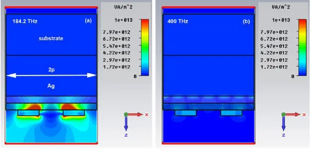
Fig. 3. Power distribution in the vicinity of split ring resonators (a) at 184.2 THz peak absorbance frequency (b) at 400 THz an arbitrary frequency. Two unit cells were shown in each part. The scale of the parts were the same scale.
3. Power distribution in space
In Fig. 3, we plotted power distribution at the operation frequency (184.2 THz) and at an arbitrary frequency to compare the field behavior. We saw the localization of the incident power between the silver metal layer and split ring resonator layer. The field reflected from the metal layer has a maximum at a distance ~λ/4 apart in the free space. We placed the SRR layer at around that distance but the index of the media was higher than free space. Moreover, the impedance of the SRR layer was high. These conditions enabled the reflected wave from the metal plate and the impinging field, combine to cancel out the total reflection from the structure.
4. Discussion
This design works for single polarization in a narrow band. We will experimentally confirm the proposed design and describe the methods to make it polarization independent and rather broad band. Moreover, the design here was to demonstrate the proof of concept, further optimization in terms of SRR and solar-cell layers is possible.
Proc. of SPIE Vol. 7772 77721B-2
We observed in this design that the absorption is mostly due to the metallic losses at the SRR layer, the semiconductor layer was assumed to be lossless in the numerical simulations. On the other hand, we tested the principal idea with lossless perfect metal and lossy semiconductor case and observed a similar absorption behavior. These designs may be improved by using the basics of photonic magnetic metamaterials and optimized to be implemented in thin film photovoltaic devices.
5. Conclusion
We theoretically demonstrated a metamaterial based absorber configuration operating at the optical regime. The relation between the electrical thickness of the absorber region and the wavelength of maximum absorption was investigated. The split ring resonator layer provided magnetic impedance match at around the magnetic resonance frequency of the split ring resonators. The origin of the absorbance was optical magnetic resonance. The absorption is mostly due to the metallic losses at the SRR layer as the semiconductor layer is assumed to be lossless. On the other hand, the principal idea works with lossless perfect metal and lossy semiconductor case which may be optimized to be implemented in thin film photovoltaic devices. As the future step, one can improve the design to obtain a polarization insensitive, wide band absorber by using the basics of photonic magnetic metamaterials.
6. References
[1] K. B. Alici, E. Ozbay, "Characterization and tilted response of a fishnet metamaterial operating at 100 GHz," J. Phys. D: Appl. Phys. 41, 135011 (2008).
[2] K. B. Alici, E. Ozbay, "A planar metamaterial: Polarization independent fishnet structure," Photonics Nanostruct. 6, 102-107 (2008). [3] K. B. Alici, E. Ozbay, "Direct observation of negative refraction at the millimeter-wave regime by using a flat composite metamaterial," J. Opt. Soc. Am. B 26, 1688-1692 (2009).
[4] K. B. Alici, E. Ozbay, "Theoretical study and experimental realization of a low-loss metamaterial operating at the millimeter-wave regime: Demonstrations of flat and prism shaped samples," IEEE Journal of Selected Topics in Quantum Electronics 16, 386-393 (2010). [5] F. Bilotti, A. Toscano, L. Vegni, K. Aydin, K. B. Alici, E. Ozbay, "Equivalent-circuit models for the design of metamaterials based on artificial magnetic inclusions," IEEE Trans. Microwave Theory Tech. 55, 2865-2873 (2007).
[6] K. B. Alici, E. Ozbay, "Electrically small split ring resonator antennas," J. Appl. Phys. 101, 083104(083101)-083104(083104) (2007). [7] K. B. Alici, E. Ozbay, "Radiation properties of a split ring resonator and monopole composite," Physica Solidi Status B 244, 1192-1196 (2007).
[8] K. B. Alici, F. Bilotti, L. Vegni, E. Ozbay, "Miniaturized negative permeability materials," Appl. Phys. Lett. 91, 071121(071121)-071121(071123) (2007).
[9] K. B. Alici, F. Bilotti, L. Vegni, E. Ozbay, "Optimization and tunability of deep subwavelength resonators for metamaterial applications: complete enhanced transmission through a subwavelength aperture," Opt. Express 17, 5933-5943 (2009).
[10] K. B. Alici, E. Ozbay, "Low-temperature behavior of magnetic metamaterial elements," New J. Phys. 11, 043015(043011)-004015(043018) (2009).
[11] F. Bilotti, A. Alù, N. Engheta, L. Vegni, "Metamaterial sub-wavelength absorbers," in Proceedings of the 2005 Nanoscience and
Nanotechnology Symposium - NN2005(Frascati, Italy, 2005).
[12] N. I. Landy, S. Sajuyigbe, J.J. Mock, D.R. Smith, W.J. Padilla, "Perfect metamaterial absorber," Phys. Rev. Lett. 100, 207402 (2008). [13] D. W. Lynch, W. R. Hunter, "Silver (Ag)" in Handbook of optical constants of solids, Vol. I, E. D. Palik, ed. (Academic Press, San Diego, 1998).
[14] K. B. Alici, A. Serebryannikov, E. Ozbay, “Photonic magnetic metamaterial basics,” Photonics Nanostruct. accepted, doi:10.1016/j.photonics.2010.1007.1005, (2010).
Proc. of SPIE Vol. 7772 77721B-3