A PN-type quantum barrier for InGaN/GaN light
emitting diodes
Zi-Hui Zhang,1 Swee Tiam Tan,1 Yun Ji,1 Wei Liu,1 Zhengang Ju,1 Zabu Kyaw,1 Xiao Wei Sun1,2,5 and Hilmi Volkan Demir1,3,4,*
1LUMINOUS! Center of Excellence for Semiconductor Lighting and Displays, School of Electrical and Electronic
Engineering, Nanyang Technological University, 50 Nanyang Avenue, 639798, Singapore
2South University of Science and Technology, 1088 Xue-Yuan Road, Shenzhen, Guangdong, 518055, China 3School of Physical and Mathematical Sciences, Nanyang Technological University, 50 Nanyang Avenue, 639798,
Singapore
4Department of Electrical and Electronics, Department of Physics, and UNAM-Institute of Material Science and
Nanotechnology, Bilkent University, TR-06800, Ankara, Turkey
Abstract: In this work, InGaN/GaN light-emitting diodes (LEDs) with
PN-type quantum barriers are comparatively studied both theoretically and experimentally. A strong enhancement in the optical output power is obtained from the proposed device. The improved performance is attributed to the screening of the quantum confined Stark effect (QCSE) in the quantum wells and improved hole transport across the active region. In addition, the enhanced overall radiative recombination rates in the multiple quantum wells and increased effective energy barrier height in the conduction band has substantially suppressed the electron leakage from the active region. Furthermore, the electrical conductivity in the proposed devices is improved. The numerical and experimental results are in excellent agreement and indicate that the PN-type quantum barriers hold great promise for high-performance InGaN/GaN LEDs.
©2013 Optical Society of America
OCIS codes: (230.3670) Light-emitting diodes; (230.5590) Quantum-well, -wire and -dot
devices; (160.6000) Semiconductor materials.
References and links
1. S. Nakamura, T. Mukai, M. Senoh, and N. Iwasa, “Thermal annealing effects on p-type Mg-doped GaN films,” Jpn. J. Appl. Phys. 31(Part 2, No. 2B 2B), 139–142 (1992).
2. H. Amano, M. Kito, K. Hiramatsu, and I. Akasaki, “P-type conduction in Mg-doped GaN treated with low-energy electron-beam irradiation (LEEBI),” Jpn. J. Appl. Phys. 28(12), L2112–L2114 (1989).
3. S. T. Tan, X. W. Sun, H. V. Demir, and S. P. DenBaars, “Advances in the LED materials and architectures for energy-saving solid-state lighting toward “lighting revolution”,” IEEE Photon. J. 4(2), 613–619 (2012). 4. M. H. Crawford, “LEDs for solid-state lighting: performance challenges and recent advances,” IEEE J. Sel. Top.
Quantum Electron. 15(4), 1028–1040 (2009).
5. N. Tansu, H. Zhao, G. Liu, X. H. Li, J. Zhang, H. Tong, and Y. K. Ee, “III-nitride photonics,” IEEE Photon. J. 2(2), 241–248 (2010).
6. C. H. Wang, S. P. Chang, P. H. Ku, J. C. Li, Y. P. Lan, C. C. Lin, H. C. Yang, H. C. Kuo, T. C. Lu, S. C. Wang, and C. Y. Chang, “Hole transport improvement in InGaN/GaN light-emitting diodes by graded-composition multiple quantum barriers,” Appl. Phys. Lett. 99(17), 171106 (2011).
7. M. C. Tsai, S. H. Yen, and Y. K. Kuo, “Carrier transportation and internal quantum efficiency of blue inGaN light-emitting diodes with p-doped barriers,” IEEE Photon. Technol. Lett. 22(6), 374–376 (2010).
8. S. J. Park, S. H. Han, C. Y. Cho, S. J. Lee, T. Y. Park, T. H. Kim, S. H. Park, S. Won Kang, J. Won Kim, and Y. C. Kim, “Effect of Mg doping in the barrier of InGaN/GaN multiple quantum well on optical power of light-emitting diodes,” Appl. Phys. Lett. 96(5), 051113 (2010).
9. M.-C. Tsai, S.-H. Yen, Y.-C. Lu, and Y.-K. Kuo, “Numerical study of blue InGaN light-emitting diodes with varied barrier thicknesses,” IEEE Photon. Technol. Lett. 23(2), 76–78 (2011).
10. M. H. Kim, M. F. Schubert, Q. Dai, J. K. Kim, E. F. Schubert, J. Piprek, and Y. Park, “Origin of efficiency droop in GaN-based light-emitting diodes,” Appl. Phys. Lett. 91(18), 183507 (2007).
11. S. Choi, M.-H. Ji, J. Kim, H. J. Kim, M. M. Satter, P. D. Yoder, J.-H. Ryou, R. D. Dupuis, A. M. Fischer, and F. A. Ponce, “Efficiency droop due to electron spill-over and limited hole injection in III-nitride visible light-emitting diodes employing lattice-matched InAlN electron blocking layers,” Appl. Phys. Lett. 101(16), 161110 (2012). 12. H. P. Zhao, G. Y. Liu, R. A. Arif, and N. Tansu, “Current injection efficiency induced efficiency-droop in InGaN
quantum well light-emitting diodes,” Solid-State Electron. 54(10), 1119–1124 (2010).
13. G. Liu, J. Zhang, C. K. Tan, and N. Tansu, “Efficiency-droop suppression by using large-bandgap AlGaInN thin barrier layers in InGaN quantum-well light-emitting diodes,” IEEE Photon. J. 5(2), 220101 (2013).
14. H. Zhao, G. Liu, J. Zhang, R. A. Arif, and N. Tansu, “Analysis of internal quantum efficiency and current injection efficiency in III-nitride light-emitting diodes,” J. Display Technol. 9(4), 212–225 (2013).
15. S.-H. Park and S.-L. Chuang, “Comparison of zinc-blende and wurtzite GaN semiconductors with spontaneous polarization and piezoelectric field effects,” J. Appl. Phys. 87(1), 353–364 (2000).
16. R. A. Arif, Y.-K. Ee, and N. Tansu, “Polarization engineering via staggered InGaN quantum wells for radiative efficiency enhancement of light emitting diodes,” Appl. Phys. Lett. 91(9), 091110 (2007).
17. J.-H. Ryou, P. D. Yoder, J. Liu, Z. Lochner, K. Hyunsoo, S. Choi, H.-J. Kim, and R. D. Dupuis, “Control of quantum-confined Stark effect in InGaN-based quantum wells,” IEEE J. Sel. Top. Quantum Electron. 15(4), 1080–1091 (2009).
18. H. Zhao, G. Liu, J. Zhang, J. D. Poplawsky, V. Dierolf, and N. Tansu, “Approaches for high internal quantum efficiency green InGaN light-emitting diodes with large overlap quantum wells,” Opt. Express 19(S4 Suppl 4), A991–A1007 (2011).
19. S. H. Park, D. Ahn, B. H. Koo, and J. E. Oh, “Optical gain improvement in type-II InGaN/GaNSb/GaN quantum well structures composed of InGaN/and GaNSb layers,” Appl. Phys. Lett. 96(5), 051106 (2010).
20. R. A. Arif, H. Zhao, and N. Tansu, “Type-II InGaN-GaNAs quantum wells for lasers applications,” Appl. Phys. Lett. 92(1), 011104 (2008).
21. H. Zhao, R. A. Arif, and N. Tansu, “Self-consistent gain analysis of type-II `W' InGaN–GaNAs quantum well lasers,” J. Appl. Phys. 104(4), 043104 (2008).
22. J. Zhang and N. Tansu, “Improvement in spontaneous emission rates for InGaN quantum wells on ternary InGaN substrate for light-emitting diodes,” J. Appl. Phys. 110(11), 113110 (2011).
23. T. Deguchi, A. Shikanai, K. Torii, T. Sota, S. Chichibu, and S. Nakamura, “Luminescence spectra from InGaN multiquantum wells heavily doped with Si,” Appl. Phys. Lett. 72(25), 3329–3331 (1998).
24. J. H. Ryou, J. Limb, W. Lee, J. P. Liu, Z. Lochner, D. W. Yoo, and R. D. Dupuis, “Effect of silicon doping in the quantum-well barriers on the electrical and optical properties of visible green light-emitting diodes,” IEEE Photon. Technol. Lett. 20(21), 1769–1771 (2008).
25. Z.-H. Zhang, S. T. Tan, Z. G. Ju, W. Liu, Y. Ji, Z. Kyaw, Y. Dikme, X. W. Sun, and H. V. Demir, “On the effect of step-doped quantum barriers in InGaN/GaN light emitting diodes,” J. Display Technol. 9(4), 226–233 (2013). 26. Z. G. Ju, S. T. Tan, Z.-H. Zhang, Y. Ji, Z. Kyaw, Y. Dikme, X. W. Sun, and H. V. Demir, “On the origin of the
redshift in the emission wavelength of InGaN/GaN blue light emitting diodes grown with a higher temperature interlayer,” Appl. Phys. Lett. 100(12), 123503 (2012).
27. H. Xing, D. S. Green, H. Yu, T. Mates, P. Kozodoy, S. Keller, S. P. Denbaars, and U. K. Mishra, “Memory effect and redistribution of Mg into sequentially regrown GaN layer by metalorganic chemical vapor deposition,” Jpn. J. Appl. Phys. 42(1), 50–53 (2003).
28. L. Lahourcade, J. Pernot, A. Wirthmuller, M. P. Chauvat, P. Ruterana, A. Laufer, M. Eickhoff, and E. Monroy, “Mg doping and its effect on the semipolar GaN(11-22) growth kinetics,” Appl. Phys. Lett. 95(17), 171908
(2009).
29. H. Zhao, R. A. Arif, Y. K. Ee, and N. Tansu, “Self-consistent analysis of strain-compensated InGaN-AlGaN quantum wells for lasers and light-emitting diodes,” IEEE J. Quantum Electron. 45(1), 66–78 (2009). 30. J. Piprek, “Efficiency droop in nitride-based light-emitting diodes,” Phys. Status Solid. A-Appl. Mater. Sci.
207(10), 2217–2225 (2010).
31. V. Fiorentini, F. Bernardini, and O. Ambacher, “Evidence for nonlinear macroscopic polarization in III-V nitride alloy heterostructures,” Appl. Phys. Lett. 80(7), 1204–1206 (2002).
32. K. T. Delaney, P. Rinke, and C. G. Van De Walle, “Auger recombination rates in nitrides from first principles,” Appl. Phys. Lett. 94(19), 191109 (2009).
33. M. Meneghini, N. Trivellin, G. Meneghesso, E. Zanoni, U. Zehnder, and B. Hahn, “A combined electro-optical method for the determination of the recombination parameters in InGaN-based light-emitting diodes,” J. Appl. Phys. 106(11), 114508 (2009).
34. I. Vurgaftman and J. R. Meyer, “Band parameters for nitrogen-containing semiconductors,” J. Appl. Phys. 94(6), 3675–3696 (2003).
35. Z.-H. Zhang, S. T. Tan, W. Liu, Z. G. Ju, K. Zheng, Z. Kyaw, Y. Ji, N. Hasanov, X. W. Sun, and H. V. Demir, “Improved InGaN/GaN light-emitting diodes with a p-GaN/n-GaN/p-GaN/n-GaN/p-GaN current-spreading layer,” Opt. Express 21(4), 4958–4969 (2013).
1. Introduction
P-type GaN is a milestone in the development of InGaN light-emitting diodes (LEDs), since the issues of p-type GaN have been solved [1, 2]. InGaN/GaN LEDs have made tremendous progress in the past decades, and they are now regarded as the new-generation light-emitting sources to replace the traditional lamps [3–5]. However, due to the heavy effective mass and low mobility, a poor transport of holes is identified to be responsible for the undesired hole accumulation in the quantum well close to the p-GaN side, and thus significantly limits the device performance. In order to improve the hole transport in the active region, InGaN quantum barriers with a graded InN fraction was previously proposed to homogenize the hole distribution [6]. Besides, selectively Mg-doped quantum barriers were found to facilitate the hole transport in the active region both numerically [7] and experimentally [8]. A thinner quantum barrier proves effective in homogenizing the hole distribution [9], but the electrons may fly over the thin quantum barriers without recombining with the holes. Thus, in addition to enhancing the hole transport, it is also essential to enhance the electron confinement by properly designing the electron blocking layer (EBL) and the quantum barriers, such as those based on the polarization matched AlGaInN used as EBL [10, 11] and thin AlGaN or InAlN used as the cap layer for the quantum barriers [12–14].
On the other hand, LEDs grown along c-orientation experience a strong polarization-induced electric field [15], which spatially separates the electron-hole wave functions (i.e., quantum confined Stark effect-QCSE), and thus reducing the radiative recombination rates of the active region [16–18]. Therefore, to improve the optical matrix element, staggered InGaN quantum wells [16, 18] and type-II quantum wells have been proposed [19–21]. Moreover, ternary InGaN which was utilized as a substrate to decrease the electrostatic field in the quantum wells has also been investigated [22]. It was also reported that the QCSE can be screened by Si-doping the quantum barriers [23]. However, this method leads to a significant blocking of holes in the active region [24]. Thus, in our previous work, we designed and demonstrated high performance LEDs with Si step-doped quantum barriers, which effectively suppresses the QCSE in the active region [25]. Though the QCSE could be effectively suppressed through Si step-doped quantum barriers, the hole injection was still affected with the introduction of Si dopants in the quantum barriers. In this work, to address this problem, we have numerically and experimentally investigated LEDs with the PN-type quantum barriers, which can effectively reduce the QCSE while keeping a better hole transport across the active region.
2. Experiments
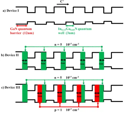
Figures 1(a), 1(b), and 1(c) depict the schematic energy band diagrams of the InGaN/GaN active region for the devices with the undoped quantum barriers, Si step-doped quantum barriers, and PN-doped quantum barriers, respectively. The studied devices were grown on c-sapphire substrates by AIXTRON metal-organic chemical vapor deposition (MOCVD) system. The growth was initiated on c-sapphire substrates [26]. A 30 nm low-temperature nucleation layer was grown prior to a 2 μm u-GaN layer. The doping profile in the subsequent 4 μm thickness n-GaN layer (ND = 5 × 1018 cm3) was achieved through the diluted SiH4, while Cp2Mg was used
for the p-GaN layer (0.2 μm with the Mg dopant concentration of 3 × 1019 cm3). TMGa and NH3 serve as the precursors for the bulk GaN layer. A 20 nm p-Al0.20Ga0.80N layer was inserted
between the five-period InGaN/GaN multiple quantum wells (MQWs) and the p-GaN layer as the electron blocking layer, which was grown under 100 mbar to prevent the parasitic reaction between TMAl and NH3. The width of the In0.15Ga0.85N quantum wells is 3 nm, for which TMIn
and TEGa were used as the group-III reaction precursors. We used a growth temperature of 742 °C and 785 °C for the quantum well and quantum barrier growth, respectively. The three devices only differ from each other in their quantum barrier architecture. Device I is the reference device
with the undoped GaN as the quantum barriers (12 nm), while N-type step-doped quantum barriers [4 nm doped thickness with ND = 5 × 1017 cm3 in Fig. 1(b)] were used in Device II
according to our previous work [25]. Device III is the proposed design with PN-type quantum barriers. In order to suppress the Mg diffusion [27], the quantum barriers are selectively doped by Mg dopants as shown in Fig. 1(c). Specifically, the growth of each PN-type quantum barrier was divided into three steps under the same growth temperature of 742 °C, while the growth pressure was kept to be 305 mbar. We grew undoped GaN region for 4 nm first, then Cp2Mg was
supplied to grow the P-type region of 4 nm thickness. The molar ratio between Cp2Mg and
TEGa was 5.26 × 10⁴. Lastly, the other 4 nm N-type GaN region was grown by closing the Cp2Mg supply and opening SiH4 supply. The thermal annealing to activate Mg dopants for both
PN-type quantum barriers and p-GaN layer was conducted for 600 sec under 730 °C. However, because of the large ionization energy of Mg (~200 meV) and the hydrogen-passivation in the GaN layer, thus, we set the Mg ionization efficiency to 1% in our simulation [28].
GaN quantum
barrier (12nm) Inwell (3nm)0.15Ga0.85N quantum
C+ a) Device I 4nm 4nm 4nm 4nm 4nm n = 5 1017 cm-3 b) Device II 4nm 4nm 4nm 4nm n = 5 1017 cm-3 p = 1 1017 cm-3 c) Device III
Fig. 1. Schematic energy band diagrams of the InGaN/GaN active region for (a) Device I with the undoped quantum barriers, (b) Device II with the Si step-doped quantum barriers and (c) Device III with the PN-type quantum barriers.
The devices are modeled and systematically simulated using APSYS [25], which self-consistently solves the Poisson equations, Schrödinger equations and the continuity equations with the proper boundary conditions. The six-band k·p theory is performed to take account of the carrier screening effect in InGaN quantum wells [29]. The energy band offset ratio between the conduction band and the valence band in the InGaN/GaN quantum well region is set to be 70/30 [30]. In order to consider the crystal relaxation by generating misfit dislocations, only 40% of the theoretical polarization charge density is assumed [31]. We have set the Auger recombination coefficient to be 1 × 1030 cm6/s [32, 33]. The Shockley-Read-Hall (SRH) lifetime for electrons and holes is set to be 43 ns [33]. The Other parameters used in the simulations can be found in the previous work [34].
To verify the theoretical results, InGaN/GaN LED chips were fabricated by a standard fabrication process. The LED mesa (with a chip size of 350 × 350 μm2
) was obtained by reactive ion etch (RIE). Ni/Au (5 nm/5 nm) was deposited by E-beam as the transparent current spreading layer (TCL) on the p-GaN layer. Ti/Au (30 nm/150 nm) was finally deposited on the n-GaN layer and TCL simultaneously for metal contacts.
3. Results and discussion
350 400 450 500 550 0 100 200 300 400 EL In ten sit y (a.u ) Wavelength (nm) (a) 80 A/cm2 16 A/cm2 350 400 450 500 550 (b) Wavelength (nm) 80 A/cm2 16 A/cm2 350 400 450 500 550 80 A/cm2 (c) Wavelength (nm) 16 A/cm2
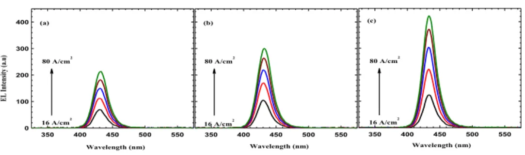
Fig. 2. Experimentally measured EL spectra for (a) Device I, (b) Device II and (c) Device III at 16, 32, 48, 64 and 80 A/cm2, respectively.
Figures 2(a), 2(b) and 2(c) show the experimentally measured electroluminescence (EL) spectra at various current density levels for Devices I, II and III, respectively. Among the three devices, the strongest EL intensity is observed from Device III with the PN-type quantum barriers. The strong EL intensity is attributed to the improved hole transport across the active region with the introduction of Mg dopants. In addition, the screening of the QCSE by Si step-doping the quantum barriers has also increased the radiative recombination rates in the quantum wells, resulting in a better device performance.
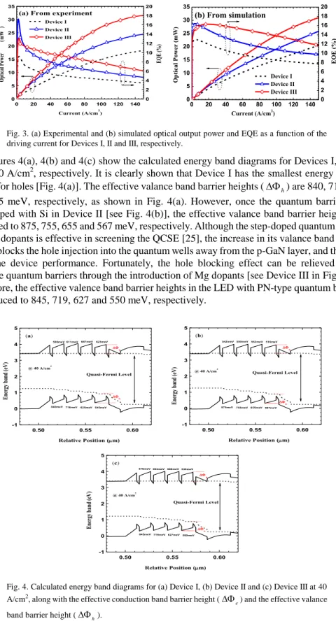
The experimentally measured optical output power and external quantum efficiency (EQE) for Devices I, II and III are shown in Fig. 3(a). Consistently with the simulated results shown in Fig. 3(b), Device II and Device III emit more optical power than Device I with Device III being the strongest. For example, the optical power measured for Devices I, II and III at 150 A/cm2 is 18.29, 24.50, and 31.65 mW, respectively in Fig. 3(a). This translates to a power enhancement of 33.95% and 73.05% for Device II and Device III, respectively, compared to Device I. The simulated optical output power and EQE for Devices I, II and III are shown in Fig. 3(b) which are in excellent agreement with the experimental results in Fig. 3(a). The simulated results provide us an insightful understanding on the improvement of the optical power and EQE of the proposed device. It is found that the screening effect of the QCSE by the Si-doped quantum barriers is responsible for the improvement observed in Device II [25] and partially responsible for Device III. The further improvement in Device III comes from the hole transport promotion by Mg doping the quantum barriers. Through the application of the PN-type quantum barriers, the energy band structure, hole distribution across the active region, and the electric field profile have been modified and become favorable for the improvement of the optical output power and EQE, which will be shown in detail subsequently. It should be noted that although the experimental and simulated results are generally in excellent agreement, there still exist some discrepancies in the absolute values and trending details at the low current density levels. These are due to the uncertainties in the temperature dependence of the parameters used in simulation such as the Auger recombination coefficient, the SRH recombination coefficient and the thermal conductivity of the compounds as well as the experimental error at the low current density levels.
0 20 40 60 80 100 120 140 0 5 10 15 20 25 30 35 EQ E ( % ) Op tical Powe r (mW ) Current (A/cm2 ) Device I Device II Device III 0 2 4 6 8 10 12 14 16 18 20
(a) From experiment
0 20 40 60 80 100 120 140 0 5 10 15 20 25 30 35 EQ E (% ) O pt ical Powe r (m W ) Current (A/cm2) Device I Device II Device III 0 2 4 6 8 10 12 14 16 18 20 (b) From simulation
Fig. 3. (a) Experimental and (b) simulated optical output power and EQE as a function of the driving current for Devices I, II and III, respectively.
Figures 4(a), 4(b) and 4(c) show the calculated energy band diagrams for Devices I, II and III at 40 A/cm2, respectively. It is clearly shown that Device I has the smallest energy barrier height for holes [Fig. 4(a)]. The effective valance band barrier heights (h) are 840, 716, 625 and 545 meV, respectively, as shown in Fig. 4(a). However, once the quantum barriers are step-doped with Si in Device II [see Fig. 4(b)], the effective valance band barrier heights are increased to 875, 755, 655 and 567 meV, respectively. Although the step-doped quantum barrier with Si dopants is effective in screening the QCSE [25], the increase in its valance band barrier height blocks the hole injection into the quantum wells away from the p-GaN layer, and this may limit the device performance. Fortunately, the hole blocking effect can be relieved in the PN-type quantum barriers through the introduction of Mg dopants [see Device III in Fig. 4(c)]. Therefore, the effective valence band barrier heights in the LED with PN-type quantum barriers are reduced to 845, 719, 627 and 550 meV, respectively.
0.50 0.55 0.60 -1 0 1 2 3 4 5 Quasi-Fermi Level @ 40 A/cm2 Relative Position (m) En er gy b an d ( eV) (a) 545meV 625meV 716meV 840meV 623meV 687meV 611meV 598meV h e 0.50 0.55 0.60 -1 0 1 2 3 4 5 (b) 516meV 553meV 550meV 542meV 567meV 655meV 755meV Quasi-Fermi Level @ 40 A/cm2 Relative Position (m) En er gy b an d ( eV) 875meV h e 0.50 0.55 0.60 -1 0 1 2 3 4 5 (c) Quasi-Fermi Level @ 40 A/cm2 Relative Position (m) En er gy b an d ( eV) 550meV 627meV 719meV 845meV 536meV 588meV 593meV 576meV h e
Fig. 4. Calculated energy band diagrams for (a) Device I, (b) Device II and (c) Device III at 40 A/cm2, along with the effective conduction band barrier height (e) and the effective valance
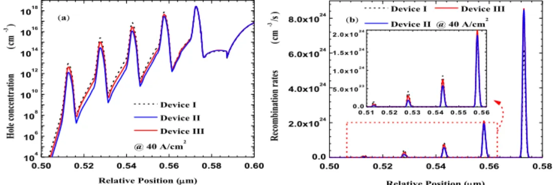
In order to reveal the hole transport for Devices I, II and III with various quantum barrier schemes, we have further simulated the hole distribution across the quantum wells, as shown in Fig. 5(a). Comparatively, we can see that Device I shows the most homogenous hole distribution across the active region because of the undoped GaN quantum barriers. On the other hand, for Device II, the holes have difficulty to penetrate across the active region due to its increased valence band barrier heights. As for Device III, since the valance band barrier heights are reduced through introducing Mg in the quantum barriers, holes are better distributed compared to Device II. However, since the ionized Mg in the quantum barriers is assumed to be 1 × 1017 cm3 in our simulation, which is still smaller than the Si doping concentration, thus the valance band barrier height in Device III is still larger than that in Device I, and we still observe a less homogenous hole distribution if compared to Device I. Nevertheless, one can also properly reduce the quantum barrier thickness of Device III for an even better hole transport. Separately, we have examined the radiative recombination rates in each quantum well for Devices I, II and III numerically, as shown in Fig. 5(b). Although Devices I, II and III have the identical hole concentration in the quantum well that is closest to the p-GaN layer, the excellent screening of the QCSE with the Si-doped quantum barriers facilitates the strongest radiative recombination rates in the last quantum well for both Devices II and III [25]. Therefore, the enhanced overall radiative recombination rates and optical output power have been obtained in Figs. 3(a) and 3(b), respectively. For the rest of the quantum wells that are away from the p-GaN layer, Device III has the better radiative recombination rates compared to Device II due to the reduced valance band barrier height by selectively doping Mg in the quantum barriers, and this translates to the strongest optical output power for Device III according to Figs. 3(a) and 3(b), respectively.
0.50 0.52 0.54 0.56 0.58 0.0 2.0x1024 4.0x1024 6.0x1024 8.0x1024 0.51 0.52 0.53 0.54 0.55 0.56 0.0 5.0x10² 3 1.0x10² 4 1.5x10² 4 2.0x10² 4 (b)
Device I Device III Device II @ 40 A/cm2 Relative Position (m) Re com binat ion r ate s (cm -3 /s) 0.50 0.52 0.54 0.56 0.58 0.60 104 106 108 1010 1012 1014 1016 1018 (a) Device I Device II Device III @ 40 A/cm2 Hole c on ce nt ration (cm -3) Relative Position (m)
Fig. 5. Simulated (a) hole concentration and (b) the radiative recombination rates for Devices I, II and III, respectively.
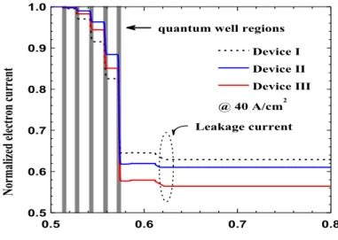
The leakage current is shown in Fig. 6. We have seen that the leakage current is 62.9%, 61.0% and 56.4% for Devices I, II and III, respectively. The suppressed leakage current in Devices II and III compared to Device I is attributed to the increased overall radiative recombination rates in the active region [see Fig. 5(b)] [30]. On the other hand, by introducing Mg dopants in the quantum barriers, the effective conduction band barrier height (e) can be increased for Device III when compared to Device II [see ein Figs. 4(b) and 4(c)]. Thus, an even better electron confinement in Device III is obtained once the effective conduction band barrier height is increased [10, 12], and this can further reduce the electron leakage current according to Fig. 6.
0.5 0.6 0.7 0.8 0.5 0.6 0.7 0.8 0.9 1.0
quantum well regions Device I Device II Device III @ 40 A/cm2 Relative Position (m) Nor mali ze d e lec tron cu rr en t Leakage current
Fig. 6. Simulated leakage current for Devices I, II and III, respectively.
0 1 2 3 4 5 6 7 0 10 20 30 40 50 60 70 80
(a) From experiment
Cu rr en t (A/c m 2 ) Voltage (V) Device I Device II Device III 0 1 2 3 4 5 6 7 0 10 20 30 40 50 60 70 80 (b) From simulation Cu rr en t ( A/c m 2 ) Voltage (V) Device I Device II Device III
Fig. 7. (a) Experimentally measured and (b) simulated current as a function of the applied voltage for Devices I, II and III, respectively.
The measured and simulated current as a function of the applied bias for the LED chips are demonstrated in Figs. 7(a) and 7(b), respectively. It can be seen from Figs. 7(a) and 7(b) that Devices II and III exhibit a substantial improvement in their electrical performance compared to Device I. The enhanced on-state current is due to the improved electron transport in Devices II and III both with Si-doped quantum barriers. The Mg-doping in the quantum barriers for Device III also helps to enhance the hole injection and thus Device III has a slightly better electrical performance than Device II both from experiment and simulation. Furthermore, the strong radiative recombination current helps for a better electrical conductivity.
0.565 0.570 0.575 0.580 0.585 -7x10⁵
-6x10⁵ 2.0x10⁵
4.0x10⁵
the electric field profile in QB
the electric field profile in QW Device I Device II Device III Relative Position (m) Elec tric f ield (V/c m) C+ (a) 0.572 0.573 0.574 0.575 0.0 0.2 0.4 0.6 0.8 1.0 (b) Device I Device II Device III Electron wave function Relative Position (m) Nor mali zed car rier wave fu nc
tions Hole wave function
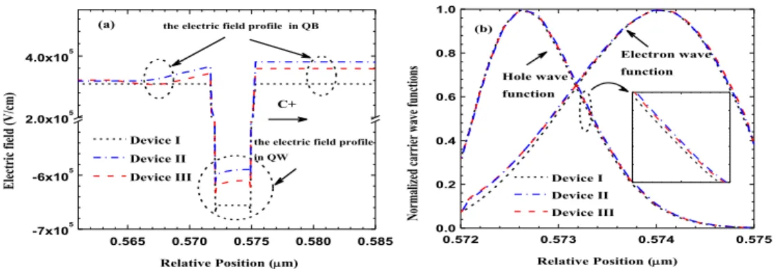
Fig. 8. (a) Electric field profile under equilibrium and (b) distribution of the electron and hole wave functions in the quantum well closest to the p-GaN layer for Devices I, II, and III, respectively. The positive direction of the electric field in (a) is along the growth orientation, i.e., C+-orientation.
According to Fig. 5(b), the quantum well closest to the p-GaN layer contributes most to the radiative recombination, and thus it is worth studying the electric field within it through the theoretical simulation. We have shown the electric field profile for the last quantum barrier (QB)-quantum well (QW) pair under the equilibrium in Fig. 8(a). It can be seen that the electric field within the QW is reduced in both Devices II and III compared to Device I. The reduced electric field in the QW is due to the screening effect of the QCSE by the ionized Si dopants and the electrons diffusing into the QW, as has been reported by our previous work [25]. The QW electric field in Device III is slightly larger than that in Device II, which is due to the Mg compensation effect to the Si dopants in the quantum barrier. The carrier wave functions at 40 A/cm2 are demonstrated in Fig. 8(b) for Devices I, II and III, respectively. As has been reported in our previous work [25], a reduced electric field in the quantum well enhances the electron-hole overlap level (Гe-hh). Hence, the calculated Гe-hh is 30.83%, 33.13% and 32.87% in
Fig. 8(b) for Devices I, II and III, respectively. It can be seen that PN-type quantum barrier is less effective in screening QCSE if compared to Si-step-doped quantum barrier. Nevertheless, the improved hole transport promotes the radiative recombination and thus the optical power and EQE have been significantly enhanced. It should be noted that the existence of the Mg-Si-doped quantum barrier as shown in Device III will gives rise to a built-in PN-junction which is reversely biased when the device is forwardly operated. However, this reversely biased PN-junction will not result in a large electrical resistance, since the ionized Mg dopants in the quantum barriers is 1 × 1017 cm3 with a 4 nm thickness while the Si doping concentration is 5 × 1017 cm3 with a 4 nm thickness, and hence the P-doped region in the quantum barriers is fully depleted and the quantum barriers will be in a reach-through mode [35]. As a result, any increased bias can promote a high current flow.
Besides, it is noteworthy that we have utilized four PN-type quantum barriers in this work, however, the number of PN-type quantum barriers and the Mg-doped position in each quantum barrier can be further optimized. By doing so, the possible Mg diffusion from the PN-type quantum barriers into the quantum wells can be further suppressed. Meanwhile, considering the compensation effect to the Si-doped position by those diffused Mg dopants in each quantum barrier, the Si dosage and Si-doped thickness can also be properly increased.
4. Conclusions
In conclusion, the InGaN/GaN LED with PN-type quantum barriers is proposed and investigated both numerically and experimentally in this work. Substantial enhancement of the optical output power has been achieved, which is due to the screening of the QCSE by Si doping
and the promoted hole transport across the multiple quantum wells. The PN-type quantum barrier is favorable for the more homogenous distribution of holes and radiative recombination rates across the whole active region in the proposed device, yielding a better LED performance. In addition, the increased effective conduction band barrier height in the proposed PN-type quantum barriers further suppresses the electron overflow, which further improves the LED performance. As a result, the proposed PN-type quantum barriers theoretically and experimentally prove to be very promising for high-performance LEDs.
Acknowledgments
This work is supported by the National Research Foundation of Singapore under Grant No. NRF-CRP-6-2010-2 and NRF-RF-2009-09 and the Singapore Agency for Science, Technology and Research (A*STAR) SERC under Grant No. 112 120 2009. The work is also supported by the National Natural Science Foundation of China (NSFC) (Project Nos. 61006037, 61177014 and 61076015).