⊥Department of Electrical and Computer Engineering, University of Toronto, 10 King’s College Road, Toronto, Ontario M5S 3G4, Canada
¶Institute of Applied Physics and Materials Engineering, University of Macau, Macao SAR 999078, China #China Academy of Engineering Physics, Mianyang 621900, China
∝MajuLab, CNRS-UCA-SU-NUS-NTU International Joint Research Unit, UMI 3654, Singapore
∥Department of Electrical and Electronics Engineering, Department of Physics, UNAM−Institute of Materials Science and Nanotechnology, Bilkent University, Ankara 06800, Turkey
*
S Supporting InformationABSTRACT: Lead-halide perovskites have been attracting attention for potential use in solid-state lighting. Following the footsteps of solar cells, the field of perovskite light-emitting diodes (PeLEDs) has been growing rapidly. Their application prospects in lighting, however, remain still uncertain due to a variety of shortcomings in device performance including their limited levels of luminous efficiency achievable thus far. Here we show high-efficiency PeLEDs based on colloidal perovskite nanocrystals (PeNCs) synthesized at room temperature possessing dominant first-order excitonic radiation (enabling a photoluminescence quantum yield of 71% in solidfilm), unlike in the case of bulk perovskites with slow electron−hole bimolecular radiative recombination (a second-order process). In these PeLEDs, by reaching charge balance in the recombination zone, wefind that the Auger nonradiative recombination, with its significant role in emission quenching, is effectively suppressed in low
driving current density range. In consequence, these devices reach a maximum external quantum efficiency of 12.9% and a power efficiency of 30.3 lm W−1at luminance levels above 1000 cd m−2as required for various applications. Thesefindings suggest that, with feasible levels of device performance, the PeNCs hold great promise for their use in LED lighting and displays.
KEYWORDS: Colloidal nanocrystal, lead-halide perovskite, light-emitting diodes
L
ead-halide perovskites with direct band gaps have emerged as a new material system for low-cost, large-area, and lightweight optoelectronics.1−21 Previous reports have con-firmed promising performance for this material family in light generation.13−21With binding energy up to dozens of meV and long electron−hole diffusion length of micrometers at room temperature, carriers are almost free and delocalized in bulk perovskites16,22−24 leading to slow electron−hole bimolecular radiative recombination (a second-order process).11,24 Com-peting with trap-mediated nonradiative decay (a first-order process), this radiation process limits the efficiency levels.11,24Recently a strategy that enhances the photoluminescence quantum yield (PLQY) of light emitters and external quantum
efficiency (EQE) of their LEDs has been developed by
localizing the charge carriers in small sized lead-halide perovskite grains or quantum wells.16−21However, even though such colloidal perovskite nanoparticles can present PLQY of near unity in solution and above 60% infilm, their performance levels have been still severely limited during the device operation to date.19,20,25,26 Therefore, deeper understanding of device performance limits and a new way divorced from this low performance are required. Here we present highly efficient PeLEDs based on colloidal CH3NH3PbBr3(MAPbBr3) PeNCs
with efficient first-order excitonic radiation reaching a 71% PLQY in film. Because of the significant role of Auger Received: February 25, 2018
nonradiative recombination, highly efficient emission at low charge densities is desired. By effectively suppressing Auger nonradiative recombination with balanced charge at low driving charge density levels, these PeLEDs exhibit a high EQE of 12.9% and a high power efficiency level of 30.3 lm W−1at high brightness level above 1000 cd m−2, which indicates the feasibility of colloidal PeNCs in LED applications in terms of efficiency requirements.
Luminescence Dynamics of Lead-Halide Perovskite Emitters. The radiation of bulk perovskites originates from slow bimolecular recombination. The Langevin theory predicts that this bimolecular recombination rate could be four orders of magnitude higher in perovskites, which is one of the main merits ensuring superior performance in photovol-taics.11,24,27−30 The carrier kinetics in bulk lead-halide perov-skites can be described by
= − − − n t t G nk n k n k d ( ) d 1 2 2 3 3 (1)
where n is the carrier density, t is the time, G is the generation rate of carrier density, k1 is the first-order trap-mediated
monomolecular recombination rate constant, k2 is the electron−hole bimolecular recombination rate constant, and
k3 is the many-body Auger recombination rate
con-stant.11,24,27−30 Thus, under steady-state electric excitation, the luminous QY (A(n)) is given by
= + + A n nk k nk n k ( ) 2 1 2 2 3 (2)
The emission efficiency (Figure 1a) first increases with increasing n due to the domination of bimolecular recombina-tion over the trap-mediated nonradiative recombinarecombina-tion. However, at high carrier densities, where the Auger recombination dominates over the bimolecular recombination, the emission efficiency will decrease with increasing n. Since k2 (∼10−10 cm3 s−1) and k3 (∼10−28 cm6 s−1) are the intrinsic
parameters of the bulk perovskites,11,24,27−30 the emission efficiency strongly depends on k1 and n. By ignoring other
quenching factors, with a typical reported value of k1(∼107s−1,
100 ns), the internal efficiency of the PeLEDs is constrained to <10%, even when driving at a high carrier density of 1016cm−3
(Figure 1a).
The bulk perovskitefilms have shown a long carrier lifetime (i.e., low trap states density)31and a high mobility.32Thus, the delocalized charge carriers are also possible to transport through the thin active layer without recombination. When the PeLEDs are driven at a lower carrier density level or under a higher trap density regime (trap-related recombination time <100 ns), the nonradiative recombination could always dominate over the bimolecular recombination, which also leads to an internal QY of <10%. Therefore, the slow bimolecular recombination rate in bulk perovskites limit the PeLEDs working at a relatively low carrier density. The quadratic power dependence of the recombination rate on the carrier densities of MAPbBr3 bulk crystal (Figure 1b) confirms the bimolecular recombination in the bulk perovskite. The experimentally measured curves match well with the theoretical prediction at the low charge carrier density level (Figure 1a,c). It is noted that thefirst-order excitonic emission could compete effectively with the trap-mediated nonradiative recombination in the low carrier density range of n ≤ 1016 cm−3 with trap states density (k1≈ 107s−1) as shown inFigure 1a. Therefore,
small-size PeNCs can enhance the radiative excitonic recombination with increased exciton confinement and exciton binding energy compared to bulk crystals with dominating free-carrier recombination.28Moreover, the surrounded passivation of ligands can decrease the surface defects of PeNCs, which also leads to an increment of QY at low excitation density level.
Synthesis of PeNCs and Their Luminescence Dynam-ics. The colloidal MAPbBr3PeNCs were synthesized by using
antisolvent precipitation method at room temperature. The as-synthesized solution was preaged for 6 days before being used for LEDs fabrication. In this duration, the absorption edge and PL peak gradually red-shift until after 6 days, and the full-width-at-half-maximum (fwhm) of PL spectra keeps narrowing synchronously (Figure 1d, Supplementary Figure 1). Notably,
Figure 1.(a) Calculated injected carrier density dependence of luminescence quantum yield for excitonic emission (k1nr= 107s−1, k1r= 108s−1, k3nr
= 10−26cm6s−1) and bimolecular emission (k1nr= 107s−1, k2r= 10−10cm3s−1, k3nr= 10−28cm6s−1) in different dimensional CH3NH3PbBr3emitters.
(b) Photon-injected charge carrier density dependence of the initial time PL intensity (IPL(t = 0)). The quadratic behavior IPL[t = 0] confirms the
bimolecular recombination in bulk perovskite. (c) Relative PLQY as a function of the photon-injected charge carrier density. (d) PL spectra of colloidal PeNCs solution aging for 6 days. Peak emission wavelengths redshift: 506.5, 512.5, 514.6, 516.4, 517.8, 518.5 nm. The fwhm decreases: 32.7, 25.7, 24.9, 24.8, 24.7, 24.7 nm. (e) XRD pattern migration of PeNCs in 6 days. (f) TEM and high-resolution TEM image of the as-synthesized PeNCs. Scale bars: 50 and 2 nm. d (200) = 2.93 Å, d (210) = 2.65 Å.
the PLQY was significantly enhanced from 70% in solution and 35% infilm to 89% in solution and 71% in film. From nuclear magnetic resonance (NMR), the composition of the MAPbBr3
NCs was found to remain stable during the aging time (Supplementary Table 1). However, as observed in X-ray diffraction (XRD) patterns, the MAPbBr3NCs show increased crystallization during this process (Figure 1e). The high-resolution transmission electron microscopy (HR-TEM) measurements (Figure 1f) illustrate that the aged PeNCs still exhibit a small crystal size (<8 nm). The lattice fringes of the MAPbBr3PeNCs are 2.93 and 2.65 Å, which correspond to the
(200) and (210) facets of the cubic phase MAPbBr3,
respectively. With the passivation of ligands and solvent molecules, the low-crystallinity MAPbBr3 NCs in colloidal
solution possess a high PLQY. However, the passivation effect decreases drastically infilm (Supplementary Table 1); thus, the defect sites become significant in quenching emission through the competition with radiation process. Though with similar passivation, the highly crystallized NCs with a low defect sites display low trap-assisted nonradiative recombination, which ensures a high PLQY infilm. Even with such passivation effects, the PeNCs still show high mobility of 0.22 cm2 V−1 s−1 for holes and 0.48 cm2V−1s−1for electrons (Supplementary Figure 2).
As illustrated inFigure 1b, for MAPbBr3PeNCs, IPL[t = 0] is
nearly linearly dependent on the carrier density from 5× 10¹⁴ to 2× 1017cm−3, which suggests that the emission is mainly
from thefirst-order excitonic radiation process,27in agreement with a recent report in formamidinium lead halide nanocryst-als.28 Below 5 × 1014 cm−3, the trap-mediated nonradiative
recombination dominates over the excitonic emission. Above 2 × 1017 cm−3, the multiparticle Auger recombination prevails.
Therefore, MAPbBr3PeNCs feature a high PLQY level under the charge carrier density from 1015 to 1016 cm−3, which matches well with the device working regime in PeLEDs (Figure 1c).27 Therefore, the highly efficient first-order excitonic emission suggests the MAPbBr3 PeNCs as suitable
candidates for efficient PeLEDs.
Investigation of PeLEDs. As the top most important parameter for EL device characterization, EQE, which is defined
as the number of emitted photons per injected electrons, is given as the product of four different parameters:
=E ×E ×E ×E
EQE in s/t rad out (3)
Therein the first parameter Ein indicates the charge balance
factor in recombination zone. The second one Es/t gives the fraction of excitons that are allowed to radiate by spin statistics. The third factor Erad depicts the fraction of the intrinsic radiative efficiency of the emitter. The last one Eoutdetermines
the photon extraction efficiency in a device. In this work with the proposed devices using normal structure without any additional measurement for spin injection of charge carriers or enhanced outcoupling efficiency of radiation, thus, all attention was paid onto the charge balance factor in recombination zone to reach the high device efficiency promised by MAPbBr3
PeNCs. Moreover, because of the significant role of Auger nonradiative recombination (Figure 1a,c), which is to be effectively suppressed in the proposed MAPbBr3 PeNCs devices, a high EQE in low driving current density level was also targeted. In addition to EQE, the power efficiency, especially at high brightness level, is also a critical parameter for evaluating the potential applications of LEDs; therefore, a low driving voltage is essential.
To obtain high quality PeNCsfilm, a classical PEDOT:PSS layer was selected as hole injection/transport layer (HIL/HTL) for all devices in this work (Figure 2a,b and Supplementary Figures 3 and 4). As a good HIL/HTL, PEODT:PSS may lead to emission quenching of PeNCs at HTL/PeNCs interface, but we did not observe a significant weakness of emission comparing to the PeNCs film deposited onto other polymer substrates, like poly-TPD, at an excitation wavelength of 365 nm. The insertion of an insulating thinfilm can improve charge balance by blocking the majority carriers, but this would probably be accompanied by high driving voltage, which would lead to high power consumption and low power efficiency.
To balance the injected hole, a blended layer of B3PYMPM:TPBi (1:X w/w) with adjustable electron transport capability by changing the ratio of two components served as an electron transport layer (ETL) (Figure 2a,b). The deeper LUMO level (−3.4 eV) and high electron conductivity (4.1 × 10⁻⁷S cm−1) of B3PYMPM can lower down the barrier for
Figure 2.(a) Device structure with energy level alignment. (b) SEM of device cross-section showing the multilayer structure with distinct contrast. Scale bar: 100 nm. (c) I−V curves of electron single carrier devices with different electron transport layers. (d) Normalized PL spectrum of PeNCs film and normalized EL spectra of champion PeLEDs at different brightness levels from 500 to 15 000 cd m−2around. The peak emission wavelength
effective electron injection and transport with low driving voltage.20,33,34 Because of the significant difference of the electron conductivity in TPBi and B3PYMPM,33the electron transport capability of the blended ETL can be tuned in a large range (Figure 2c). According to Miller−Abrahams hopping
model, electrons transport through a hopping process between the localized occupied and unoccupied state. In the blended ETL, TPBi (B3PYMPM) molecules play the role of an energy barrier (trap) to scatter the electron transfer between two B3PYMPM (TPBi) molecules, leading to a tunable electron transport capability.35 In the single carrier device with TPBi ETL, as the low electron conductivity (4.2× 10⁻¹⁰S cm−1) and high energy barrier for electron injection caused by the high lying LUMO level of TPBi, the driving voltage is much higher than that of single carrier device with B3PYMPM ETL, which can offer a much higher level of electron conductivity and a deeper LUMO level (Figure 2a,c).33,34 For the single carrier device with B3PYMPM:TPBi (1:X, w/w) ETL, the blended layer shows a tunable electron transport capability depending on the varied component ratio (Figure 2c). To reach a high
power efficiency, a n-type doped electron injection layer was used for a low driving voltage.20
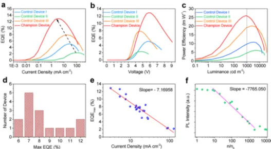
Control device I with pure TPBi ETL and control device II with pure B3PYMPM ETL were selected as the baseline. As seen inFigure 2d, PeLEDs show a green color emission with a nearly ideal Lambertian profile (Supplementary Figure 5). Control device I exhibits overall performance of 15 130 cd m−2 in Lmax, 5.11% in EQEmax, and 10.82 lm W−1inηmax(Figures 2,
3,Table 1, and Supplementary Table 2). On the other hand, control device II displays a higher Lmaxof 24 410 cd m−2and a drastically decreased driving voltage, but a lowerηmaxof 5.96 lm
W−1caused by a lower EQEmax of 2.39% compared to control
device I (Table 1andFigures 2and3). With B3PYMPM:TPBi (1:2, w/w) ETL, control device III shows the best overall performance up to now, with Lmaxof 33 570 cd m−2, EQEmaxof
7.91%, andηmaxof 20.18 lm W−1(Figures 2and3,Table 1, and
Supplementary Table 3). In all devices, the influence of Es/t,
Erad, and Eout can be neglected because the emitters are identical, and the difference in refractive index between TPBi and B3PYMPM is also negligible. Therefore, the significant
Figure 3. (a) EQE-current density characteristics. (b) EQE−voltage dependences. (c) Power efficiency−luminance correlations. (d) EQEmax
histogram for 15 champion devices from four batches. (e) Dependencies between EQEmaxand the corresponding driving current density (scatters,
experiment result; solid line, simulation by linearfitting). (f) PL intensity of MAPbBr3 layer in an electron single carrier device; no. is the density of electron injected into PeNCs layer when the current density is 1.0× 10⁻²mA cm−2(scatters, experiment result; solid line, simulation by linear fitting).
Table 1. Key Parameter Comparison of PeLEDsa
device structure Von (V) Lmax (cd m−2) EQEmax (%) (lm Wηmax−1) control device I
ITO/PEDOT:PSS (40 nm)/MAPbBr3PeNCs (40 nm)/TPBi (30 nm)/TPBi: Cs2CO3(10:1 w/w, 20 nm)/Al (100 nm). 3.3 15 130 5.11 10.82 3.4 16 470 5.06 7.03 3.6 14 190 4.81 7.49 control device II
ITO/PEDOT:PSS (40 nm)/MAPbBr3PeNCs (40 nm)/B3PYMPM (30 nm)/B3PYMPM: Cs2CO3(10:1 w/w, 20 nm)/Al (100 nm). 2.7 24 410 2.39 5.96 2.6 23 290 2.28 6.21 2.7 23 120 2.19 5.62 control device III
ITO/PEDOT:PSS (40 nm)/MAPbBr3PeNCs (40 nm)/B3PYMPM:TPBi (1:2 w/w, 30 nm)/ B3PYMPM: Cs2CO3(10:1 w/w, 20 nm)/Al (100 nm). 3.0 33 570 7.91 20.18 2.9 30 380 6.75 17.92 3.0 32 730 7.25 18.47 champion device
ITO/PEDOT:PSS (40 nm)/ MAPbBr3PeNCs (80 nm)/B3PYMPM:TPBi (1:2 w/w, 30 nm)/ B3PYMPM: Cs2CO3(10:1 w/w, 20 nm)/Al (100 nm).
3.1 22 830 12.9 26.07 3.0 43 400 7.53 17.56 2.9 25 410 10.67 30.3 aV
on, turn on voltage @ 1 cd m−2; Lmax, maximum luminance; EQEmax, maximum external quantum efficiency; ηmax, maximum power efficiency.
hole into ETL as the maximum effective radius of Förster energy transfer is 6 nm. It was thus deducted that hole is the major charge carrier in the recombination zone of control device I (Supplementary Figure 6). Otherwise, the pure PeNCs green color emission in Ir(piq)2acac indicator device with
B3PYMPM ETL would have suggested there was less or no hole injection into ETL compared to TPBi devices ( Supple-mentary Figure 6). With the same hole injection, the highest EQEmaxsuggested the best charge balance in control device III
with medium electron supply ETL comparing to I and II (Figure 2,3). Therefore, the lowest EQEmaxof control device II was ascribed to the overwhelming majority of electrons in the PeNCs emissive layer as the highest electron supply of B3PYMPM.
In amorphous organic semiconductor, the LUMO/HOMO level distribution was broad, of which the tail extended into the band gap as gap states.36 Moreover, as σ = neμe (where σ is
electron conductivity, n is the electron concentration, e is the elementary charge, μe is the electron mobility) indicates, a
comparable electron mobility but significantly high electron conductivity suggest high electron concentration. Thus, here it was deducted that the amount of gap sates in B3PYMPM is much higher comparing to TPBi, which can be supported by the smaller distance between the Fermi level and LUMO level of B3PYMPM comparing to TPBi (Supplementary Figure 7). In consequence, with a deeper LUMO level, there were more electrons injected into B3PYMPM layer even when the applied bias was less than the threshold voltage of 2.2 V compared to TPBi (Figure 2e). By the law of charge conservation, in a closed-loop circuit, the electrons injected into B3PYMPM layer will transit to the valence band of PeNCs by a nonradiative process, leading to leakage current (Figure 2a,e). Moreover, under high driving voltage, the excessive electrons injected into the conductive band of PeNCs will transit to the Fermi level of PEDOT:PSS by a nonradiative process as current overflow, which is another way of leakage current for control device II working in high driving current density range. The leakage of carriers that flow through the device without recombining drives down the EQE directly. Moreover, the imbalanced charge also leads to an enhanced Auger nonradiative recombination. Thus, control device II presented the lowest EQEmax among all devices. As exhibited in Figure 2e, with
blended ETL, the leakage current density was suppressed significantly by 3−4 magnitudes. In most practical LEDs, such leakage current was ascribed to device inherent structure. Therefore, we believe that, in control device III by decreasing the amount of electron injected into the recombination zone
max
batches describes the distribution of EQEmax of the fabricated
PeLEDs (Figure 3d). Because of the significant difference
between CB and THF colloidal solution in PeNCs film
deposition (Supplementary Figures 8 and 9), the reproduci-bility of PeNCsfilm deposition using THF:CB (Y:1 v/v, Y = 16) colloidal solution is moderate. To balance the EQEmaxand Lmax, the peak value of 43 440 cd m−2in Lmax, 12.9% in EQE,
and 30.3 lm W−1in η (at a luminance level of 2069 cd m−2, which meets the requirement for lighting application of 1000 cd m−2) were observed from different champion devices (Table 1,
Figure 3). Furthermore, we measured the device half-lifetime to be around 6 min (Supplementary Figure 10), which is still a daunting problem for PeLEDs, and there is a considerable margin to improve. Moreover, with the same device structure except a slightly changed ratio of B3PYMPM:TPBi (1:1.5, w/ w), a PeLEDs with emitter of CsPbBr3nanocrystals also offered
a high performances, including a EQEmax of 12.4%, for which
details will be discussed in the following work.
For all devices, it was found that a higher EQEmax
corresponds to a lower driving current density (Jc) (Figure 3a,e). As the device structures were different, the exponential dependence was probably related to the luminescence dynamics of PeNCs. The rising of driving current density EQEs increases from very low initial values (Figure 3a), which is caused by the competition of traps. Additionally, because of the high carrier mobilities of PeNCs holes and electrons meet and recombine with low probability, which is also a reason for the negligible EQE value in the low driving current density. With the increasing driving current density, the radiative excitonic recombination takes a dominating role gradually. With the further increase of the driving current density, the Auger nonradiative recombination dominates over the excitonic recombination. However, the imbalanced charges in the recombination zone, which do not exist in the photoexcitation process, boosts the nonradiative Auger process even at the low driving current density level (Figure 3a,f). As shown by the electron single carrier PeNCs device, the excessive electrons injected into the PeNCs layer lead to a significantly quenched PL even at a low electron density (n) level. Though the charge balance factors are the same in the recombination zone for control device III and champion device, the thicker emissive layer of champion device can decrease the charge density, allowing for a weak Auger nonradiative recombination compared to control device III.
Conclusion. In summary, we have demonstrated highly efficient PeLEDs using colloidal organometal halide PeNCs. The high-quality colloidal MAPbBr3PeNCs with efficient
one-order excitonic emission were synthesized at room temperature. As the significant Auger nonradiative recombination caused by high driving current density and imbalanced charge, the PeLEDs with optimized charge balance in low driving current density level were developed and reached an EQEmaxof 12.9%
accompanied by high ηmax of 30.4 lm W−1at high brightness above 1000 cd m−2. This work demonstrates a breakthrough advancement toward the ultimate goal of application of PeLEDs and lays down a systematic constructive approach for researchers on halide PeLEDs in their future works.
Methods. Materials and Chemicals. Methylamine (MA) solution in ethanol, formamidine acetate, hydrobromic acid (HBr), hydroiodic acid (HI), lead bromide (PbBr2), lead iodide (PbI2), octylamine, anhydrous N,N-dimethylformamide
(DMF), γ-butyrolactone, tetrahydrofuran (THF), and chlor-obenzene (CB) were all purchased from Sigma-Aldrich. PEDOT:PSS (AI 4083) was purchased from Heraeus. 1,3,5-Tris(N-phenylbenzimiazole-2-yl)benzene (TPBi), cesium car-bonate (Cs2CO3),
4,6bis(3,5di(pyridin3yl)phenyl)2methy l p 4,6bis(3,5di(pyridin3yl)phenyl)2methy r i m i d i n e ( B 3 P Y M P M ) , ) , p o l 4,6bis(3,5di(pyridin3yl)phenyl)2methy ( 4 b u t 4,6bis(3,5di(pyridin3yl)phenyl)2methy l p h e n 4,6bis(3,5di(pyridin3yl)phenyl)2methy l -diphenylamine) (poly-TPD), and bis(1-phenylisoquinoline)-(acetylacetonate)iridium(III) (Ir(piq)2(acac)) were purchased from Lumtec. The colloidal zinc oxide (ZnO) nanoparticles (N-11) were purchased from Avantama. All chemicals were used as received.
Lead-Halide Perovskite Preparation. MABr. CH3NH2
solution in ethanol was reacted with HBr in water with excess methylamine at 0 °C. The precipitate was recovered via evaporation at 60°C. The yellowish raw product was washed with diethyl ether five times and dried at 60 °C in a vacuum oven for 24 h.
MAPbBr3 PeNCs. Samples of 0.225 mmol MABr and 0.15
mmol PbBr2were dissolved in 0.5 mL of anhydrous DMF and
8.5 mL of γ-butyrolactone mixed solution with 15 μL of octylamine to form a halide perovskite precursor solution. A 0.3 mL sample of the perovskite precursor solution was dropped into 5 mL of toluene with vigorous stirring. The colloidal solution was stored in sealed vial for 1 week before use. After aging 1 week, we can get the perovskite NCs with higher PLQY. Then the colloidal solution was centrifuged at 5000 rpm for 5 min to discard the aggregated precipitates, and the PeNCs were obtained after being centrifuged at 14 800 rpm. The PeNCs product was dispersed in solvent to form the colloidal solution with 5 mg/mL concentration for LEDs fabrication.
MAPbBr3 Bulk Crystal. The 1 mmol MABr and 1 mmol
PbBr2 were dissolved in 0.5 mL of DMF and 0.5 mL of
γ-butyrolactone mixed solution and stored in open vial. The precursor solution was kept in oven at 60°C for 24 h for crystal growing. The separated bulk crystals were collected for measurement (Supplementary Figure 11).
PeNCs Characterization. The structure of as-grown samples was characterized using X-ray diffraction (XRD, Bruker D8 Advanced Diffractometer with Cu Kα radiation) and trans-mission electron microscopy (TEM) with energy-dispersive X-ray spectroscopy (TEM; subångström-resolution, aberration-corrected TITAN G2 60−300, operated under 60 kV). UV−vis absorption was measured using LAMBDA 950 UV−vis/NIR spectrophotometer, and PL spectra were recorded through a micro-Raman spectrometer (Horiba, LABRAM HR800) with a single-grating setup and a 442 nm solid state laser were used as the excitation laser. The morphology and structure of the LED device were characterized by atomic force microscopy (AFM, Cypher ES SPM) in the contacting mode and field-emission
scanning electron microscopy (FE-SEM, JEOL JSM-7001F). UPS measurements were performed on the samples in a home-built UHV multichamber system with base pressure better than
1 × 10⁻⁹ Torr. NMR was measured on Bruker 500 MHz
spectrometer, and DMSO−D6 was used as solvent to dissolve the sample. The UPS source is from a helium discharge lamp (hν = 21.2 eV). The photoelectrons were measured by an electron analyzer (Omicron EA125).
PLQY Measurement. PLQY measurements of colloidal PeNCs samples dispersed in THF solution and thin-film samples deposited onto sapphire substrate using the identical colloidal solution were carried out by coupling a Quanta-Phi integrating sphere to the Horiba Fluorolog system with optical fiber bundles. Both excitation and emission spectra were collected for the two cases of the sample directly illuminated by the excitation beam path in the integrating sphere and the empty sphere itself. A monochromatized Xe lamp was used as excitation source with wavelength of 400 nm and power of 1 mW cm−2.
Transient Photoluminescence. For femtosecond optical spectroscopy, the laser source was a Coherent Libra regenerative amplifier (50 fs, 1 kHz, 800 nm) seeded by a Coherent Vitesse oscillator (50 fs, 80 MHz). The 800 nm wavelength laser pulses were from the regenerative amplifier, while laser pulses at 400 nm were obtained with a BBO doubling crystal. The laser pulses (circular spot, diameter 3.5 mm) were directed onto the films. The emission from the samples was collected at a backscattering angle of 150° by a pair of lenses into an optical fiber that was coupled to a spectrometer (Acton, Spectra Pro 2500i) and detected by a charge coupled device (Princeton Instruments, Pixis 400B). The PL at different excitation intensity levels was recorded under the same exact experimental conditions except for the excitation intensity, which was controlled by adjusting the neutral density filters. Under the assumption of negligible nonlinear absorption and negligible sample damage, the relative PLQY at different excitation intensity was obtained by normalizing the collected PL intensity with the corresponding excitation light intensity.
Transistor Testing. The transistors performance was measured to extract mobility with a Keithley 4200 semi-conductor parameter analyzer in air at room temperature. A Si/ SiO2substrate with patterned gold electrodes was selected as a substrate to make a bottom gate field effect transistor, and a PeNCs film was deposited on top as the active layer by spin-casting.
PeLEDs Fabrication. The patterned ITO-glass substrates were cleaned with deionized water, acetone, and isopropanol in sequence, followed by oven-drying at 80 °C for 2 h and O2
plasma treatment (FEMTO) for 15 min. PEDOT:PSS was deposited onto the substrate by spin-casting at 4000 rpm for 60 s, and annealed at 120°C for 30 min in air. Colloidal PeNCs solution was spin-coated onto PEDOT:PSS to form the PeNCs layer. The remaining functional layers and aluminum electrodes were fabricated by thermal evaporation in a single run at a base pressure of <2× 10⁻⁴Pa without breaking the vacuum. All the organics were evaporated at a rate of around 0.1−0.2 nm s−1, and the aluminum electrodes were evaporated at a rate of 0.8−1 nms−1. A shadow mask was used to define the cathode. All devices were completed with rudimentary encapsulation in glovebox for characterization in air at room temperature. The PEDOT:PSSfilm here serves as the ITO modification layer to enhance the injection and transport of hole. The pure TPBi and
B3PYMPM:Cs2CO3(10:1 w/w, 20 nm)/Al (100 nm). Device
3: ITO/ZnO (40 nm)/TPBi:B3PYMPM (1:2 w/w, 30 nm)/ B3PYMPM:Cs2CO3(10:1 w/w, 20 nm)/Al (100 nm). Device
4 : I T O / Z n O ( 4 0 n m ) / B 3 P Y M P M ( 3 0 n m ) / B3PYMPM:Cs2CO3(10:1 w/w, 20 nm)/Al (100 nm). Device
with PeNCs layer: ITO/ZnO (40 nm)/ MAPbBr3PeNCs (40
nm)/B3PYMPM (30 nm)/B3PYMPM:Cs2CO3(10:1 w/w, 20
nm)/Al (100 nm). ZnO nanoparticlefilm was deposited onto the substrate by spin-casting at 3000 rpm for 60 s, and annealed at 150 °C for 10 min in air. Except the deposition of ZnO nanoparticlesfilm, the device fabrications were the same with PeLEDs.
MAPbBr3 PeNCs Layer Deposition. Control Devices. A THF solvent dispersed PeNCs colloidal solution was selected for the PeNCs layer deposition with an optimized rotational speed of 1500 rpm (Supplementary Table 2andSupplementary Figure 6).
Champion Devices. A mixed solvent of THF:CB (16:1 v/v) was used to disperse PeNCs to obtain a uniform colloidal solution. A programmable spin-casting was developed for deposition of PeNCsfilm, which consists of two steps: step 1 was chosen as 400 rpm for 3 s, and step 2 was 1500 rpm for 60 s.
PeLEDs Characterization. With a nearly ideal Lambertian emission, the voltage independent EL spectra of the PeLEDs were measured using a Photo Research Spectra Scan spectrometer PR705 at different brightness, while the luminance−current−voltage characteristics of the devices were measured simultaneously with a programmable Agilent B2902A sourcemeter and a Konica-Minolta LS-110 luminance meter in air at room temperature (Supplementary Figure 5b). The lifetime test was carried out by a programmable sourcemeter of Agilent B2902A and a calibrated Si-photo-detector (Thorlabs, FDS-1010CAL).
PL of Electron Single Carrier Device. PL spectra were recorded through a micro-Raman spectrometer (Horiba, LABRAM HR800) with a single-grating setup and a 442 nm solid state laser were used as the excitation laser. The bias was applied by Agilent B1500A semiconductor device parameter analyzer.
■
ASSOCIATED CONTENT*
S Supporting InformationThe Supporting Information is available free of charge on the
ACS Publications website at DOI: 10.1021/acs.nano-lett.8b00789.
Author Contributions
△F.Y. and J.X. contributed equally to this work.
Author Contributions
H.V.D., Q.H.X., and E.H.S. planned and guided the work. F.Y. designed and fabricated the devices, performed the device experiments, analyzed the data with assistance of S.T.T., and discussed the results with H.V.D. J.X. designed and synthesized the perovskite materials and performed the material experi-ments and data analyses with assistance of J.X.Z., L.L.Z., and L.N.Q. and discussed the results with Q.H.X. The luminescence lifetime measurement was made by R.S. The luminescence dynamics study was performed by G.C.X. The TEM measure-ment was made by Y.W.Z. The UPS measuremeasure-ment was made by S.C. and A.H. All authors discussed and commented on the manuscript.
Notes
The authors declare no competingfinancial interest.
■
ACKNOWLEDGMENTSThis research is supported by the National Research Foundation, Prime Minister’s Office, Singapore under its competitive Research Programme (CRP Award No. NRF-CRP14-2014-03). H.V.D. gratefully acknowledges thefinancial support from NRF Investigatorship Grant No. NRF-NRFI2016-08 and additional support from TUBA. Q.H.X. acknowledges financial support from Singapore National Foundation via an Investigatorship Award (NRF-NRFI2015-03) and Singapore Ministry of Education through grants (MOE2015-T2-1-047 and MOE2015-T1-001-175). G.C.X.
acknowledges financial support from the Science and
Technology Development Fund from Macau SAR (FDCT-116/2016/A3, FDCT-091/2017/A2), Start-up Research Grant (SRG2016-00087-FST) from Research & Development Office at University of Macau, and the Natural Science Foundation of China (91733302, 61605073, 2015CB932200).
■
REFERENCES(1) Lee, M. M.; Teuscher, J.; Miyasaka, T.; Murakami, T. N.; Snaith, H. J. Efficient hybrid solar cells based on meso-superstructured organometal halide perovskites. Science 2012, 338, 643−647.
(2) Heo, J. H.; et al. Efficient inorganic-organic hybrid heterojunction solar cells containing perovskite compound and polymeric hole conductors. Nat. Photonics 2013, 7, 486−491.
(3) Grätzel, M. The light and shade of perovskite solar cells. Nat. Mater. 2014, 13, 838−842.
(4) Zhou, H.; et al. Interface engineering of highly efficient perovskite solar cells. Science 2014, 345, 542−546.
(5) Liu, D.; Kelly, T. L. Perovskite solar cells with a planar heterojunction structure prepared using room-temperature solution processing techniques. Nat. Photonics 2014, 8, 133−138.
(6) Kazim, S.; Nazeeruddin, M. K.; Grätzel, M.; Ahmad, S. Perovskite as light harvester: a game changer in photovoltaics. Angew. Chem., Int. Ed. 2014, 53, 2812−2824.
(7) Saidaminov, M. I.; et al. Planar-integrated single-crystalline perovskite photodetectors. Nat. Commun. 2015, 6, 8724.
(8) Jeon, N. J.; et al. Compositional engineering of perovskite materials for high-performance solar cells. Nature 2015, 517, 476−480. (9) Zhang, L.; et al. Ultra-bright and highly efficient inorganic based perovskite light-emitting diodes. Nat. Commun. 2017, 8, 15640.
(10) Chin, X. Y.; Cortecchia, D.; Yin, J.; Bruno, A.; Soci, C. Lead iodide perovskite light-emitting field-effect transistor. Nat. Commun. 2015, 6, 7383.
(11) Xing, G.; et al. Low-temperature solution-processed wavelength-tunable perovskites for lasing. Nat. Mater. 2014, 13, 476−480.
(12) Zhang, Q.; Ha, S., T.; Liu, X; Sum, T. C.; Xiong, Q. Room-temperature near-infrared high-Q perovskite whispering gallery mode planar nanolasers. Nano Lett. 2014, 14, 5995−6001.
(13) Xiao, Z.; et al. Efficient perovskite light-emitting diodes featuring nanometre-sized crystallites. Nat. Photonics 2017, 11, 108− 115.
(14) Tan, Z.; et al. Bright light-emitting diodes based on organometal halide perovskite. Nat. Nanotechnol. 2014, 9, 687−692.
(15) Wang, J.; et al. Interfacial control toward efficient and low-voltage perovskite light-emitting diodes. Adv. Mater. 2015, 27, 2311− 2316.
(16) Cho, H.; et al. Overcoming the electroluminescence efficiency limitations of perovskite light-emitting diodes. Science 2015, 350, 1222−1225.
(17) Li, G.; et al. Efficient light-emitting diodes based on nanocrystalline perovskite in a dielectric polymer matrix. Nano Lett. 2015, 15, 2640−2644.
(18) Wang, N.; et al. Perovskite light-emitting diodes based on solution-processed self-organized multiple quantum wells. Nat. Photonics 2016, 10, 699−704.
(19) Yuan, M.; et al. Perovskite energy funnels for efficient light-emitting diodes. Nat. Nanotechnol. 2016, 11, 872−877.
(20) Xing, J.; et al. High-efficiency light-emitting diodes of organometal halide perovskite amorphous nanoparticles. ACS Nano 2016, 10, 6623−6630.
(21) Byun, J.; et al. Efficient visible quasi-2D perovskite light-emitting diodes. Adv. Mater. 2016, 28, 7515−7520.
(22) Yang, Y.; et al. Observation of a hot-phonon bottleneck in lead-iodide perovskites. Nat. Photonics 2016, 10, 53−59.
(23) Saba, M.; et al. Correlated electron-hole plasma in organometal perovskites. Nat. Commun. 2014, 5, 5049.
(24) Johnston, M. B.; Herz, L. M. Hybrid perovskites for photovoltaics: charge-carrier recombination, diffusion, and radiative efficiencies. Acc. Chem. Res. 2016, 49, 146−154.
(25) Huang, H.; et al. Colloidal lead halide perovskite nanocrystals: synthesis, optical properties and applications. NPG Asia Mater. 2016, 8, e328.
(26) Kim, Y. H.; et al. Highly efficient light-emitting diodes of colloidal metal−halide perovskite nanocrystals beyond quantum size. ACS Nano 2017, 11, 6586−6593.
(27) Herz, L. M. Charge-carrier dynamics in organic-inorganic metal halide perovskites. Annu. Rev. Phys. Chem. 2016, 67, 65−89.
(28) Fang, H. H.; et al. Exciton recombination in formamidinium lead triiodide: nanocrystals versus thin films. Small 2017, 13, 1700673. (29) Savenije, T. J.; et al. Thermally activated exciton dissociation and recombination control the carrier dynamics in organometal halide perovskite. J. Phys. Chem. Lett. 2014, 5, 2189−2194.
(30) Wehrenfennig, C.; Liu, M. Z.; Snaith, H. J.; Johnston, M. B.; Herz, L. M. Charge-carrier dynamics in vapour-deposited films of the organolead halide perovskite CH3NH3PbI3−xClx. Energy Environ. Sci.
2014, 7, 2269−2275.
(31) Noel, N. K.; et al. Enhanced photoluminescence and solar cell performance via Lewis base passivation of organic-inorganic lead halide perovskites. ACS Nano 2014, 8, 9815−9821.
(32) Stoumpos, C. C.; Malliakas, C. D.; Kanatzidis, M. G. Semiconducting tin and lead iodide perovskites with organic cations: phase transitions, high mobilities, and near-infrared photoluminescent properties. Inorg. Chem. 2013, 52, 9019−9038.
(33) Lee, J. H.; Kim, J. J. Electron injection and transport for high performance inverted organic light-emitting diodes. J. Inf. Disp. 2013, 14, 39−48.
(34) Sasabe, H.; et al. Influence of substituted pyridine rings on physical properties and electron mobilities of 2-methylpyrimidine skeleton-based electron transporters. Adv. Funct. Mater. 2011, 21, 336−342.
(35) Li, C.; Duan, L.; Sun, Y.; Li, H.; Qiu, Y. Charge transport in mixed organic disorder semiconductors: trapping, scattering, and effective energetic disorder. J. Phys. Chem. C 2012, 116, 19748−19754. (36) Brütting, W. Physics of Organic Semiconductors; WILEY-VCH Verlag GmbH & Co. KGaA: Weinheim, 2005.
(37) Malinkiewicz, O.; et al. Perovskite solar cells employing organic charge-transport layers. Nat. Photonics 2014, 8, 128−132.