Nanoplasmonic surfaces enabling strong
surface-normal electric field enhancement
Kıvanç Güngör,1 Emre Ünal,1 and Hilmi Volkan Demir1,2,*
1Department of Electrical and Electronics Engineering, Department of Physics, and UNAM - Institute of Materials Science and Nanotechnology, Bilkent University, 06800 Ankara, Turkey
2LUMINOUS! Center of Excellence for Semiconductor Lighting and Displays, Microelectronics Division, School of Electrical and Electronics Engineering, and Physics and Applied Physics Division, School of Physical and Mathematical Sciences, Nanyang Technological University, Nanyang Avenue, Singapore 639798, Singapore
Abstract: Conventional two-dimensional (2D) plasmonic arrays provide electric field intensity enhancement in the plane, typically with a surface coverage around 50% in the plan-view. Here, we show nanoplasmonic three-dimensional (3D) surfaces with 100% surface coverage enabling strong surface-normal field enhancement. Experimental measurements are found to agree well with the full electromagnetic solution. Along with the surface-normal localization when using the plasmonic 3D-surface, observed maximum field enhancement is 7.2-fold stronger in the 3D-surface than that of the 2D counterpart structure. 3D-plasmonic nonplanar surfaces provide the ability to generate volumetric field enhancement, possibly useful for enhanced plasmonic coupling and interactions.
©2013 Optical Society of America
OCIS codes: (220.4241) Nanostructure fabrication; (240.6680) Surface plasmons. References and links
1. H. A. Atwater and A. Polman, “Plasmonics for improved photovoltaic devices,” Nat. Mater. 9(3), 205–213 (2010).
2. R. A. Pala, J. White, E. Barnard, J. Liu, and M. L. Brongersma, “Design of plasmonic thin-film solar cells with broadband absorption enhancements,” Adv. Mater. 21(34), 3504–3509 (2009).
3. S. Akhavan, K. Gungor, E. Mutlugun, and H. V. Demir, “Plasmonic light-sensitive skins of nanocrystal monolayers,” Nanotechnology 24(15), 155201 (2013).
4. T. Ozel, S. Nizamoglu, M. A. Sefunc, O. Samarskaya, I. O. Ozel, E. Mutlugun, V. Lesnyak, N. Gaponik, A. Eychmuller, S. V. Gaponenko, and H. V. Demir, “Anisotropic emission from multilayered plasmon resonator nanocomposites of isotropic semiconductor quantum dots,” ACS Nano 5(2), 1328–1334 (2011).
5. I. M. Soganci, S. Nizamoglu, E. Mutlugun, O. Akin, and H. V. Demir, “Localized plasmon-engineered spontaneous emission of CdSe/ZnS nanocrystals closely-packed in the proximity of Ag nanoisland films for controlling emission linewidth, peak, and intensity,” Opt. Express 15(22), 14289–14298 (2007).
6. K. R. Catchpole and A. Polman, “Design principles for particle plasmon enhanced solar cells,” Appl. Phys. Lett. 93(19), 191113 (2008).
7. C. Bauer and H. Giessen, “Light harvesting enhancement in solar cells with quasicrystalline plasmonic structures,” Opt. Express 21(S3), A363–A371 (2013).
8. J. R. Lakowicz, “Plasmonics in biology and plasmon-controlled fluorescence,” Plasmonics 1(1), 5–33 (2006). 9. H. Shen, N. Guillot, J. Rouxel, M. Lamy de la Chapelle, and T. Toury, “Optimized plasmonic nanostructures for
improved sensing activities,” Opt. Express 20(19), 21278–21290 (2012).
10. B. Sharma, R. R. Frontiera, A. Henry, E. Ringe, and R. P. Van Duyne, “SERS: materials, applications, and the future,” Mater. Today 15(1-2), 16–25 (2012).
11. C.-Y. Tsai, K.-H. Chang, C.-Y. Wu, and P.-T. Lee, “The aspect ratio effect on plasmonic properties and biosensing of bonding mode in gold elliptical nanoring arrays,” Opt. Express 21(12), 14090–14096 (2013). 12. N. C. Lindquist, P. Nagpal, K. M. McPeak, D. J. Norris, and S. H. Oh, “Engineering metallic nanostructures for
plasmonics and nanophotonics,” Rep. Prog. Phys. 75(3), 036501 (2012).
13. J. Z. Zhang and C. Noguez, “Plasmonic optical properties and applications of metal nanostructures,” Plasmonics 3(4), 127–150 (2008).
14. K. Aydin, V. E. Ferry, R. M. Briggs, and H. A. Atwater, “Broadband polarization-independent resonant light absorption using ultrathin plasmonic super absorbers,” Nat Commun 2, 517 (2011).
15. K. Ueno, S. Juodkazis, V. Mizeikis, K. Sasaki, and H. Misawa, “Clusters of closely spaced gold nanoparticles as a source of two-photon photoluminescence at visible wavelengths,” Adv. Mater. 20(1), 26–30 (2008).
16. S. A. Ramakrishna, P. Mandal, K. Jeyadheepan, N. Shukla, S. Chakrabarti, M. Kadic, S. Enoch, and S. Guenneau, “Plasmonic interaction of visible light with gold nanoscale checkerboards,” Phys. Rev. B 84(24), 245424 (2011).
17. A. R. Tao, D. P. Ceperley, P. Sinsermsuksakul, A. R. Neureuther, and P. Yang, “Self-organized silver nanoparticles for three-dimensional plasmonic crystals,” Nano Lett. 8(11), 4033–4038 (2008).
18. Y. Lu, Y. Yin, Z. Li, and Y. Xia, “Synthesis and self-assembly of Au@SiO2 core-shell colloids,” Nano Lett. 2(7), 785–788 (2002).
19. H. W. Deckman, “Natural lithography,” Appl. Phys. Lett. 41(4), 377 (1982).
20. C. Haynes and R. Van Duyne, “Nanosphere lithography: a versatile nanofabrication tool for studies of size-dependent nanoparticle optics,” J. Phys. Chem. B 105(24), 5599–5611 (2001).
21. E. M. Hicks, X. Zhang, S. Zou, O. Lyandres, K. G. Spears, G. C. Schatz, and R. P. Van Duyne, “Plasmonic properties of film over nanowell surfaces fabricated by nanosphere lithography,” J. Phys. Chem. B 109(47), 22351–22358 (2005).
22. T. Vo-Dinh, A. Dhawan, S. J. Norton, C. G. Khoury, H.-N. Wang, V. Misra, and M. D. Gerhold, “Plasmonic nanoparticles and nanowires: design, fabrication and application in sensing,” J. Phys. Chem. C 114(16), 7480– 7488 (2010).
23. P. A. Mistark, S. Park, S. E. Yalcin, D. H. Lee, O. Yavuzcetin, M. T. Tuominen, T. P. Russell, and M. Achermann, “Block-copolymer-based plasmonic nanostructures,” ACS Nano 3(12), 3987–3992 (2009). 24. J. Y. Cheng, A. M. Mayes, and C. A. Ross, “Nanostructure engineering by templated self-assembly of block
copolymers,” Nat. Mater. 3(11), 823–828 (2004).
25. S. J. Tan, M. J. Campolongo, D. Luo, and W. Cheng, “Building plasmonic nanostructures with DNA,” Nat. Nanotechnol. 6(5), 268–276 (2011).
26. E. Dujardin, C. Peet, G. Stubbs, J. N. Culver, and S. Mann, “Organization of metallic nanoparticles using tobacco mosaic virus templates,” Nano Lett. 3(3), 413–417 (2003).
27. X. Shen, C. Song, J. Wang, D. Shi, Z. Wang, N. Liu, and B. Ding, “Rolling up gold nanoparticle-dressed DNA origami into three-dimensional plasmonic chiral nanostructures,” J. Am. Chem. Soc. 134(1), 146–149 (2012). 28. S. Jeon, J.-U. Park, R. Cirelli, S. Yang, C. E. Heitzman, P. V. Braun, P. J. A. Kenis, and J. A. Rogers,
“Fabricating complex three-dimensional nanostructures with high-resolution conformable phase masks,” Proc. Natl. Acad. Sci. U.S.A. 101(34), 12428–12433 (2004).
29. Y. Yokota, K. Ueno, S. Juodkazis, V. Mizeikis, N. Murazawa, H. Misawa, H. Kasa, K. Kintaka, and J. Nishii, “Nano-textured metallic surfaces for optical sensing and detection applications,” J. Photochem. Photobiol. Chem. 207(1), 126–134 (2009).
30. Q. Hang, D. A. Hill, and G. H. Bernstein, “Efficient removers for poly(methylmethacrylate),” JVST B 21, 91 (2003).
31. S. Maier, Plasmonics: Fundamentals and Applications (Springer, 2007). 1. Introduction
Nanoplasmonics attracts great interest for numerous applications ranging from those in optoelectronics [1–7] to life sciences [8–11]. There are various ways of making nanoplasmonic structures [12,13]. Among them, nanopatterning of a thin-film metal layer is one of the most common approaches. This method allows for finely controlled fabrication of a plasmonic unit and, if desired, their repeating layout in the plane of the starting metal film [14,15]. Although there are many examples of such nanopatterned plasmonic structures reported to date, they are typically designed and implemented on a planar surface [1–16]. In these architectures, plasmonic layout generally covers significantly less than 100% of the substrate surface in the plan-view and can provide field localization most strongly around sharp corners and small gaps between the patterns. In the case of using a periodic layout, which is commonly employed for experimental realization (although periodicity is not necessary), the plasmonic array inherently yields a duty cycle substantially less than unity (usually close to 0.5). As a result, the surface coverage of nanopatterned plasmonic structures on a planar surface has intrinsically been limited and the field enhancement across their nanoplasmonic layout has been possible mostly in the plane and slightly above it. Another common approach to fabricate plasmonic structures is the class of self-assembly methods. Among them are bare [17] and core-shell [18] plasmonic nanoparticle photonic crystals, two-dimensional (2D) [19,20] and three-two-dimensional (3D) structures [21,22] fabricated by nanosphere lithography, block copolymer self-assembled structures [23,24], plasmonic structures fabricated using biological molecules [25–27] and 3D-structures fabricated by conformable phase masks [28]. These methods offer the advantages of low cost and high
output; however, they may be limited to certain types of geometries and lack the flexibility in designs specific to certain electric field enhancement applications.
To address these limitations, we propose and demonstrate nanoplasmonic 3D surfaces designed and implemented on nonplanar platforms that allow for strong field enhancement in the surface-normal direction and enable a very large surface coverage of the substrate equal to (or close to) unity in the plan-view (Fig. 1(a)). Here surface-normal direction enhancement is used to refer to the enhancement of the electric field in the out-of-plane direction within the volume. As a proof-of-concept demonstration, we fabricated nonplanar arrays of checkerboard nanostructures, each with two-fold rotational symmetry, laid out in a volumetric fashion as two interlocked square lattice arrays at two different planes, facilitating strong field localization vertically between the interdigitated planes. The resulting nanofabricated samples exhibited a maximum surface coverage of 100% in the plan-view. With full electromagnetic solution of such nanoplasmonic surfaces, we showed that the field localization in 3D-nanoplasmonic surfaces is 7.2-fold stronger than their 2D counterpart. These numerical results agree well with the experimental observations in terms of farfield extinction measurements. The extinction spectroscopy further revealed that the resulting spectrum of the 3D checkerboard features a unique signature arising from the surface-normal localization, which does not exist in the case of the 2D counterparts. These results indicate that 3D-plasmonics of such nonplanar surfaces provides us with the ability to generate larger plasmonically enhanced electric field volumes, to be utilized possibly for increased plasmonic coupling and interactions.
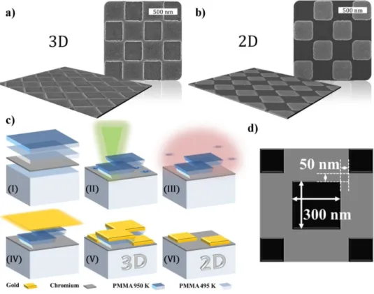
Fig. 1. Perspective and plan-view SEM images of the fabricated 3D (a) and 2D (b) plasmonic structures. (c) Process flow illustrated step by step: (I) On pre-deposited 5 nm chromium, PMMA 495 K and PMMA 950 K are spin-coated, respectively. (II) Electron beam scans the pattern on PMMA resist. (III) O2 plasma cleaning removes the PMMA residues remained after developing. (IV) 40 nm thick gold is thermally deposited. (V) The 3D-structure fabrication is completed and (VI) an additional lift-off step is required for the 2D-structure. (d) EBL mask layout shown with important features.
2. Fabrication and structural characterization
As a model structure of the nanoplasmonic three-dimensional surface, we studied a modified checkerboard array with intentional gaps between the two adjacent squares composed of two complementary 2D layouts separated by an interplanar distance (Fig. 1(a)). Our modified checkerboard design, which allows for a simpler fabrication process, is different than the standard checkerboard pattern employing structures in 2D [15,16] and in 3D [29] form, which is shown to be a good SERS platform. The modified checkerboard with intentional gaps achieves highly reproducible results of high electric field enhancement with easy fabrication. The inherent polarization insensitivity of the checkerboard structure stems from the two-fold rotational symmetry, which simplified the analysis of the numerical and experimental results, and relatively large feature sizes provide high reproducibility. For the implementation of the proposed architecture, we developed the fabrication process flow of the 3D- and structures, following the similar steps except for the final lift-off step required in the 2D-structure (Fig. 1(b)). We used 350 μm thick double side polished fused quartz wafers as the substrate having well known optical properties, making optical measurements and numerical simulations compatible and reliable. As illustrated in Fig. 1(c), using electron beam deposition, a 5 nm thick chromium layer was coated on the substrate serving as the adhesion promoter for bottom gold layer, preventing charging effects during electron-beam lithography (EBL) process and making possible of imaging the structures after fabrication with scanning electron microscopy (SEM). As discussed in the literature, sidewall formation here can reduce the field enhancement [29]. To prevent the sidewall formation in the 3D-structure and facilitate the lift-off process for the 2D-structure, a bilayer poly(methyl methacrylate) (PMMA) film consisting of PMMA 495 K and PMMA 950 K molecular weight layers were spin-coated as the EBL resist, which provides undercut following the development step (as sketched in (I) of Fig. 1(c)). After 5 min prebake on hotplate at 180 °C, PMMA 495 K with A2 concentration is spin-coated at 5000 rpm rate for 45 s. Immediately, 90 s postbake is applied and the second layer is coated with PMMA 950 K in A2 concentration, which has a higher molecular mass compared to the PMMA 495, again at 5000 rpm for 45 s. Finally, 10 min postbake is applied to provide a smooth PMMA surface. Subsequently the EBL step using the layout given in Fig. 1(d) is performed (as illustrated in (II) of Fig. 1(c)). EBL is performed using Nova NanoSEM 600 from FEI integrated with ElphyPlus from Raith as a lithography controller. To define the sharp corners of the checkerboard, we used the electron beam current at 32 pA with a 30 kV accelerating voltage, which reduces the radius of the electron beam onto the resist. As an optimum area dosage we used 300 μC/cm2. After electron
beam scanning, PMMA developed in a mixture of methyl isobutyl ketone (MIBK) and isopropanol alcohol (IPA) with a 1:3 ratio from MicroChem Corp. for 13 s and then rinsed in extra pure IPA solution for 20 s. To remove the residues of PMMA during the development step, O2 plasma cleaning for 30 s is required (as shown in (III) of Fig. 1(c)). O2 plasma
cleaning was also used to control the thickness of the patterned PMMA bilayer, which was initially about 120 nm. From our early coarse simulations (not presented here), we observed that the PMMA layer should be thinner than 100 nm to increase the coupling between the upper-lower planes. On the other hand, to safely prevent sidewall formation between them, the PMMA layer should be about two times thicker than the gold film, which makes 80 nm for the total film thickness of the bilayer PMMA film. Similarly, early simulations indicate that gold films should be as thin as possible, however, in the case of up to 30 nm mass thickness, nanoislands can form, preventing continuous film formation. To be on the safe side, we decided on using a 40 nm thick gold film on top of the patterned bilayer PMMA, which was deposited using thermal deposition under vacuum environment (as sketched in (IV) of Fig. 1(c)). During deposition, to facilitate adhesion of gold on PMMA (for the structure top layer) and on chromium (both for the 2D-structure and bottom layer of 3D-structure) first a 15 nm thick gold is coated relatively fast at a rate of 0.07 nm/s and, for the
remaining 25 nm, a smooth surface is attained by coating gold at a rate of 0.04 nm/s. Although the fabrication of the 3D-structure is finalized at this point (see (V) of Fig. 1(c)), an additional lift-off step for the 2D-structure is required (as given in (VI) of Fig. 1(c)). Lift-off is performed by keeping the substrate in 1,2-dichloroethane, having shown to be a very successful solvent for PMMA [30], for 4 hours followed by instant dipping in ultrasonic bath.
Fig. 2. (a) Cross-sectional SEM image of the 3D-structure showing no sidewall formation between two planes. Atomic force microscopy topographic images of the 2D- (b) and 3D- (c) structures indicating a gold thickness of 40 nm and a pit depth of 80 nm.
After several iterations of simulations and experimental measurements, we worked with checkerboard structures having squares of 300 nm side length separated by 50 nm in lateral directions (Fig. 1(d)). SEM images of these resulting plasmonic structures are shown in Fig. 1(a) for the 3D-architecture and in Fig. 1(b) for the 2D-architecture. Perspective SEM images are obtained with a 35°-tilted stage, along with an artificial post-imaging rotation for demonstrative purposes. In these images of the 2D-structure bright parts correspond to gold structures and dark background is due to Cr layer coated on the fused silica wafer. Since the 3D-structure is coated with gold everywhere, the plan-view image consists of bright areas. The fabricated structure feature sizes are in good agreement with the simulated structures and rounded corners observed both in the 2D- and 3D-structures, which are taken into account by using of rounded corners having a 40 nm radius in the simulation setup. The undercut formation in the 3D-structure was observed using the cross-sectional SEM image obtained by focused ion beam etch technique. First, a protective platinum layer is deposited using electron beam at very slow rates to prevent milling during deposition. Then, the second platinum deposition at a high deposition rate using ion beam is performed. The difference between two layers can be observed in Fig. 2(a). Finally, ion milling is performed and a cross-sectional image is obtained on a similar device. Although no sign of sidewall formation is evident from the performing lift-off step for 2D-structure, the profile of the cross-section gives additional data to explain the differences between the simulated structure and the fabricated one. The bending of the upper layer around the corner is the main observed difference between them. To measure the gold thickness in the 2D-structure and the pit depth in the 3D-structure we used AFM measurements that gives a gold thickness of 40 nm and a pit depth of 80 nm between the two complementary layers of the 3D-structure as shown in Fig. 2(b) and 2(c), respectively.
Fig. 3. (a) Electron-beam lithography fabrication layout indicating important size parameters along with the unit cell used in EBL for laying out the design structure marked with a red square. (b) Equivalent diagonal simulation configuration shown with the unit cell in the red square used in numerical simulations. This layout is identical to the one given in (a).
3. Numerical simulations and results
Numerical simulations are performed using commercially available finite-difference time-domain solver, called FDTD Solutions, from Lumerical Inc. using 3D simulation environment under impinging plane wave at a single wavelength varied with 5 nm steps incident from the air side. As material refractive index data we used ellipsometry measurements for gold and chromium. For fused quartz we used material library of the software and the bilayer PMMA refractive index is taken 1.485 with no imaginary part (no loss). The conventional unit cell used in EBL patterning is presented in Fig. 3(a) and to reduce the computational requirements, simulation area is defined periodically with a diagonal unit cell configuration as given in Fig. 3(b). Figure 4(a)-4(d) show the cross-sectional nearfield intensity distribution maps of the simulated 3D- and 2D-structures as well as those of the upper plane and the lower plane components alone, which together make up the full 3D-structure, at 580 nm illumination wavelength as the localized surface plasmon (LSP) resonance of the 3D-structure. As shown in Fig. 4, we excite the structure with a plane wave source in the -z direction with the polarization along the x direction having unity intensity in all wavelengths corresponding to 0 level in the logarithmic scale. Simulated unit cell is indicated with the red square in the middle placed under the x-z and y-z plane maps for all structures. For each structure field map, x-z and y-z planes are parallel and perpendicular to the source polarization, respectively. Four equally spaced x-y plane maps correspond to critical z levels of the structure as shown in the cross-sectional side view in the middle: z = 5 nm is the starting point of the structure, just above the chromium layer; z = 45 nm is the top of the lower gold plane (corresponding to 2D-structure without PMMA pillars around it); z = 85 nm is the top of the PMMA layers and the bottom of the upper gold layer (which is the complementary form of the 2D-structure); and finally z = 125 nm corresponds to top of the upper plane of the structure (also top of the overall structure).
Fig. 4. Simulation results showing electric field intensity distributions for the 3D- (a), the 2D- (b), the upper plane (c) and the lower plane (d) structures. Important positions along z-direction and the components of the upper and lower plane structures are illustrated (e). Percent extinction of the simulated structures showing coupling between the upper and lower planes in the 3D-structure (f). Nearfield intensity distributions of the 3D-structure at the same specific cross-sectional planes as in (a) are plotted for illumination with varying wavelength as a movie (Media 1).
Field intensity is normalized with respect to the incoming source intensity and mapped in the logarithmic color scale. Here the upper plane contains the partial structure remaining after removal of the gold plane between z = 5 and z = 45 nm; and, in a complementary fashion, the lower plane consists of the partial structure remaining after the gold layer between z = 85 nm and z = 125 nm is removed (Fig. 4(e)). To relate the numerical results with the experimental measurements, in Fig. 4(f) we present the farfield extinction of the 3D-, 2D-, upper plane and lower plane structures. Here the blue-shifted and stronger LSP resonance of the 3D-structure with respect to that of the upper plane structure suggests that the resonance of the 3D-structure results from the coupling between the upper and lower plane 3D-structures. Figure 4(a) shows that the 3D-structure is superior to the other structures, with its volumetric field enhancement reaching a maximum field enhancement factor 7.2 times larger than that of the 2D-structure. Note that the enhancement of 2D-structure occurs only around the sides of the square, limiting the field enhancement into a small region as expected. Another interesting observation is that the lower plane structure shows higher extinction than 2D-structure, although they have similar structures except for the PMMA pillars left between the gold squares in the lower plane structure.
Fig. 5. (a) 3D-structure-like grating structure with specified dimensions shown for TM excitation configuration. (b) Resulting extinction for a given grating structure with TM, TE and unpolarized illuminations compared with the 3D- and 2D-structures. Nearfield intensity distributions in logarithmic scale for the resonance wavelengths 580 nm (c) and 715 nm (d).
To understand the coupling mechanism in the 3D-structure and effect of the periodicity in the checkerboard structure we modeled a 3D-like grating with similar periodicity and size properties to our 3D-surface as shown in Fig. 5(a). From the simulated extinction in Fig. 5(b) for the 3D, 2D and 3D-like grating structure (under electric (TE), transverse-magnetic (TM) and unpolarized illumination) we observe that only TM illumination is coupled to the grating structure indicating surface plasmon polariton coupling at 715 nm wavelength [31]. The peak around 715 nm is also present in the 2D-structure and this effect can be explained by the grating counterpart of the 3D checkerboard structure. It is evident that two resonances observed at 580 nm (Fig. 5(c)) and 715 nm (Fig. 5(d)) in the 3D-like grating structure are the two modes of the 3D-structure and the 2D-structure, respectively. Both of these two resonances exhibit the coupling behavior between the upper and lower plane, while the resonance at 715 nm occurs stronger than the resonance at 580 nm. The weak resonance at 580 nm observed in the 3D-like grating is significantly enhanced in the 3D-structure, which can be attributed to LSP resonance behavior.
As discussed earlier, the main motivation for choosing the checkerboard structure is its two-fold symmetry resulting in polarization insensitivity. As observed from Fig. 5(b), the 3D-like grating structure shows quite strong resonance in the TM illumination case; however, it exhibits almost no resonance under the TE illumination since surface plasmon polaritons cannot be excited with the TE excitation. If we take their average response as the unpolarized light response, which is also presented in Fig. 5(b), the strength of the 3D checkerboard structure is more evident since its response will be the same for all illumination types under normal incidence.
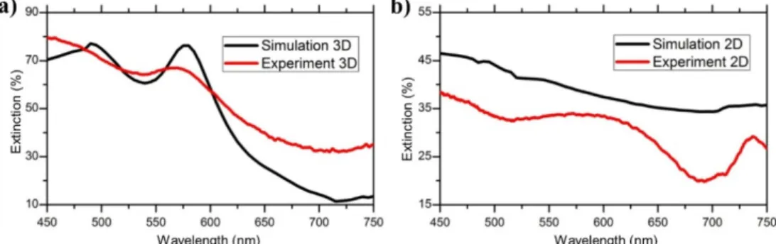
Fig. 6. Comparison of simulated and experimental farfield extinction of the 3D- (a) and 2D- (b) structures.
4. Experimental results
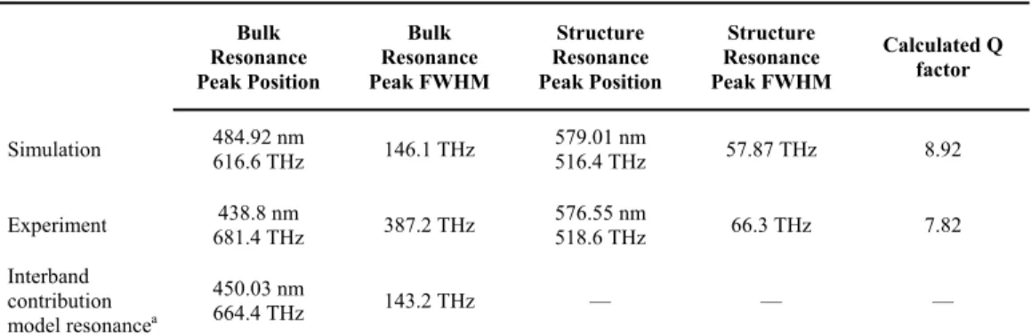
Numerical simulations are verified by comparison with the experimental extinction measurements. Figure 6(a) and 6(b) show the comparison of numerical simulation and experimental measurement results for the and 2D-structures, respectively. For the 3D-structure we analyzed the LSP peak at 580 nm by modeling the observed resonance as a Lorentzian peak (Fig. 7). The resulting quality factor is found to be 8.92 for the simulation results (Fig. 7(a)) and 7.82 for the experimental results (Fig. 7(b)), Also, the resonance is centered at 579.0 nm for the numerical simulation and 576.6 nm for the experimental measurement (see Table 1) indicating strong correlation between these results. The reduction in the quality factor of the resonance in the case of experimental characterization can be due to the bending of the corners observed from the cross-sectional image of the 3D-checkerboard structure in Fig. 2(a).
Fig. 7. (a) Lorentzian peak fit to simulated extinction with two peaks. (b) Lorentzian peak fit to experimental extinction with two peaks.
Table 1. Two Lorentzian peaks fit results for simulation and experiment. Bulk Resonance Peak Position Bulk Resonance Peak FWHM Structure Resonance Peak Position Structure Resonance Peak FWHM Calculated Q factor Simulation 484.92 nm 616.6 THz 146.1 THz 579.01 nm 516.4 THz 57.87 THz 8.92 Experiment 681.4 THz 438.8 nm 387.2 THz 576.55 nm 518.6 THz 66.3 THz 7.82 Interband contribution model resonancea 450.03 nm 664.4 THz 143.2 THz — — —
a L. Novotny and B. Hecht, Principles of Nano-Optics (Cambridge University Press, 2006). 5. Conclusion
In conclusion, the proposed 3D-nanoplasmonic surfaces provide volumetric electric field intensity enhancement, significantly stronger than the 2D planar counterparts, as verified by the numerical simulations agreeing well with the experimental farfield measurements. With the surface-normal field enhancement observed in the 3D-structure, the maximum enhancement factor is found to be 7.2 times larger than that in the 2D-structure. This showcases the strength and potential of such 3D-nanoplasmonic surfaces, in addition to the reduced complexity of the 3D-structure fabrication compared to widely-used conventional 2D-plasmonic structures.
Acknowledgments
This work is supported by EC-FP7 N4E NoE and TUBITAK EEEAG 110E010, 110E217, 111E189 and 112E183, and in part by NRF-RF-2009-09 and NRF-CRP-6-2010-02. H.V.D. acknowledges support from ESF-EURYI and TUBA-GEBIP; and K.G. from TUBITAK BIDEB 2211 and 2214.