INSTITUTE OF PHYSICS PUBLISHING SEMICONDUCTOR SCIENCE AND TECHNOLOGY
Semicond. Sci. Technol. 17 (2002) L59–L62 PII: S0268-1242(02)39380-5
LETTERTOTHEEDITOR
Electron initiated impact ionization in
AlGaN alloys
C Bulutay
Department of Physics, Bilkent University, Ankara, 06533, Turkey
Received 11 July 2002, in final form 22 August 2002 Published 19 September 2002
Online at stacks.iop.org/SST/17/L59 Abstract
Detailed impact ionization (II) analysis of electrons is presented for AlGaN alloys as a vital resource for solar-blind avalanche photodiode and high power transistor applications. Necessary ingredients for the II
characterization are supplied from a recent experiment on the GaN end, and a Keldysh analysis for the AlN end, of the alloy AlGaN. High-field electron dynamics are simulated using an ensemble Monte Carlo framework, accounting for all valleys in the lowest two conduction bands, obtained from accurate empirical pseudopotential band structure computations. The effect of alloy scattering on II is considered and observed to be significant. For any
AlxGa1−xN alloy, the electron II coefficients are found to obey the form,
A exp(−K/F), for the electric field, F.
The AlxGa1−xN alloy is emerging as a complementary material
system for high power electronic and optoelectronic applications. Specifically, GaN/AlxGa1−xN heterojunction
bipolar transistors and AlxGa1−xN avalanche photodiodes
(especially for solar-blind purposes) are two important devices to benefit from this material system. For both these devices, operating at high fields, it is compulsory to understand the impact ionization (II) process. However, there has been no experimental work on II for the AlxGa1−xN
system. As a matter of fact, measurement of the II coefficient is rather a formidable task, which requires maintaining uniform fields and avoiding instabilities [1]. To meet this demand from the computational side, in this letter we provide results for the characterization of electron initiated II in AlxGa1−xN for a
wide range of alloy compositions.
We utilize our accurate band structures for GaN and AlN [2, 3] based on the empirical pseudopotential technique fitted to available experimental results and first-principles computations, with special emphasis given to conduction band properties. For the band structure of the alloy,
AlxGa1−xN, we resort to linear interpolation (Vegard’s law)
between the pseudopotential form factors of the constituent binaries as, for instance, in the work of Goano et al [4] Our approach for high-field transport relies on the ensemble Monte Carlo (EMC) technique [5], including all major scattering processes: acoustic, non-polar and polar optical phonons, ionized impurity, alloy and II scatterings. We consider the initial free carrier density to be low, so that the carrier–carrier scattering can be neglected; of course, after the initiation of an II breakdown, there may be a large carrier density where this scattering mechanism becomes significant.
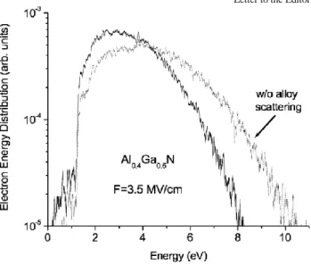
PriortoEMCsimulation, weperformabandedgeanalysis throughout the computed bands of AlxGa1−xN, and extract the
band edge energy, effective mass and non-parabolicity parameters of all valleys in the lowest two conduction bands, which are located at 1, U, K, M and 3 points. To account for the remaining excited bands, we further append an additional higher-lying parabolic free electron band. Table 1 lists these parameters for the alloy mole fractions used in this work. In lieu of this band pre-processing, we can now proceed to use the computationally appealing analytical-band variant of the
EMC technique. It may be noted that more sophisticated full band EMC approaches exist, as applied to GaN [6, 7]. Despite the poor representation of the band structure at higher energies for a model like ours, it has been tested to reproduce the experimental as well as full band results in the same context of II in bulk and p–i–n diodes [8, 9]. Furthermore, the computational overhead of a full band EMC simulation should
also be kept in mind. As a matter of fact, II is a rare event among allelectrons, and requires accurate representation of carriers in the high-energy tail of the distribution function. Thus, we employ 25 000 electrons in the ensemble, with a time stepoflessthan0.1fs, andatotalsimulation timeofabout 1ps.
0268-1242/02/100059+04$30.00 © 2002 IOP Publishing Ltd Printed in the UK L59
Letter to the Editor
Table 1. Band edge analysis throughout the lowest two conduction bands of AlxGa1−xN alloys; E is the band edge energy, m∗ is the density
of states effective mass and α is the non-parabolicityfactor (other than the lowest valley, two-band values are preferred). Equivalent valley multiplicities Nv are also included. Note that the ordering of the U and K valleys is interchangedat an aluminium mole fraction of 0.6.
E (eV) ∗/ α (eV−1) GaN Al0.2 0.8 0.4 0.6 0.6 0.4 0.8 0.2 U (Nv = 6) 1.34 0.442 1.285 0.456 1.233 0.468 1.181 0.486 1.131 0.487 1.05 0.495 0.064 0.056 0.049 0.043 0.039 0.035 K (Nv = 2) 1.59 0.47 1.444 0.477 1.307 0.483 1.179 0.478 1.057 0.488 0.9 0.488 0.055 0.050 0.045 0.042 0.039 0.106 M (Nv = 3) 1.87 0.565 1.830 0.577 1.798 0.590 1.769 0.604 1.741 0.617 1.68 0.629 0.035 0.030 0.026 0.023 0.020 0.017 1) 2.14 2.23 2.312 2.390 2.462 2.49 0.439 0.463 0.485 0.507 0.529 0.55 0.056 0.046 0.039 0.032 0.027 0.023 Free electron 3.5 3.6 3.7 3.8 3.9 4 band (Nv = 1) 1 0 1 0 1 0 1 0 1 0 1 0
Table 2. A and K values in the electron II coefficient expression, A exp(−K/F), where F is the electric field. A temperature of 300 K and an ionized impurity concentration of 1017
cm−3 are used. GaN Al0.2Ga0.8N Al0.4Ga0.6N Al0.6Ga0.4N Al0.8Ga0.2N AlN A (cm−1) K (MV cm−1) 1.1438 × 10⁷ 23.8933 1.5126 × 10⁷ 31.6707 2.0647 × 10⁷ 36.6251 1.7974 × 10⁷ 37.7751 1.2993 × 10⁷ 36.3373 8.8750 × 10⁶ 37.5904
With this parameter set, we can resolve fast processes while assuring steady-state operation for all fields considered.
The only available experimental report about II relevant to our work is that on GaN by Kunihiro et al [10]. Using our
EMC framework, we are able to fit to their electron ionization coefficient with an II scattering rate of PIIGaN(1/s) =
2.5 × 10⁶ Ein, where Ein is the
electronvolts, EthGaN = 4 eV is the II threshold energy, and u(·) is the unit step function. This expression, when compared to the ab initio results for GaN [11], possesses similar exponent and threshold values, but a reduced coefficient. On the other hand, for AlxGa1−xN Ando et al [7] have used linear
interpolation between the II rates of GaN and AlN, assuming for simplicity a null value for AlN. Aiming for a more realistic estimation for AlN, we make use of the Keldysh approach, which is valid for parabolic bands, while Bloch overlaps are taken into account via the f-sum rule [12]. The corresponding II scattering rate comes out as PIIAlN in EAlN 2u E EthAlN, where EthAlN = 6.84 eV. Examining the forms of these two scattering rate expressions, we see that GaN possesses a soft threshold, whereas the Keldysh treatment
demands a hard
thresholdforAlN.Thelattershouldnotbeunderminedaswell; as Hess pointed out, the Keldysh approach can still adequately represent the experimental data for the case of steady-state phenomena [1]. L60
During the EMC simulation we keep a fixed carrier population, and after an II event we discard the generated electron–hole pair. However, for the purposes of this work we are more sensitive to the energy loss of the impacting electron and we avoid the simplistic treatment of restarting this electron from the conduction band minimum, as is usually done
[7, 13]. Utilizing the results of first-principles characterization on II by Jung et al [14], we employ a piecewise linear functional relation between the initial (Ein) and final (Efin) energies of the impacting electron, measured from the conduction band minimum, as
0, Ein < EAB
Efin =in EbrAB
in,
where ,
and EthAB is the alloy II threshold energy obtained using Vegard’s law from the binaries EthA and EthB. The energy coefficients above, c1, c2 and c3, are practically taken to be material independent [15], and we use the values of Jung et al, c1 = 0.55, c2 = 0.267, c3 = 2.11, extracted from GaAs data at 300 K [14]. Incorporating the first-principles II scattering rate expression of this reference to our EMC formalism yields excellent agreement with the experimental results for GaAs [10], making us confident about the validity of this approach.
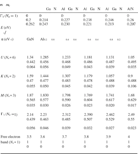
Figure 1. Electron II coefficient versus inverse electric field. Dotted curves indicate the results when alloy scattering is not included. The curves for Al0.6Ga0.4N and Al0.8Ga0.2N merge at higher fields. These
results are obtained for a temperature of 300 K and an ionized impurity concentration of 1017 cm−3.
Returning to the AlxGa1−xN system, the electron II
coefficient, α, for several alloy compositions are plotted in figure 1 with respect to the electric field, F. These results are obtained for a temperature of 300 K and an ionized impurity concentration of 1017 cm−3. We note that these curves do not obey Wolff’s form, A exp(−K/F2), but rather can be faithfully represented using Shockley’s form of A exp(−K/F); refer to table 2 for a list of these constants, A and K. In this regard, we find it useful to add the remark of Bude and Hess [16] that the functional dependence of α on F is closely related to the rise of the density of states in the most important energy range, and not as much to the question of whether lucky electrons are important for ionization or not.
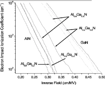
Inasemiconductor alloy, the scatteringoffreecarriers due to deviations from the virtual crystal model, as also employed in this work, has been termed alloy scattering [12]. Recently, Farahmand and Brennan [17] have addressed alloy scattering in group-III nitride ternary alloys, using the conduction band offset between the binaries as the alloy potential. They have argued that this approach yields an upper bound for alloy scattering. As a representative value, in our work we use Ualloy = 0.91 eV, which is half the corresponding GaN/AlN conduction band offset. The dotted curves in figure 1, corresponding to aluminium mole fractions of 0.2 and 0.4, indicate that when alloy scattering is turned off II is significantly enhanced. In contrast, the elastic nature of the alloy scattering might initially suggest a marginal effect on the electron energy distribution. However, the deviation of the electron wave vector away from the electric field due to elastic scattering causes deceleration in the drift cycles, hence a loss in the energy of such an electron, lowering its potential for II. Figure 2 illustrates this point for Al0.4Ga0.6N (which is an important alloy composition for solar-blind applications) at an electric field value of 3.5 MV cm−1; the depletion of the high-energy tail of the distribution function due to alloy scattering
explains the decrease in the II coefficient obtained in figure 1. However, we would like to draw attention to two simplifications in our approach inherited from the treatment of
Letter to the Editor
Figure 2. Electron energy distribution for Al0.4Ga0.6N at an electric
field of 3.5 MV cm−1, with (solid curve) and without (dotted curve)
alloy scattering. A temperature of 300 K and an ionized impurity concentration of 1017
cm−3 are considered.
FischettiandLaux[18]. Thealloyscatteringisimplementedas an intra-valley process due to its small wavelength attenuation [18]; in the case of closely located valleys, such as U and M, this may become rather crude. More importantly, the distribution of the final scattering angles is assumed to be isotropic, even though at higher energies alloy scattering attains a forward directional character [19]. Thus, we are led to think that the effect of the alloy scattering may still be somewhat overestimated.
In summary, we present results for the electron II coefficient of AlGaN alloys and we offer closed form expressions for its functional dependence for a wide range of alloy compositions. A detailed discussion of the role of alloy scattering in this context is also included. We hope that this work will initiate further experimental and theoretical studies. Acknowledgments
The author would like to express his gratitude to Professor K Tomizawa. This work is supported by the Scientific and Technical Research Council of Turkey (TUB¨ ˙ITAK).
References
[1] Balkan N, Ridley B K and Vickers A J (ed) 1993 Negative Differential Resistance and Instabilities in 2-D Semiconductors(New York: Plenum)
[2] Bulutay C, Ridley B K and Zakhleniuk N A 2000 Phys. Rev. B
62 15754
[3] Bulutay C, Ridley B K and Zakhleniuk N A 2002 Physica B 314 63
[4] Goano M, Bellotti M E, Ghillino E, Garetto C, Ghione G and Brennan K F 2000 J. Appl. Phys. 88 6476
[5] Tomizawa K 1993 Numerical Simulation of Submicron SemiconductorDevices (Norwood: Artech)
[6] Koln´ık J, Oguzman˘ ˙I H, Brennan K F, Wang R and Ruden P P
1997 J. Appl. Phys. 81 726
[7] Ando Y et al 2000 IEEE Trans. Electron Devices 47 1965 [8] Dunn G M, Rees G J, David J P R, Plimmer S A and
Herbert D C 1997 Semicond. Sci. Technol. 12 111
L61 Letter to the Editor
[9] Dunn G M, Ghin R, Rees G J, David J P R, Plimmer S and Herbert D C 1999 Semicond. Sci. Technol. 14 994
[10] Kunihiro K, Kasahara K, Takahashi Y and Ohno Y 1999 IEEE Electron Device Lett. 20 608
[11] Reigrotzki M, Dur M, Schattke W, Fitzer N, Redmer R and¨ Goodnick S M 1997 Phys. Status Solidi b 204 528
[12] Ferry D K 2000 Semiconductor Transport (London: Taylor and Francis)
[13] Farahmand M and Brennan K F 1999 IEEE Trans. Electron Devices 46 1319
L62
[14] Jung H K, Nakano H and Taniguchi T 1999 Physica B 272 244 [15] Mouton O, Thobel J L and Fauquembergue R 1997 J. Appl. Phys. 81 3160
[16] Bude J and Hess K 1992 J. Appl. Phys. 72 3554
[17] Farahmand M, Garetto C, Bellotti E, Brennan K F, Goano M, Ghillino E, Ghione G, Albrecht J D and Ruden P P 2001 IEEE Trans. Electron Devices 48 535
[18] Fischetti M V and Laux S E 1996 J. Appl. Phys. 80 2234 [19] Yeom K, Hinckley J M and Singh J 1996 J. Appl. Phys. 80