DESIGN OF APPLICATION SPECIFIC INSTRUCTION
SET PROCESSORS FOR THE FFT AND FHT
ALGORITHMS
a thesis
submitted to the department of electrical and
electronics engineering
and the institute of engineering and sciences
of bilkent university
in partial fulfillment of the requirements
for the degree of
master of science
By
O˘guzhan Atak
September 2006
I certify that I have read this thesis and that in my opinion it is fully adequate, in scope and in quality, as a thesis for the degree of Master of Science.
Prof. Dr. Abdullah Atalar(Supervisor)
I certify that I have read this thesis and that in my opinion it is fully adequate, in scope and in quality, as a thesis for the degree of Master of Science.
Prof. Dr. Murat A¸skar
I certify that I have read this thesis and that in my opinion it is fully adequate, in scope and in quality, as a thesis for the degree of Master of Science.
Prof. Dr. Hayrettin K¨oymen
Approved for the Institute of Engineering and Sciences:
Prof. Dr. Mehmet Baray
ABSTRACT
DESIGN OF APPLICATION SPECIFIC INSTRUCTION
SET PROCESSORS FOR THE FFT AND FHT
ALGORITHMS
O˘guzhan Atak
M.S. in Electrical and Electronics Engineering
Supervisor:
Prof. Dr. Abdullah Atalar
September 2006
Orthogonal Frequency Division Multiplexing (OFDM) is a multicarrier trans-mission technique which is used in many digital communication systems. In this technique, Fast Fourier Transformation (FFT) and inverse FFT (IFFT) are kernel processing blocks which are used for data modulation and demodulation respectively. Another algorithm which can be used for multi-carrier transmission is the Fast Hartley Transform algorithm. The FHT is a real valued transforma-tion and can give significantly better results than FFT algorithm in terms of energy efficiency, speed and die area. This thesis presents Application Specific Instruction Set Processors (ASIP) for the FFT and FHT algorithms. ASIPs combine the flexibility of general purpose processors and efficiency of application specific integrated circuits (ASIC). Programmability makes the processor flexible and special instructions, memory architecture and pipeline makes the processor efficient.
In order to design a low power processor we have selected the recently pro-posed cached FFT algorithm which outperforms standard FFT. For the cached FFT algorithm we have designed two ASIPs one having a single execution unit
and the other having four execution units. For the FHT algorithm we have derived the cached FHT algorithm and designed two ASIPs; one for the FHT and one for the cached FHT algorithm. We have modeled these processors with an Architecture Description Language (ADL) called Language of Instruction Set Architectures (LISA). The LISATek processor designer, generates the software tool chain (assembler, linker and instruction set simulator) and HDL code of the processor from the model in LISA automatically. The generated HDL code is further synthesized into gate-level description by Synopsis Design Compiler with 0.13 micron technology library and then power simulations are performed. The single execution unit cached FFT processor have been shown to save 25% of en-ergy consumption as compared to an FFT ASIP. The four execution unit cached FFT processor on the other hand runs faster up to 186%. The ASIP designed for the developed cached FHT algorithm runs almost two times faster than the ASIP for the FHT algorithm.
Keywords: FFT, cached FFT, FHT, cached FHT, Applicattion Specific
¨
OZET
FFT VE FHT ALGORITMALARI ˙IC˙IN UYGULAMAYA ¨
OZG ¨
U
KOMUT K ¨
UMEL˙I ˙ISLEMC˙I TASARIMI
O˘guzhan Atak
Elektrik ve Elektronik M¨uhendisli¯gi B¨ol¨um¨u Y¨uksek Lisans
Tez Y¨oneticisi:
Prof. Dr. Abdullah Atalar
Eyl¨ul 2006
Ortogonal Frekans B¨olmeli C¸ o˘gullama bir¸cok sayısal haberle¸sme sisteminde kullanılan ¸cok ta¸sıyıcılı bir haberle¸sme tekni˘gidir. Bu teknikte hızlı Fourier donusumu (FFT) ve tersine hızlı Fourier donusumu (IFFT) modulleri, sayısal veri modulasyonu ve demodulasyonu icin kullanılan temel mod¨ullerdir. C¸ ok ta¸sıyıcılı sayısal haberle¸sme i¸cin kullanılabilecek bir di˘ger algoritma ise hızlı Hart-ley d¨on¨u¸s¨um¨ud¨ur (FHT). FHT algoritması reel bir d¨on¨u¸s¨um oldu˘gu i¸cin, enerji t¨uketimi, silikon b¨uy¨ukl¨u˘g¨u ve ¸calı¸sma hızı bakımından FFT algoritmasına g¨ore daha iyi sonu¸clar verebilir. Bu tezde, FFT ve FHT algoritmaları i¸cin Uygulamaya
¨
Ozg¨u Komut K¨umeli ˙I¸slemciler sunuyoruz. Uygulamaya ¨ozg¨u i¸slemci y¨ontemi, genel ama¸clı i¸slemcilerin sa˘gladı˘gı esneklik ile, uygulamaya ¨ozg¨u t¨umle¸sik de-vrelerin (ASIC) sa˘gladı˘gı verimlili˘gi birle¸stirmektedir. ˙I¸slemcinin programlan-abilir olması onu esnek ve uygulamaya ¨ozg¨u komutları, bellek mimarisi ve i¸slem hattına (pipeline) sahip olması ise onu verimli yapmaktadır.
D¨u¸s¨uk enerji t¨uketen bir i¸slemci tasarlamak amacıyla, FFT algoritmasına g¨ore daha iyi sonu¸c veren ¨onbellekli-FFT algoritmasını kullandık. Bu algoritma i¸cin, biri tek i¸slev uniteli, di˘geri d¨ort i¸slev uniteli olmak ¨uzere iki i¸slemci tasar-ladık. FHT algoritması i¸cin ise ¨onbellekli-FHT algoritmasını geli¸stirdik ve biri
FHT algoritması i¸cin ve di˘geri ¨onbellekli FHT algoritması i¸cin iki i¸slemci tasar-ladık. Bu i¸slemcilerin tasarımını komut k¨umesi mimari dili (LISA) adı verilen bir mimari tanımlama dili ile yaptık. Bu dil i¸cin geli¸stirilmi¸s bir yazılım aracı; LISATek i¸slemci tasarımcısı, tasarlanan i¸slemcinin yazılım geli¸stirme araclarını (assembler, linker, komut k¨umesi simulatoru) ve HDL (Hardware Description Language) kodunu otomatik olarak ¨uretmektedir. Uretilen HDL kodunu ise¨ UMC 0.13 micron teknoloji k¨ut¨uphanesini kullanarak, Synopsis Design Compiler yazılım aracı ile sentezleyerek mantık devresi seviyesinde HDL kodu elde ettik ve enerji t¨uketimi simulasyonları yaptık. Tasarladı˘gımız tek i¸slev ¨uniteli ¨onbellekli-FFT i¸slemcisi aynı metodla tasarlanmı¸s bir ¨onbellekli-FFT i¸semcisine g¨ore %25 enerji tasar-rafu sa˘glamaktadır. D¨ort i¸slev ¨uniteli ¨onbellekli-FFT i¸slemcisi ise %186 ya kadar daha hızlı ¸calı¸sabilmektedir. FHT algoritması i¸cin tasarladı˘gımız, ¨onbellekli-FHT i¸slemcisi ise FHT i¸slemcisine g¨ore yakla¸sık iki kat daha hızlı ¸calı¸smaktadır.
-Anahtar Kelimeler: Hızlı Fourier D¨on¨u¸s¨um¨u, FFT, Hızlı Hartley D¨on¨u¸s¨um¨u, FHT, ¨onbellekli FFT, ¨onbellekli FHT, Uygulamaya ¨Ozg¨u Komut K¨umeli ˙I¸slemci, Ortogonal Frekans B¨olmeli C¸ o˘gullama
ACKNOWLEDGMENTS
I would like to thank Prof. Abdullah Atalar and Prof. Erdal Arıkan for their guidance and supervision during the course of my master study. I would also like to thank Prof. Gerd Ascheid for hosting me at the Institute of Integrated Systems, Technical University of Aachen. Special thanks to Harold Ishebabi, David Kammler and Mario Nicola. I would also like to thank my family for their support and patience during my studies.
Contents
1 Introduction 1
1.2 Organization of the Thesis . . . 3
2 Design Methodology 4 2.1 Digital Application Design . . . 4
2.2 ASIP Design . . . 5
2.3 LISA Based Design Methodology . . . 6
2.4 ASIP modeling in LISA . . . 7
2.4.1 RESOURCE section in LISA . . . 8
2.4.2 OPERATION section in LISA . . . 10
2.4.3 Pipeline management . . . 12
2.5 Design Flow . . . 13
3 Cached FFT ASIP 16 3.1 The FFT Algorithm . . . 16
3.1.1 The Cached FFT Algorithm . . . 18
3.1.2 The Modified cached FFT Algorithm . . . 23
3.2 Architectures for the Cached FFT Algorithm . . . 24
3.2.1 Instruction-Set Design . . . 25
3.2.2 The SISD Architecture . . . 28
3.2.3 The VLIW Architecture . . . 29
4 Cached Fast Hartley Transform ASIP 32 4.1 The Fast Hartley Transform Algorithm . . . 32
4.1.1 Structure Of The FHT Algorithm . . . 35
4.1.2 Memory Addressing . . . 36
4.1.3 Dual-Butterfly Computation . . . 37
4.2 Cached Fast Hartley Transform Algorithm . . . 37
4.2.1 Derivation of Cached FHT Algorithm . . . 38
4.3 Processors For The FHT Algorithm . . . 40
4.3.1 FHT Processor . . . 40
4.3.2 Cached FHT Processor . . . 42
5 Results and Conclusion 44 5.1 Implementation Results for cached FFT ASIP . . . 44
List of Figures
2.1 LISA Based Design Flow . . . 6
2.2 Design Flow . . . 15
3.1 Radix-2 FFT Flow-graph . . . 17
3.2 64-point FFT Algorithm . . . 20
3.3 64-point Cached FFT Algorithm . . . 21
3.4 Modified Cached FFT Algorithm . . . 24
3.5 Structure of the BFLY instruction . . . 27
3.6 The SISD Architecture . . . 28
3.7 The VLIW Architecture showing the BFLY . . . 31
4.1 FHT Flow Graph . . . 35
4.2 FHT Pipeline . . . 41
4.3 FHT Pipeline . . . 43
5.2 Execution Cycles Graphic . . . 46
5.3 Execution Cycles for Different Implementations . . . 47
5.4 Energy Consumption for Different Implementations . . . 47
5.5 Execution Cycles: SISD vs VLIW . . . 48
5.6 Energy Consumption:SISD vs VLIW . . . 48
5.7 Area: SISD vs VLIW . . . 49
5.8 Area: Comparison of FFT and FHT processors . . . 50
5.9 Execution Cycles: Comparison of FFT and FHT processors . . . . 50 5.10 Energy Consumption: Comparison of FFT and FHT processors . 51
List of Tables
3.1 Memory Addressing Scheme for Radix-2 . . . 18
3.2 Memory Addressing Scheme for 64-point FFT . . . 19
3.3 Cache Loading for 64-point FFT . . . 19
3.4 Cache and twiddle addressing . . . 21
3.5 Loading and dumping for N = 256 . . . 22
3.6 Loading and dumping for N = 128 . . . 22
3.7 Twiddle Addressing Scheme for the VLIW ASIP . . . 31
4.1 Memory Addressing For FHT . . . 36
4.2 Cache Loading For The First Epoch . . . 38
4.3 Cache Loading For The Second Epoch . . . 38
Chapter 1
Introduction
Multi Carrier Modulation[1] techniques have been shown to be very effective for channels with severe intersymbol interference. Therefore these techniques have been investigated for standardization. For example, OFDM (Orthogonal Fre-quency Division Multiplexing) is used in many wired and wireless applications. In OFDM Systems, data bits are sent by using multiple sub-carriers in order to obtain both a good performance in highly dispersive channels and a good spec-tral efficiency. Because of its robustness against frequency-selective fading and narrow-band interference, OFDM is applied in many digital wireless communi-cation systems such as Wireless Local Area Networks (WLAN) and Terrestrial Digital Video Broadcasting (DVB-T). MCM technologies use Inverse Discrete Fourier Transform (IDFT) for the modulation and Discrete Fourier Transform (DFT) for the demodulation. The complexities of these transforms are reduced by using their fast versions; Inverse Fast Fourier Transform (IFFT) and Fast Fourier Transform (FFT), respectively. The FFT algorithm, like many other sig-nal processing algorithms has a large number of memory accesses causing high energy consumption in memory. It has been shown that, by employing a small cache, the number of memory accesses can be reduced considerably[2].
FFT is a complex valued transform. When its used to transform a real se-quence, the output of the transform involves redundancy, i.e the spectrum is symmetric around the center. Real-valued transforms for Multicarrier Modula-tion and DemodulaModula-tion has been shown to be possible[3] by using the Discrete Hartley Transform[4]. Moreover,the DHT algorithm can be employed to imple-ment FFT/IFFT for symmetrical sequences [5], for example Asymmetric Digital Subscriber Lines (ADSL) service, which has been selected by the American Na-tional Standards Institute[6] has such a symmetrical structure. That the DHT has also a fast version has already been shown[7].The Fast Hartley Transform (FHT) algorithm has a similar flowgraph to that of FFT.
This thesis presents Application Specific Instruction Set Processor (ASIP) implementations of the FFT and FHT algorithms. ASIPs are programmable processors which have customized instruction-set and memory architecture for a particular application. The advantage of ASIPs as compared to other digi-tal implementation techniques is that ASIPs combine the flexibility of general purpose processors and efficiency of ASICs (Application Specific Integrated Cir-cuit). Keutzer et al[8] shows some evidence for the shift from ASIC to ASIP. The birth of digital signal processors in the early 1980s was mainly due to flexibility requirement of the market. After about some ten years video processors have be-come popular in the market. Currently the driving force to design ASIPs rather than ASICs is not the flexiblity requirement but the difficulties in the design of ASICs. As CMOS technology shrinks to the deep-sub-micron(DSM) geometries, the design of an ASIC becomes more difficult due to multi million dollar CMOS manufacturing costs and expensive design tools. The non-recurring engineering costs can only be affordable for large volume products.
1.2
Organization of the Thesis
The rest of the thesis is organized as follows: the ASIP design methodology is presented in chapter 2. The cached FFT algorithm and the ASIPs designed for the cached FFT algorithm are presented in chapter 3. Chapter 4 presents the FHT algorithm and the two processors designed for the FHT algorithm. The thesis is finalized in chapter 5 by presenting the implementation results for the 4 processors.
Chapter 2
Design Methodology
2.1
Digital Application Design
A digital application can be implemented in three ways; pure software (SW), pure hardware (HW) or mixed SW/HW. In the pure software approach, the designer does not deal with the design of the processor hardware, she selects the proces-sor, possibly a general purpose processor (GPS) or a domain specific processor (DSP), from the market for her particular application and writes the software for the application. The pure software approach is the most flexible and the cheapest solution, and time-to-market is little. The pure hardware approach can be classi-fied as ASIC and reconfigurable hardware i.e. Field Programmable Gate Arrays (FPGA) and Complex Programmable Logic Devices (CPLD). The ASIC method can only be possible for large volume products due to expensive CMOS process-ing costs, and it suffers from flexibility. Even a slight change in the application can not be mapped on to the ASIC after it has been implemented on silicon. Pure software and FPGA implementations mainly suffer from performance and power consumption. As a rule of thumb, software implementation is two orders of magnitude and FPGA implementation is one order of magnitude slower than
the ASIC implementation. Another important parameter in the coming System On Chip era is the Intellectual Property (IP) reuse. Even before physical design it is very difficult to alter a customized ASIC. Mixed HW/SW design combines the benefits of pure software and pure hardware methods. In this technique, the design is portioned into HW and SW parts. The SW part makes the design flexible and the HW part makes the design power efficient and fast. Application Specific Instruction Set Processors (ASIP) fall into this category. ASIPs differ from DSPs or GPSs in that the designer not only writes the software code but also designs the underlying hardware.
2.2
ASIP Design
The design of an ASIP requires following phases[9]:
1. Architecture Exploration 2. Architecture Implementation 3. Application Software Design 4. System Integration
The architecture exploration phase is an iterative process which requires the software development tools assembler, linker, compiler and an Instruction Set Simulator (ISS) in order to profile the algorithm on different architectures. The iteration lasts until finding the best match between the algorithm and the archi-tecture. Each time the processor architecture is changed, the software develop-ment tools and the ISS must also be redesigned accordingly. Separate design of processor architecture and software development tools may cause inconsistencies, therefore ASIPs are generally modeled with more abstract languages called Ar-chitecture Description Languages(ADL). ADLs involve not only the information
about the processor hardware architecture but also about the processor instruc-tion set architecture, memory model and possibly instrucinstruc-tion syntax and coding.
2.3
LISA Based Design Methodology
Language of Instruction Set Architectures (LISA)[9] is an ADL which is devel-oped in Technical University of Aachen (RWTH Aachen). LISA aims to cover all the necessary hardware and software information of the processor so that the design is abstracted in a unified language.
Figure 2.1: LISA Based Design Flow
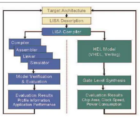
Figure 2.1 shows the LISA based design flow. Once the processor is modeled in LISA, the HDL code, the assembler and linker and the ISS can be generated au-tomatically with the LISA compiler (actually called LISATek Processor Designer, the tool is developed in RWTH Aachen and later acquired by CoWare[10]).
The verification of the processor architecture is done by simulating the desired algorithm on the ISS. This simulation also gives various information about the performance of the processor; such as the number of clock cycles consumed by the algorithm, the distribution of the clock cycles to the instructions, the number of memory hits for each memory and each instruction, the number of clock cycles which is lost during a pipeline stall or flush etc. By using these information, the designer can change the architecture of the processor, she may combine two or more instructions into a single instruction, may decide to include another memory, or invent a new instruction to reduce the effect of the pipeline stalls. On the other side, hardware properties of the processor can be evaluated by performing gate level synthesis and power simulations with third party tools. The LISATek processor designer generates the synthesis scripts for the third party synthesis tools (CADENCE or SYNOPSIS), the designer then synthesize the design into a gate level description(VHDL or VERILOG) and gets the results for the processor area, timing and perform power simulations .
2.4
ASIP modeling in LISA
The processor is modeled in LISA by defining all of the processor resources in a RESOURCE section. The functionality of the processor is modeled by several OPERATIONs which performs operations on the resources defined in the RESOURCE section. Following are the basic language elements of the LISA to model a processor.
2.4.1
RESOURCE section in LISA
All of the processor resources such as RAMs, ROMs, registers and the pipeline, of the processor are defined in this section. A common property for all pro-grammable processors is the program memory, and depending on the needs of the specific algorithm that will eventually run on the processor, several memories can be attached to speed up the processor. All memories of the processor are defined in this section by providing its number of memory locations, the width of the memory locations and the memory flags; X:executable,R:Redable,W:Writable. Below is an example to define a 32 bit program memory and 32 bit data mem-ory of sizes 0x100 and 0x400 respectively. At the beginning of the code is the memory map of the processor.
RESOURCE { MEMORY_MAP{
RANGE(0x0000, 0x00ff) -> prog_mem[(31..0)]; RANGE(0x0100, 0x04ff) -> data_mem[(31..0)]; } RAM unsigned int prog_mem {
SIZE(0x0100); BLOCKSIZE(32,32); FLAGS(R|X);
ENDIANESS(BIG);}; RAM int data_mem{
SIZE(0x0400); BLOCKSIZE(32,32); FLAGS(R|W);
ENDIANESS(BIG); };
/*...other declerations follow*/ }
Another common property of the programmable processors is the registers, all programmable processors require registers for temporary data storage, i.e the input data to the processor may come from the memory, from an I/O device or from the instruction as an immediate value and the algorithm elaborates the input data and stores output values to the processor registers. The registers can be defined as arrays to construct a register file, or can be defined as individual. The third resource that can be defined in the resource section is the processor pipeline. Pipeline refers to the separation of an instruction into multiple clock cycles so that the clock period is reduced, i.e the processor runs faster. Although the instruction is executed in multiple clock cycles, several instructions can be active at different pipeline stages at the same clock cycle, thus the average number of instructions per clock cycle approaches to unity. In LISA, pipeline is defined by declaring the name of the pipeline stages and by declaring the pipeline registers; the registers between pipeline stages. These registers are used by operations assigned to a pipeline stage as the input and output. Below is an example 3 stage pipeline definition with 5 pipeline registers.
RESOURCE{ /*...Other resource declarations*/ PIPELINE pipe = { FE; DE; EX};
PIPELINE_REGISTER IN pipe { unsigned unsigned int instr; short op1; short op2; short op3; short op4; }; }
2.4.2
OPERATION section in LISA
Having modeled the processor resources, the next step is to model the functional-ity of the processor, i.e the usage of the resources. The functionilty is modeled in LISA by OPERATIONs. OPERATIONs assigned to the pipeline stages, model the behavior of the individual pipeline stage. OPERATIONs also model the syntax and coding of the instruction set of the processor. An OPERATION is composed of following subsections:
SY NT AX: is used when the operation is part of a processor instruction and if
it has a syntax.
CODING: defines the binary coding of the instruction, coding section is used
if the operation has to do a decoding.
BEHAV IOR: the operation’s hardware behavior is modeled in this section. Its
input can be either the processor resources defined in RESOURCE section or the operands decoded from SYNTAX and CODING sections. Its output is only the processor resources; the register file, memories or pipeline registers. The syntax used in behavior section for modeling the hardware behavior of the operations is the C language syntax. Thus the designer can define C variables; char, short int, long int for temporary data calculation. The embedded C code for instruc-tion behavior actually corresponds to a hardware descripinstruc-tion. Therefore several data dependent multiplications and/or additions subtractions must be avoided in order not to get a slow processor.
ACT IV AT ION : this section is used to activate other operations in the
follow-ing pipeline stages. Several operations can be activated, the activation order is extracted by the operation’s pipeline stage. Following is an example LISA code section to define a processor with two instructions; ADD and SUB.
OPERATION fetch IN pipe.FE { DECLARE {INSTANCE decode;} BEHAVIOR {
OUT.instr = prog_mem[PC]; OUT.pc = PC;
PC = PC+1; }
ACTIVATION {decode} }
OPERATION decode IN pipe.DE {
DECLARE { GROUP instruction={ADD||SUB}; }
CODING AT (PIPELINE_REGISTER(pipe,FE/DE).pc) { IN.instr == instruction } SYNTAX { instruction }
ACTIVATION { instruction }}
OPERATION ADD IN pipe.EX {
DECLARE {GROUP dst,src={reg};} CODING{0b00 dst src}
SYNTAX{"ADD" ~" " dst "," src} BEHAVIOR{ dst=dst+src }}
OPERATION SUB IN pipe.EX {
DECLARE {GROUP dst,src={reg};} CODING{0b00 dst src}
SYNTAX{"SUB" ~" " dst "," src} BEHAVIOR{ dst=dst-src }}
OPERATION reg {
DECLARE{ LABEL index;} CODING {index=0bx[3]}
SYNTAX {"R[" ~index=#U ~"]"} EXPRESSION{R[index]}
In the above code, the fetch operation is assigned to the FE stage of the pipeline and it simply reads the instruction from the program memory and as-signs the instruction into a pipeline register instr. The ”fetch” operation uncon-ditionally activates the ”decode” operation. The ”decode” operation is assigned to the DE stage of the pipeline. The available instructions are declared as ADD and SUB in the DECLARE section of the ”decode” operation. The decode op-eration simply activates the ADD and SUB opop-erations according to the contents of the pipeline register instr. The ADD and SUB operations are assigned to the EX stage of the pipeline, the operands of both operations are declared as ”dst” and ”src”. These two variables are indeed the two instances of the register file R[0..7]. The last operation ”reg” is used for indexing the register file. Since it is instantiated in ADD and SUB operations, it is not assigned to a pipeline stage.
2.4.3
Pipeline management
An instruction is injected to the processor pipeline by fetching the instruction from program memory and assigning it to a pipeline register. This operation is generally performed by a fetch operation assigned to to the fist pipeline stage. During normal flow, if there is no data or control hazards, the contents of the pipeline registers are shifted to the next pipeline stage , and the instruction on the last pipeline stage leaves the pipeline at each clock cycle. Data hazards arises when the operand of an instruction has not been updated by the previous instruction due to depth of the pipeline. Following is an example data hazard situation,
cMUL R[1],R[2]; cMUL R[3],R[1];
cMUL is a complex multiplication instruction and it is executed in two pipeline stages(excluding the fetch, decode stages), four multiplications in the
first stage and two additions in the second stage. When the first instruction fin-ishes the execution of four multiplications, the next instruction tries to use the register R[1] which has not been updated yet. Data hazards must be detected before they happen and the pipeline must be stalled. Control hazard refers to the situation that, when a branch instruction is executed, the instructions following the branch instruction on the pipeline must not be executed, since they are not valid instructions. In case of a control hazard, the pipeline stages containing invalid instructions must be flushed. Pipeline stalls and flushes cause to cycle losses, in order not to speed down the processor, they must be avoided as much as possible. More information on pipeline modeling and processor architecture can be found in [11].
The pipeline is controlled in LISA, in the operation ”main”. Operation ”main” must exist in every LISA models, it typically executes the pipeline, i.e executes the operations in all pipeline stages and shifts the pipeline registers. The pipeline is flushed and stalled by the operations that detect the hazards.
2.5
Design Flow
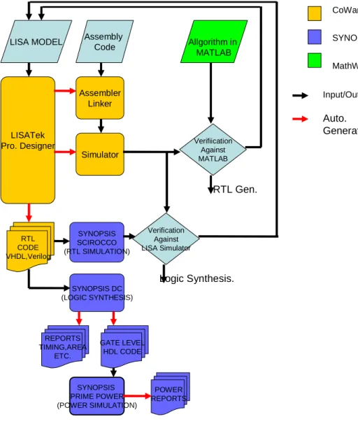
Figure 2.2 shows the design flow used in the thesis. The LISATek Processor Designer takes the model in LISA as the input, and generates the software tool chain, the assembler, linker and instruction set simulator automatically. The algorithm is written in the assembly language of the processor designed, and is simulated on the ISS and the results are verified against a high-level software implementation of the algorithm, Matlab. After verifing the correctness of the implementation of the processor and the algorithm in the assembly, the LISA model is converted to the Register-Transfer-Level (RTL) HDL code. LISATek
Processor Designer generates the VHDL code automatically from the LISA de-scription. Then the VHDL description of the processor is simulated on the SYN-OPSYS Scirocco simulation tool. LISATek tool suite has utilities to generate proper memory files to be used in VHDL simulation. Then the results of the simulation is verified against the ISS. The variable names used in LISA descrip-tion are kept similar while generating the VHDL code, i.e. the automatically generated HDL code is readable. After the verification of the processor’s VHDL description, the design is further synthesized into gate-level HDL description by Synopsis’ Design Compiler(DC) tool. At this step DC generates the timing and area reports. The gate-level description is then simulated on Synopsys’ Prime Power tool to get power reports.
SYNOPSIS MathWorks Auto. Generation LISA MODEL LISATek Pro. Designer Assembler Linker Assembly Code Allgorithm in MATLAB Simulator Verifiication Against MATLAB SYNOPSIS SCIROCCO (RTL SIMULATION) SYNOPSIS DC (LOGIC SYNTHESIS) RTL CODE VHDL,Verilog Verification Against LISA Simulator REPORTS TIMING,AREA ETC. GATE LEVEL HDL CODE SYNOPSIS PRIME POWER (POWER SIMULATION) POWER REPORTS CoWare Input/Output RTL Gen. Logic Synthesis.
Chapter 3
Cached FFT ASIP
3.1
The FFT Algorithm
The Discrete Fourier Transform of an N-point sequence is given by:
F (k) =
N −1X n=0
x(n) ∗ e(−j2π
Nkn) (3.1)
The DFT algorithm for an N-point sequence, requires N2 complex
multiplica-tions, i.e the complexity grows exponentially with the number of samples. The FFT algorithm breaks the N-point sequence into two N/2-point sequences and exploits the periodicity property of the DFT kernel e(−j2πNkn) to compute two
samples with just one complex multiplication instead of two. The two N/2-point sequences are further split into four N/4-point sequences and this procedure is repeated until getting 2-point sequences. At each step the number of multiplica-tions required is halved so that the complexity is reduced to N ∗ log2(N) (For a
derivation of FFT see[12]).
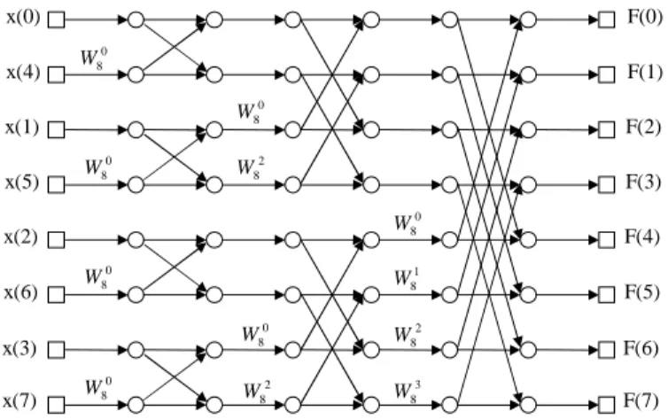
Figure 3.1 shows the flow graph of the radix-2 FFT algorithm. The computa-tion flow is from left to right. Each cross represents a FFT butterfly operacomputa-tion.
x(0) x(4) x(1) x(5) x(2) x(6) x(3) x(7) F(0) F(1) F(2) F(3) F(4) F(5) F(6) F(7) 0 8 W 2 8 W 0 8 W 2 8 W 0 8 W 1 8 W 2 8 W 3 8 W 0 8 W 0 8 W 0 8 W 0 8 W
Figure 3.1: Radix-2 FFT Flow-graph
The butterfly takes two complex inputs A and B and generates two complex outputs X = A + B ∗ W and Y = A − B ∗ W , where W is the twiddle factor:
Wk
N = exp(−j
2π
Nk)
The pseudo-code below shows the radix-2 FFT algorithm. It has two loops, one for counting the stages and one for counting the butterflies within the stages. For an N-point FFT, the number of stages is given by S = log2N and the number
of butterflies by B = N/2 for each stage.
FOR s=0 to S-1
FOR b=0 to N/2-1 BFLY(s,b) END
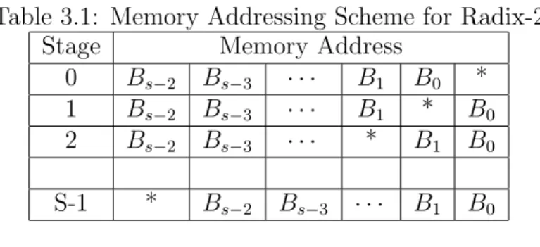
The BFLY(s,b) function in the above code, calculates the memory addresses of its two inputs from the loop variables s (stage number) and b (butterfly num-ber), performs a butterfly operation and saves the result back to the same mem-ory locations. The table below shows the memmem-ory addressing scheme for radix-2 FFT algorithm. Bits BS−2 to B0 are used to count the butterflies within a stage
and ’*’ is a place holder. Putting a ”0” in place of the ”*” gives the address of the input A (output X), and a ”1” gives the address of the input B (output Y). For every stage increment, the difference in the addresses between the two inputs of the butterfly is doubled.
Table 3.1: Memory Addressing Scheme for Radix-2 Stage Memory Address
0 Bs−2 Bs−3 · · · B1 B0 *
1 Bs−2 Bs−3 · · · B1 * B0
2 Bs−2 Bs−3 · · · * B1 B0
S-1 * Bs−2 Bs−3 · · · B1 B0
3.1.1
The Cached FFT Algorithm
The basic idea behind the cached FFT algorithm is to load part of the data from the main memory into a small cache and process as many stages of butterfly operations as possible without accessing to the main memory. Standard FFT algorithm reads the input data of the butterfly operations from the memory directly, therefore for an N-point FFT, the memory is read N ∗ log2N times,
since there are log2N stages. The cached FFT algorithm aims to decrease the
number of memory accesses by using a small cache and performing as many stages of computations as possible with the data in the cache, so that the factor
log2N is reduced.
The cached FFT algorithm can be derived from the FFT algorithm, by chang-ing the addresschang-ing scheme of the FFT algorithm. As shown in table 3.1, for a
stage increment the place holder ’*’ moves one to the left, in other words the only variable part is the bit position corresponding to the place holder. For P consecutive stages, the variable part becomes the P place holders. Since the idea is to compute P stages, the cache is loaded by fixing the other bits than these
P bits, and reading all the data corresponding to these 2P memory locations.
Table 3.2 shows the memory addressing scheme for the standard FFT algorithm, and table 3.3 shows the cached FFT algorithm’s cache loading scheme for N=64 point transform. It is desired to calculate P=3 consecutive stages with a cache of size 2P = 8. For the first three stages the place holders forms the 3 least
sig-nificant bit positions of the memory addresses, hence the 8-sized cache is loaded with the data corresponding to these 3 LSB positions, the remaining bits, the 3 most significant bits are held constant and are called the group bits. Once the cache is loaded with these data, the first three stages of butterfly computations can be performed. For the last three stages, the place holders form the three MSB positions, hence the data corresponding to these positions must be loaded, while keeping the 3 LSB as group bits. Group bits are so called because the whole data, N points must be processed in blocks of size C; the size of the cache, thus there are N/C groups.
Table 3.2: Memory Addressing Scheme for 64-point FFT Stage Memory Address
0 B4 B3 B2 B1 B0 * 1 B4 B3 B2 B1 * B0 2 B4 B3 B2 * B1 B0 3 B4 B3 * B2 B1 B0 4 B4 * B3 B2 B1 B0 5 * B4 B3 B2 B1 B0
Table 3.3: Cache Loading for 64-point FFT Stage Memory Address First Three Stages G2 G1 G0 * * *
Last Three Stages * * * G2 G1 G0
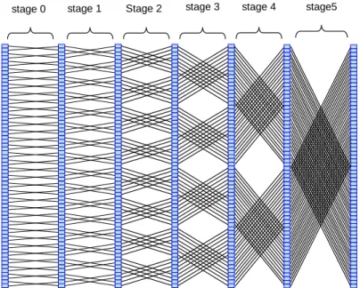
The FFT and cached FFT algorithms can be best visualized by their flow-graphs, figure-3.2 shows the simplified flowgraph of the standard FFT algorithm,
and figure-3.3 shows the flowgraph of the cached FFT algorithm. The transform length is N = 64, and the cache size is C = 8. With C = 8, three stages can be computed, since there are 6 stages, the transform is divided into two superstages called epochs. Within an epoch the cache is loaded and dumped back N/C times, i.e there are N/C goups in an epoch.
stage 1 Stage 2 stage 3 stage 4 stage5 stage 0
Figure 3.2: 64-point FFT Algorithm
The address calculations can be summarized as follows:
1. Having a cache of size C, log2C stages can be computed at most with the
data in the cache. Since there are log2(N) stages to compute, there are
e = log2N/log2C superstages, called epochs. In order to have a balanced
cached FFT algorithm, e must be an integer.
2. Within an epoch, the data is processed in groups. A group is a block of data in the memory, whose size is equivalent to cache size.Table 3.3 shows the cache loading and dumping for N=64 points cached FFT algorithm and e=2. The difference in cache loading and dumping for different epochs comes from the FFT addressing scheme. Since there are N data points in
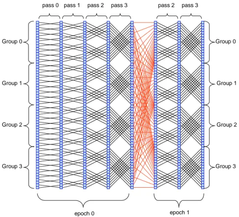
pass1 pass 2
pass 0 pass 0 pass 1 pass 2
epoch 0 epoch 1 Group 0 Group 1 Group 2 Group 3 Group 4 Group 5 Group 6 Group 7
Figure 3.3: 64-point Cached FFT Algorithm
the memory and the group size is C,there are N/C groups. In other words the cache must be loaded and dumped N/C times for each epoch.
3. Within a group, the data is processed in log2(C) stages which are called
passes. The data in the cache is addressed as shown in Table 3.4 4. Within a pass, C/2 butterfly operations are performed.
Table 3.4: Cache and twiddle addressing Epoch Pass Cache Index Twiddle Address
0 0 B1 B0 * 0 0 0 0 0 1 B1 * B0 B0 0 0 0 0 2 * B1 B0 B1 B0 0 0 0 1 0 B1 B0 * G2 G1 G0 0 0 1 B1 * B0 B0 G2 G1 G0 0 2 * B1 B1 B1 B0 G2 G1 G0
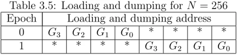
For some N, C is not an integer. In this case the algorithm becomes an Unbalanced-Cached FFT algorithm [2]. Unbalanced Cached FFT is calculated by first constructing the Cached FFT algorithm for the next longer transform length and removing some of the groups and passes from the calculation. For example, for 128-point FFT, the next longer transform length is 256. For 256-point FFT, the cache size is 16 for 2 epochs, and the number of groups is 16. Table 3.5 shows the cache loading and dumping for 256-point FFT.
Table 3.5: Loading and dumping for N = 256 Epoch Loading and dumping address
0 G3 G2 G1 G0 * * * *
1 * * * * G3 G2 G1 G0
For a 128-point FFT, the number of groups is 8, therefore 8 groups must be removed from the calculation as shown in Table 3.6.
Table 3.6: Loading and dumping for N = 128 Epoch Loading and dumping address
0 G2 G1 G0 * * * *
1 * * * * G2 G1 G0
The next step is the removal of the pass(es) from the calculation. There are 8 stages for a 256-point FFT and 7 stages for a 128-point FFT. Therefore, one pass must be removed from the calculation. The pass that must be removed from the calculation can be determined from Table 3.6. As highlighted in the Table, either the 3rd pass from epoch 0 or the 0th pass from epoch 1 can be removed (the pass corresponding to the overlapping placeholder ’*’).
The ASIPs that are presented in this thesis have support for both the balanced and unbalanced cached FFT.
3.1.2
The Modified cached FFT Algorithm
For a variable length implementation of the cached FFT algorithm, the size of the cache is determined by the largest possible number of points. Smaller size FFTs use a part of the cache only, so that the latter is only partially utilized. However, it is possible to change the structure of the algorithm to fully exploit the cache. This is achieved by computing more stages in epoch 0, rather than evenly distributing the stage computation in the two epochs. The parameters of the modified cached FFT algorithm for the 2 epochs are determined as follows:
• The number of butterflies in a pass is given by C/2, where C is cache size. • The number of passes for the two epochs is given by log2C and log2N −
log2C for epoch 0 and 1 respectively, where N is the number of FFT points.
• The number of groups is given by N/C.
In this case, C is given by Cmodif ied =
√
Nmax, rather than Coriginal =
√ N.
Since Cmodif ied > Coriginal for lower size FFT, less number of groups are required
because of the larger number of butterflies in a pass. Consequently, the number of cache loading and dumping is reduced.
For example, for a 64 point FFT (Figure 3.4), there are 6 stages, and
Coriginal = 8. If Nmax = 256, Cmodif ied = 16, the number of groups is 4, and
Group 1
pass 0 pass 1 pass 2 pass 3 pass 2 pass 3
Group 0 Group 3 Group 1 Group 2 Group 0 Group 2 Group 3 epoch 0 epoch 1
Figure 3.4: Modified Cached FFT Algorithm
3.2
Architectures for the Cached FFT
Algo-rithm
In this section, a Single Instruction Single Data (SISD) and a Very Large In-struction Word (VLIW) processor architecture for the CFFT algorithm are pre-sented. The basic instruction-set for the two architectures is the same. In both processors, the registers are used as caches. Since the size of FFT that can be implemented depends on the size of the cache and the number of epochs, a cache size of 32 and 2 number of epochs is selected. Therefore, the processors can compute FFT up to 1024 points according to the equation
C = NE1
where C is the cache size, N is the number of points and E is the number of epochs.
3.2.1
Instruction-Set Design
Below is a pseudo-code for the Cached FFT algorithm. It has 4 nested loops. For each group, the cache registers of the processor are filled with data from the memory, stages of butterfly operations are performed and finally the results in the cache registers are saved back to the memory.
FOR e = 0 to E-1 FOR g = 0 to G-1 Load_Cache(e,g); FOR p = 0 to P-1 FOR b = 0 to NumBFLY-1 Butterfly(e,g,p,b); END END Dump_Cache(e,g); END END
The kernel operation in the FFT algorithm is the butterfly operation which is composed of a complex multiplication followed by one addition and one sub-traction. In order to have a fast processor, cycle consuming operations must be optimized. This can be done by combining the whole instructions required to perform a butterfly computation into a single instruction [13]. Combining several instructions into a single instruction does not mean to execute every arithmetic operation in a single clock cycle, depending on the number of arithmetic opera-tions to be performed and data dependency between the arithmetic operaopera-tions the pipeline of the processor is made deeper. So that, several butterfly operations could be active on different pipeline stages. Both SISD and VLIW processors have a special BFLY instruction which not only performs the butterfly operation
but also calculates the cache register indexes and the twiddle coefficient address. The twiddle coefficient is precalculated and stored to a ROM, an alternative method to calculate twiddle coefficient by using CORDIC[14] is not considered since the precision of the coefficients worsen as the the number of CORDIC it-erations decrease, and using several cordic itit-erations could make the processor larger and slower. A VLSI implementation of the cached FFT algorithm by em-ploying the CORDIC machine has already been proposed in [15] The cache index and memory address calculations require
1. The total number of passes, groups and butterflies. These 3 parameters together with the number of bit reversing are specified in a 16-bit control register (CTR)
2. The group, pass, butterfly and the epoch numbers for a given iteration. The first three parameters are passed with general purpose registers whereas the epoch number is passed as a 2 bit immediate value.
The latter means that the outermost loop for the epoch is unrolled. The BFLY instruction has an automatic post-increment addressing mode. Figure 3.5 shows the structure of the instruction.
Several approaches can be used to speed-up the execution of loops. The simplest one is the delayed branch technique, where some instructions following a conditional branch are always executed, regardless of whether the branch is taken. This technique was not considered for the two cached FFT ASIPs because, in our implementation, the core of the loop consists of the single BFLY instruction. A more sophisticated technique is Zero-Overhead-Loop (ZOL) that enables efficient implementation of loops. The programmer specifies which instructions have to be repeated and how many times, then the processor automatically manages the loop index and terminates the loop accordingly. The concept of ZOL can be extended to nested loops with a further speed improvement at the expense
Figure 3.5: Structure of the BFLY instruction
of increased hardware complexity [16]. This complexity can be avoided for the cached FFT algorithm by using a simple RPT instruction as shown below.
For loading data from the memory into the cache registers, a READ instruc-tion was added. The instrucinstruc-tion uses 2 pointers: Read Pointer (RP) for indexing the memory and Cache Pointer (CP) for indexing the cache registers. The READ instruction loads data from memory addressed by RP into the cache register in-dexed by CP. It also automatically increments the CP, and takes the number of increment for RP as an immediate operand. The code below shows how 32 data words are loaded into the cache registers and the butterflies computed.
RPT #32 READ #1 RPT #16
Both RP and CP are dedicated registers, and can be initialized by special in-structions.
For decimation in time, the memory address specified by RP must be bit reversed. The number of bit reversing is equal to log2N, an is specified in the
control register CTR. For dumping the cache into the memory, there is a WRITE instruction which is similar to the READ instruction.
3.2.2
The SISD Architecture
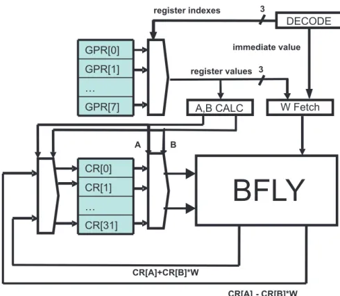
This is a load-store architecture with 6 pipeline stages: fetch, decode and 4 execution stages. There are 8 general purpose registers in addition to the 32 cache registers and 12 special purpose registers. The latter are used for addressing and for flow control. There are 3 memories for program, data and coefficients with the configurations 24x256, 32x1024 and 32x512 respectively. The 16-bit real and imaginary parts of a data or coefficient are concatenated to form a 32-bit word. Figure 3.6 shows the structure of the pipeline.
The stages EX2 to EX4 are used by the BFLY instruction only. The execution of this instruction proceeds as follows: in EX1 stage, the 4 operands of the BFLY instruction are used to calculate cache register indexes and the twiddle address according to table 3.4. The twiddle is then fetched from the dedicated twiddle memory. In the following two stages, a complex multiplication between the second input sample and the twiddle factor is performed. Four parallel multiplications are computed in one stage, followed by two parallel additions in the other. In the final pipeline stage, the results calculated in the previous stage are added to and subtracted from the first input sample to calculate the 2 outputs of the butterfly, and the results are then saved to the respective cache registers.
3.2.3
The VLIW Architecture
This is also a load-store architecture with 4 slots, each of which can execute a BFLY instruction (figure 3.7). The BFLY instruction is similar to the one in the SISD architecture with the difference that the execution occurs in 3 rather than 4 stages. In this case, the last 2 operations in the BFLY are done in one stage. The reason is that, in the former case, the BFLY instruction takes its inputs in the 3rd
pipeline stage and outputs the result in the 6th. For the SISD architecture, the
BFLY instructions are executed sequentially, and there is no data hazard between the passes. However, for the VLIW case, 4 BFLY instructions are executed in parallel and there are data hazards between the passes due to pipelining. In order to reduce this problem, the last two pipeline stages are combined so that the results of the BFLY instructions are available earlier. An alternative solution of using a forwarding mechanism is not considered for this architecture. Such a mechanism would result in a significant area increase, since each of the 8 outputs could potentially go into any of the 8 inputs.
Combining the last two stages does not completely resolve data dependencies. For the same reasons as above, interlocking was not implemented. Instead, since the code size is rather small, the problem is resolved in the assembly source by inserting NOP instructions between the passes. The trade-off is acceptable in this case because there is a maximum of 7% increase in total number of cycles for N = 256. For N > 256, there are no data dependency problems between the passes. For N < 256, the increase in number of cycles is lower. It is worth to mention that, there is no data hazard for modified CFFT algorithm, since the cache is fully utilized valid instructions are inserted instead of NOP instructions. Since 4 butterfly instructions execute in parallel, and since they need 4 dif-ferent twiddle factors for some passes, the twiddle coefficient memory is divided into 4 physically separate memories, each with the configuration 32×128. Each slot of the VLIW architecture has access to every of the 4 twiddle memories. Ex-pensive interleaving is not necessary because access conflicts can be completely avoided in software if the architecture is carefully designed. Table 3.7 shows the twiddle addressing scheme for the VLIW architecture. The most significant 2 bits are used to select the twiddle memory. The 2 bits are in turn determined by the group, pass, epoch and the butterfly number. In any iteration, the former 3 numbers are the same. Therefore, selecting butterfly numbers having a difference of 4 guarantees that there is no conflict for all passes. The code below show how this is achieved for N=64 for epoch 0 (The VLIW for modified CFFT).
BFLY R[0],R[1],R[2]++,#0 || \ BFLY R[0],R[1],R[3]++,#0 || \ BFLY R[0],R[1],R[4]++,#0 || \ BFLY R[0],R[1],R[5]++,#0
The registers R[2],R[3],R[4] and R[5] which contain the butterfly numbers are initialized to 0, 4, 8 and 12 respectively prior to each group iteration.
Figure 3.7: The VLIW Architecture showing the BFLY
Table 3.7: Twiddle Addressing Scheme for the VLIW ASIP E Pass Twiddle Coefficient Address
0 0 0 0 0 0 0 0 0 0 0 1 B0 0 0 0 0 0 0 0 0 2 B1 B0 0 0 0 0 0 0 0 3 B2 B1 B0 0 0 0 0 0 0 4 B3 B2 B1 B0 0 0 0 0 0 1 0 G4 G3 G2 G1 G0 0 0 0 0 1 B0 G4 G3 G2 G1 G0 0 0 0 2 B1 B0 G4 G3 G2 G1 G0 0 0 3 B2 B1 B0 G4 G3 G2 G1 G0 0 4 B3 B2 B1 B0 G4 G3 G2 G1 G0 | {z } | {z }
Selects the Selects the cell within the twiddle
Chapter 4
Cached Fast Hartley Transform
ASIP
4.1
The Fast Hartley Transform Algorithm
For an N-point sequence x(n), 0 < n < N − 1, the DHT [4] is given by:
H(k) =
N −1X n=0
x(n)cas(2π
N kn) (4.1)
and its inverse is given by:
x(n) = 1 N N −1X k=0 H(k)cas(2π Nkn) (4.2)
Where cas(x) = cos(x) + sin(x). As seen in the equations, the same cas function is used for both forward and inverse transforms. This feature of DHT is especially valuable for an hardware implementation, since the same hardware can be used for both transforms. FHT[7] is derived from DHT in the same way
FFT is derived from DFT (for a detailed derivation of FHT see[17]). The N point sequence is first divided into two N/2 sequences:
H(k) = N/2−1X n=0 x(2n)cas(2π N2kn) + N/2−1X n=0 x(2n + 1)cas(2π N (2n + 1)k) (4.3)
Now, the idea is to calculate H(k) which is the DHT of x(n), from H1(k) and
H2(k), which are the DHTs of x1(n) = x(2n) and x2(n) = x(2n + 1) respectively.
Apparently the first term in the above equation is the DHT of x1(n) which is
H1(k), but the second term is not the DHT of x2 since the cas function in the
second term is not a valid DHT kernel, due to a time shift. By using the shift rule of DHT given below:
H(k + c) = cos(c)H(k) + sin(c)H(−k) (4.4) it can be shown that the second term in equation (4.3) is equal to:
cos(2π
N k)H2(k) + sin(
2π
Nk)H2(−k) (4.5)
finally H(k) can be rewritten in terms of H1(k) and H2(k) as:
H(k) = H1(k) + cos(
2π
Nk)H2(k) + sin(
2π
Nk)H2(−k) (4.6)
Above equation is valid for 0 ≤ k ≤ N/2 − 1. To calculate H(k) for k ≥ N/2, the periodicity of the DHT and the symmetry of the cas function can be used. DHT of a sequence is periodic with the sequence length, that is:
And the cas function is:
cas(2π
N(n + N/2)) = −cas(
2π
Nn) (4.8)
Now the complete formula for the computation of H(k) is:
H(k) = H1(k)+ cos(2π Nk)H2(k)+ sin(2π Nk)H2(−k) 0 ≤ k ≤ N2 − 1 H1(k −N2) −cos(2π N(k − N2))H2(k −N2) −sin(2π N(k −N2))H2(−k + N2) N2 ≤ k ≤ N − 1 (4.9)
The switching from DHT to FHT lies in equation (4.9). The right hand side of the above equation contains inputs which are the same for the two equations due to periodicity. Therefore two H(k) can be calculated together, for instance
H(0) and H(N/2). Thus, by dividing the sequence into two smaller sequences,
the complexity of DHT is reduced. The splitting procedure can be repeated until we get 2 point sequences. The FHT algorithm can be best understood by its flow graph. Figure 4.1 shows the structure of the FHT for Decimation-In-Time approach[18]( A complete set of other approaches, decimation-in-frequency, radix-4 etc can be seen in[19]). The 16-length sequence x(n) is split into two smaller sequences successively. This procedure can be seen on the graph (from right to left). Since for each splitting the sequence is split into even and odd indexed sequences, the x(n) sequence shows in a permuted order. The signal flow, so the computation flow, is from left to right, when signals are transmitted by unbroken lines their values remain unchanged. If a signal is transmitted by a broken line, its sign is reversed. The internal structures of blocks T3 at level 3 and T4 at level 4 are shown on the bottom of figure 4.1. Multiplications with
cosine and sine functions are performed in these blocks. Apparently for the first two blocks cosine and sine functions give 1 or 0 as the result. So there are no T blocks for the first two stages.
Figure 4.1: FHT Flow Graph
4.1.1
Structure Of The FHT Algorithm
In terms of data addressing scheme, FHT flow graph is exactly the same of FFT except the T blocks. In FHT algorithm, a butterfly has two inputs one of which is directly connected to the previous stage and the other one is connected through the T block. An output of T block is a function of two inputs of the T block. Therefore a butterfly needs one additional input due to the T block, thus 2 output values are calculated by using 3 input values. This input-output inefficiency can
be avoided by calculating another butterfly which shares the two inputs of the first butterfly and needs one additional input, thus by using 4 inputs, 4 outputs can be calculated (Dual butterfly) [20]. Since a dual-butterfly has 4 inputs, there are N/4 dual-butterflies in a stage. It should be noted that for the first two stages, there is no T block; hence the butterflies can be independently computed.
4.1.2
Memory Addressing
Table 4.1: Memory Addressing For FHT Stage Memory Address
1 B4 B3 B2 B1 B0 X * 2 B4 B3 B2 B1 B0 * X 3 B4 B3 B2 B1 * 0 B0 4 B4 B3 B2 * 0 B1 B0 5 B4 B3 * 0 B2 B1 B0 6 B4 * 0 B3 B2 B1 B0 7 * 0 B4 B3 B2 B1 B0
Table 4.1 shows the memory addressing scheme of the FHT algorithm. For the first two stages, there is no need for dual- butterfly computation, since the individual butterflies are independent from each other. For the remaining stages, the aim is to count the dual-butterflies. Since a dual-butterfly involves 2 but-terflies and since the addresses of these two butbut-terflies are interrelated by the T block, we can count only one butterfly of the dual-butterfly and derive the address of the other from the address of the first one. For this purpose, one of the bits is set to 0 in table 4.1. By doing so, the addresses of the inputs corre-sponding to upper half (graphically upper) of the T blocks are calculated. A ”0” in place of ”*” gives the address of the input which is not in the T block (X0), a ”1” in place of the ”*” gives the address of the input which is in the upper half of the T block (X1). The dual-butterfly needs two more addresses. If IndexX is the digits right to the ”*”:
IndexY =
2stage−1− IndexX IndexX 6= 0
2stage−2 IndexX = 0
(4.10)
Now the remaining two addresses for the second butterfly can be calculated by concatenating bits left to the ”*” with IndexY. These two addresses are Y0 (a ”0” in place of the ”*”) and Y1 (a ”1” in place of the ”*”)
4.1.3
Dual-Butterfly Computation
Having calculated the 4 addresses, the next step is the computation of the dual-butterfly:
M [X0] = M [X0] + (M [X1]cos(φ) + M [Y 1]sin(φ)) (4.11a)
M [X1] = M [X0] − (M [X1]cos(φ) + M [Y 1]sin(φ)) (4.11b)
M [Y 0] = M [Y 0] + (−M [X1]cos(φ) + M [Y 1]sin(φ)) (4.11c)
M [Y 1] = M [Y 0] − (−M [X1]cos(φ) + M [Y 1]sin(φ)) (4.11d)
where φ = IndexX2π
2stage
The second terms in the right hand side of above equations are actually the computations in the T blocks. Apparently for IndexX=0, above computations reduce to additions and subtractions.
4.2
Cached Fast Hartley Transform Algorithm
The idea behind the cached FHT algorithm is to load part of the data from memory into a cache and process as many stages of butterfly computations as possible by using the data in the cache. The cached FHT algorithm can be
derived from FHT in a manner similar to cached FFT is derived from FFT algorithm [2].
4.2.1
Derivation of Cached FHT Algorithm
The difficulty in cached FHT algorithm is the additional data dependency caused by the T blocks. To derive cached FHT, we first show an example and then generalize the cached FHT algorithm. For N = 128, there are 7 = log2(N)
stages and if we have a cache of size 16 (C=16). The first 4 (log2(16)) stages can
be calculated without a problem, since all the addresses of the four inputs of a dual-butterfly lie in 16-size page. So, the cache can be loaded for 8 groups as in table 4.2, and four each group, 4 stages of dual-butterfly computations can be
Table 4.2: Cache Loading For The First Epoch Memory Address Cache Address
g2 g1 g0 * * * * * * * *
performed. At the end of the computations the results in the cache are dumped back to the memory for each group. This constitutes the first epoch. For the second epoch, there are 3 stages of computations remaining. For these 3 stages, the cache must be so loaded that all the data for the 3 stages must be available in the cache. Since the FHT is similar to FFT except the T blocks, half of the cache must be loaded as in the cached FFT and the other half is loaded by considering T block dependencies.
Table 4.3: Cache Loading For The Second Epoch Memory Address
B4 B3 * 0 B2 B1 B0
* * * 0 g2 g1 g0
* * * 1 ag2 ag1 ag0
The first row in table 4.3 shows the butterfly addressing scheme for the stage 5. As explained previously these butterflies correspond to the upper half of the T
blocks for stage 5. For further stages, the * moves toward left. Since the aim is to calculate stages of butterfly computations with the data in the cache, the cache must be loaded for variable part, which are the addresses corresponding to 3 Most Significant Bit (MSB) positions, while keeping the 4 Least Significant Bit (LSB) positions constant. So half of the cache is loaded from the memory locations given in the second row of table 4.3. The remaining half of the cache must be loaded by considering the T block dependencies. For the group, G = g2g1g0 = 001,
and for all butterflies in stage 5, IndexX will be 0001 therefore , IndexY=1111 (IndexY = 2stage−1− IndexX), thus for G=001 we need to load remaining half
of the cache with another group AG =111 (auxiliary group) as in the third row of table 4.3. Now lets investigate if the same data in the cache can be used for stage 6. Since G=001, IndexX will be either 00001 or 10001 depending on the butterflies in the stage 6, consequently IndexY will be either 11111 or 01111 respectively, since the 3 LSB of IndexY is 111 the data is available in the auxiliary cache. Similarly for stage 7 IndexX will be 000001, 010001,100001, 110001 and correspondingly IndexY 111111, 101111, 011111, 001111 again the 3 LSB of IndexY is 111. So the data required for 3 stages of computations can be loaded into the cache. This procedure can be repeated for other groups(G), the auxiliary group(AG) is determined from G as follows:
AG = 2log2(C)−1− G G 6= 0 0 G = 0 (4.12)
where C is the size of the cache. Having loaded the cache with the data, the next step is to calculate the addresses of the data in the cache for each pass and butterfly. As assumed, the least significant half of the cache contains the data corresponding to upper half of the T block for the first pass. These cache addresses can be found from the left hand side of table 4.4. And the data corresponding to lower half of the T blocks lie in the most significant half of the
cache and they can be found by the right hand side of table 4.4. In this table, the ”-” represent a binary inversion and it is due to IndexY calculation.
Table 4.4: Cache Addressing
Pass Cache Address For G Cache Address For AG 0 0 B1 B0 * 1 B1 B0 *
1 0 B1 * B0 1 B1 * −B0
2 0 * B1 B0 1 * −B1 −B0
The final step is to compute the address of the cas function. For the FHT algorithm it is equivalent to the IndexX, so for the cached FHT it is calculated by concatenating digits right to the ”*” of the cache address for G and group digits. It should be noted that for the group G=0, AG is also 0, so the cache loading and cache indexing must be done as in the first epoch.
4.3
Processors For The FHT Algorithm
We have designed two Application Specific Processors for the FHT algorithm. The first processor is implemented for the FHT algorithm and the second one for the cached FHT algorithm. Both processors have 16 bit data path, and a special ”dual-butterfly” instruction.
4.3.1
FHT Processor
FHT algorithm requires four data for the dual-butterfly computation, the natural solution is to use a 4-ported memory, but the energy dissipation and the die area of a 4-ported memory is not feasible, so we have used a dual-ported memory with a pipeline interlocking mechanism. Figure-4.2 shows the pipeline struc-ture of the FHT processor. In the first two pipeline stages, the instructions are
fetched from program memory and decoded. If the decoded instruction is ”dual-butterfly” instruction, the 4 addresses are calculated from the operands of the ”dual-butterfly” instruction in the 3rd pipeline stage together with the address
of the cas function. In the 4th pipeline stage, two memory locations are loaded
corresponding to IndexX, in the 5th pipeline stage, two data for the IndexY are loaded from memory and previously loaded two data are multiplied by respective sine and cosine values (see eqns 4.11a and 4.11b). In the remaining stages dual butterfly computation is completed. As it is noticed from pipeline figure, two pipeline stages have access to the memory, if two consecutive instructions have memory accesses, a data hazard arises. In order to solve this problem, pipeline interlocking mechanism is used. In the DE and ADR stages of the pipeline the processor determines whether both instructions have memory access and stalls the pipeline if it determines a data hazard.
FE
DE
ADR
MEM
MEM
&
MUL
ADD
ADD
&
SUB
Multiplex.
Dual-port
Data
memory
Single-port
Coefficient
memory
Figure 4.2: FHT PipelineAt the final pipeline stage, the dual-butterfly computation is completed and the results are saved to the registers of the processor. The processor has 32 data and address registers, therefore after executing 8 dual-butterfly instructions
the registers are filled completely and the results are saved to the memory by executing 16 ”store” instructions.
4.3.2
Cached FHT Processor
The cached FHT processor has 64 registers for the purpose of caching. The processor can compute up to 2048 point FHT, 6 passes in the first epoch and 5 passes in the second epoch. Figure 4.3 shows the pipeline structure of the processor. This processor loads the two blocks corresponding to the group and the auxiliary group bits to the cache and auxiliary cache registers and performs dual butterfly operations on these cache registers. Since the 4 operands of the dual-butterfly operation comes from cache registers, one of the memory accessing stages of the FHT algorithm does not exist in the cached FHT processor. This processor also has a dual-ported data memory and the cache is loaded from the memory by means of two read pointers, one of which is for the G (group) and the other one is for AG (Auxiliary Group). After the cache is loaded with data, dual-butterfly computations are performed. Since ”dual-dual-butterfly” operation requires 4 data from the cache registers, both cache and auxiliary cache registers are 8-ported, 4 port for reading and 4 port for writing. The cached FHT processor has support for two epochs only, and the assembly code for the two epochs are unrolled, since the cache loading and dumping for the two epochs are different.
FE
DE
ADR
MEM
ADD
ADD
&
SUB
Dual-port
Data
memory
1-port
Coeff-memory
Program
memory
Cache
Registers
Aux.
Cache
Registers
Figure 4.3: FHT PipelineChapter 5
Results and Conclusion
This thesis aimed at designing and implementing low power, flexible FFT pro-cessors for the European Union funded NEWCOM OFDM project. Several al-gorithms are explored by the researchers from Technical University of Aachen, Politecnico di Torino and Bilkent University. The cached FFT ASIP is chosen as the processor for the project due to its low power consumption. All of the processors compared in the following sections are ASIPs. The ASIPs designed in this thesis are not compared with ASIC processors, since such a comparison is unfair. All of the processors compared in the next section are designed with the same design methodology [9] and synthesized with the same technology library; UMC 0.13µ.
5.1
Implementation Results for cached FFT
ASIP
CFFT-S is the SISD ASIP that was described in Section 3.2.2. For a comparison with the Cooley-Tukey(CT) algorithm, the ASIP which is described in [16] is
considered. In that publication, the authors describe two ASIPs with an opti-mized data-path and with an optiopti-mized control-path respectively. The former is selected for comparison because this ASIP is comparable to CFFT-S: both con-tain a butterfly instruction which fetch the operands and update the addresses with a minimum overhead. However, the data path optimized ASIP, which is here called CT-D (CT is an abbreviation for Cooley- Tukey FFT algorithm), does not have instructions for ZOL as is the case with CFFT-S. Since this com-parison aims at determining the reduction in energy dissipation as a consequence of less number of accesses to the main memory, a direct comparison with CFFT-S would be inconclusive. Therefore, an ACFFT-SIP CT-Z which is similar to CT-D, but which supports nested ZOLs was implemented by our research partners from VLSI lab of POLITO[21] and Institute of Integrated Systems, RWTH, Aachen [22]. The selected technique for nested ZOLs is the same as in [16]. The by-pass mechanism of CT-D was not re-implemented in CT-Z. This is because the CT-FFT algorithm can be similarly implemented on CT-Z without any need for bypassing. Energy Consumption 0 0.5 1 1.5 2 CFFT-S CT-Z CT-D Processors E n e rg y (u J ) 256 point 1024 point