*Correspondingauthor, e-mail:[email protected]
Journal of Science
http://dergipark.gov.tr/gujsInterface Effects of Annealing Temperatures in Al/HfO
2/p-Si (MIS)
Structures
Şadan ÖZDEN1,*, Osman PAKMA2
1Department of Physics, Faculty of Science, Muğla Sıtkı Koçman University, 48000, Muğla, Turkey 2Department of Physics, Faculty of Science and Art, Batman University, 72100, Batman, Turkey
ArticleInfo Abstract
In this study, Al/HfO2/p-Si (MIS) structures were prepared by using the sol-gel method for three
different annealing temperatures. The current-voltage (I-V) and capacitance-voltage (C-V) characteristics of these structures were investigated by taking into consideration the effect of the interfacial insulator layer and surface states (Nss) at room temperature. All of the structures
showed non-ideal I-V behaviour with ideality factor (n) in the range between 2.35 and 4.42 owing to interfacial insulator layer and surface states. The values of Nss and barrier height (b) for three
samples were calculated. The values of n and Nss ascend with increasing the insulator layer
thickness (δ) while the values of b decreases.
Received: 26/03/2017 Accepted: 25/05/2017 Keywords High dielectric materials, sol-gel, MIS devices 1. INTRODUCTION
Metal-semiconductor (MS) and metal-oxide-semiconductor (MOS) diodes are of great importance for contributing to the understanding of the semiconductor surface and surface states. Any insulator layer, produced between metal and semiconductor by means of the natural or deposition process, causes the metal-insulator-semiconductor (MIS) diode having non-ideal behavior. Thus, the “ideality factor (n), surface states (Nss), and barrier height (b) of an MIS structure significantly differ from the expected magnitudes, which is mainly caused by the potential drop across the insulate layer due to the interface states at insulator/Si interface [1-7]. Recently, the growth of various insulators on single crystalline silicon, such as SnO2 [8], Si3N4 [9], TiO2 and hafnium dioxide (HfO2) [10-11], in MIS structures has been subject to extensive research as an alternative to silicon-dioxide (SiO2). The small number of surface states, high dielectric permittivity and high breakdown voltage are among the important advantages of these films when compared to SiO2. MIS diodes produced by HfO2 thin films are also of considerable importance due to the same advantages.
HfO2 is one of the most common and stable compounds of hafnium. Therefore HfO2 is used in optical coatings, and as a high-κ dielectric in DRAM capacitors and in advanced metal-oxide-semiconductor devices [12]. In view of the these facts, the experimental investigations on Al/HfO2/p-Si (MIS) structures prepared by the sol-gel method at three different preparation temperatures have been carried out and their main electrical parameters such as b, n and Nss have been investigated by taking into account the effect of the interfacial insulator layer. To explain the forward bias I-V and C-2-V characteristics, the model provided in literature has been used [3-6].
2. EXPERIMENTAL
2.1. Al/HfO2/p-Si Structures Preparation
To prepare the HfO2 solution, 0.0063 mol hafnium tetrachloride was dissolved in 15 mL ethanol, to which 0.08 mol H2O and 0.013 mol HNO3 were added and the solution was kept in a magnetic stirrer for 2 hours. Finally, before coating the film, the solution was maintained at 50 °C for 4 hours.
Metal-oxide-semiconductor (Al/HfO2/p-Si) structures were manufactured on the 1-inch diameter float zone (100) p-type (boron-doped) single crystal silicon wafer with a thickness of 280 μm and a resistivity of 1– 10 Ω.cm. For the fabrication process, Si wafer was degreased through the RCA cleaning process (i.e., a 10 minute boiling in NH4OH + H2O2 + 6 DI (18 MΩ deionised water), which was followed by a 10 minute boiling in HCl + H2O2 + 6 DI) [10, 13]. Then, it was subjected to the drying process in N2 atmosphere for a duration time. After that, high-purity aluminum with a thickness of 1500 was thermally evaporated from the tungsten filament onto the whole back surface of the Si wafer under the pressure of 10−6 Torr. In order to obtain a low-resistivity ohmic back contact, Si wafer was sintered at 580 °C for 3 minutes in N2 atmosphere. The native oxide on the front surface of the substrate was removed in HF : H2O (1 : 10) solution, and finally, the wafer was rinsed in deionised water for 30 s before forming an HFO2 layer on the p-type Si substrate. The prepared HFO2 solution was coated on the shiny side of the cleaned p-Si surface at 2000 rpm by the sol-gel spinning technique. The HfO2/p-Si structures were annealed for five minutes at 100, 200, and 300 °C in N2 atmosphere after each coating process. The process was repeated in the same way until the required film thickness was obtained and the structure was finally exposed to annealing at 500 °C in N2 atmosphere for 1 h.
Figure 1. Schematic diagram of Al/HfO2/p-Si (MIS) structure.
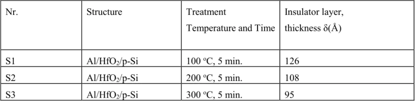
A high-purity aluminum layer (2000 Ǻ) was coated on the surface in a vacuum under the pressure of 10-6 Torr in order to obtain a rectifying contact on the front surface of p-Si coated with HfO2. The structure of Al/HfO2/p-Si/Al (MIS) structures is given in Figure 1. The preparation data of HfO2 thin films on Si wafer substrate are given in Table 1.
Table 1. Preparation data of HfO2 thin films prepared on Si wafer substrate.
Nr. Structure Treatment
Temperature and Time
Insulator layer, thickness δ(Å)
S1 Al/HfO2/p-Si 100 oC, 5 min. 126
S2 Al/HfO2/p-Si 200 oC, 5 min. 108
S3 Al/HfO2/p-Si 300 oC, 5 min. 95
Ohm11..
2.2. Characterization
The insulator layer thicknesses of prepared devices were measured by Avantes spectrometer (AvaSpec-ULS2048). The current-voltage (I-V) and capacitance-voltage (C-V) measurements, carried at 500 kHz with a test signal of 50 mVrms, were performed by Keithley-4200 semiconductor characterization system (SCS) at room temperature and in a darkened and sealed metal box, respectively.
3. RESULTS AND DISCUSSION
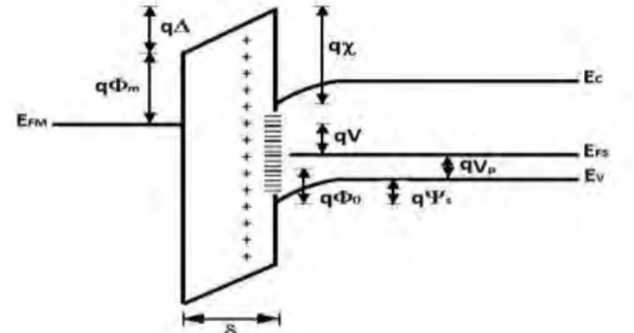
The energy band diagram of an MIS structure at forward bias is presented in Figure 2. The parameters m, χ, Δ and δ are the work function of metal, the electronic affinity of the semiconductor, the voltage drop
across the interface insulator layer, and the thickness of the insulator layer, respectively. The parameter 0
is commonly defined as the neutral level of surface states taken from the valance band edge at the semiconductor surface [14]. Vp is the potential difference between the Fermi level and the top of valence
band in the neutral region, and e is the effective barrier height.
Figure 2. The energy band diagram of a MIS system under non-equilibrium condition.
From the energy band diagram, the potential drop Δ across the interface layer can be determined by Gauss’s law [7, 14];
sc it f
i m e gQ
Q
Q
q
E
(1) where Qsc is the semiconductor depletion layer charge, Qit is the interface trap charge at bias V, Qf is thefixed surface charge at the semiconductor interface and i is permittivity of the insulator layer. The depletion charge is given by
2
(
)
1/2 n e A s scq
N
V
Q
(2)where NA is the doping concentration and s is the permittivity of semiconductor. The interface state charge
is:
)
(
q
q
0qN
Q
it
ss e
(3)where Nss is the density of the interface states. From the above equations, the following expressions can be
written as: 2 2 1 2q sNA / i c
(4a) ) /( 2 2 i i q Nss c
(4b) ) / ( ) / ( ) 1 ( ) / ( 2 0 2 2 2 g m f i b f i e c E q
c
c
Q
c
Q
(4c)where b is the barrier height without fixed surface charge at thermal equilibrium and can be defined by
0 2
2( /
) (1 )
b c Eg q m c (5)The depletion layer capacitance per unit area of a MS contact without interfacial layer can be given by
q
N
/
2
(
V
V
)
1/2C
s A d
(6) qE~M
---,
+ I + +~---
E
e
From equation (6), the quantity of C-2 can be written as A s d V q N V C2 2( )/
(7) When a metal-semiconductor contact with interfacial layer (MIS) is considered, the depletion capacitanceC can be become [2],
1/2 2 2 2q
sN
A/
2
bc
V
V
nc
(
Q
f/
i)
c
C
(8) and
bc
V
V
nc
Q
f i
c
q
sN
AC
2
2 2 2 2
2
(
/
)
/
(9)c2 can be written as follows from the slope of the C-2-V plot
A A sN
N
dV
C
d
N
q
c
A ' 2 2
(
2
)
/
(10)where N’A is the experimental value of doping concentration and NA is the theoretical value of doping
concentration. From the intercept of C-2-V plot with the voltage axis, the value of b can be obtained as
) / ( ) ( 2 0 n 2 f i b cV V c
Q
(11)From equations (6) and (11), the effective barrier height at thermal equilibrium may be defined as
)
(
2 0 n e
c
V
V
(12)where V0 is the intercept voltage. According to equation (11), the barrier height without the fixed surface
charge can be given by
)
(
2 0 n b
c
V
V
(13)In order to obtain b or e, from equations (12) and (13), it is necessary to known the Fermi energy Vn. From
equation (4b), the value of c2 is a function of δ and Nss.
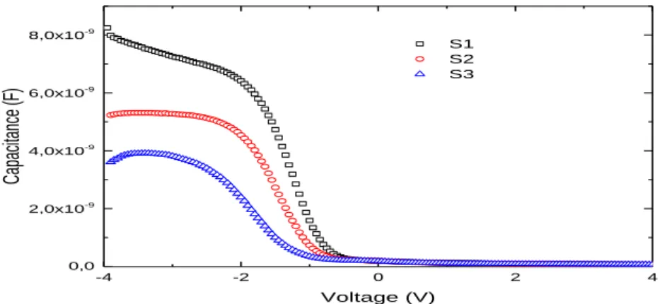
Capacitance-voltage (C-V) measurements are performed at a sufficiently high frequency (f ≥500 kHz) to prevent the interface states responding to the ac signal [15, 16]. Therefore, the forward and reverse bias
C-V characteristics at 500 kHz for three different annealing temperatures are shown in Figure 3. The applied
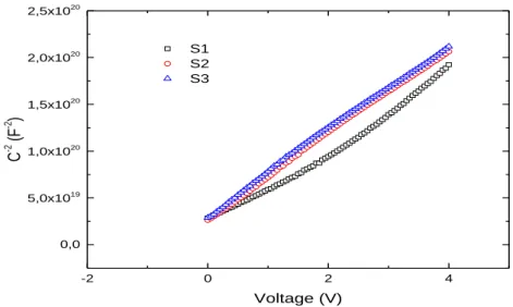
voltage was varied between -4 V and +4 V. From an MS or MIS structure, the doping density concentration (NA), and the diffusion potential (Vd) can be directly achieved from the slope and the intercept with the
voltage axis of C-2 vs. V plot [1, 2]. C-2 vs. V plots were shown in Figure 4. Values of N
A and c2 were
calculated for all structures according to Eq. (10) using the slope data obtained from C-2 vs. V plots.
-4 -2 0 2 4 0,0 2,0x10⁻⁹ 4,0x10⁻⁹ 6,0x10⁻⁹ 8,0x10⁻⁹ S1 S2 S3 Capa citan ce ( F) Voltage (V)
Figure 3. High frequency (500kHz) capacitance – voltage characteristics of Al/HfO2/pSi (MIS) structures
at room temperature.
Then the values of b were calculated, as the values of c2 and Vn are known. There is a linear correlation
between b and c2 as shown in Figure 5. From the extrapolation of the line to c2=1 the value of b was found
to be equal to 1.032 eV and also from the extrapolation of that to c2=0 the value of neutral level 0 of
surface states was obtained as 0.12 eV.
0
-2 0 2 4 0,0 5,0x10¹⁹ 1,0x10²⁰ 1,5x10²⁰ 2,0x10²⁰ 2,5x10²⁰ S1 S2 S3 C -2 (F -2 ) Voltage (V)
Figure 4. C-2-V characteristics for 500 kHz of the Al/HfO2/p-Si MIS structures at room temperature.
0,00 0,05 0,10 0,15 0,20 0,25 0,30 0,35 0,40 0,45 0,50 0,55 0,00 0,05 0,10 0,15 0,20 0,25 0,30 0,35 0,40 0,45 0,50 0,55 0,60 q b (eV) c2 c2=0 c2=1 b=0.12 eV b=1.032 eV
Figure 5.b - c2 plot of the Al/HfO2/p-Si MIS structures at room temperature.
Due to the existence of an insulator layer at M/S interface, it is assumed that there is a relation between the applied forward bias voltage V (V>3kT/q) and the current I. According to the thermionic emission (TE) theory, the current is expressed as [1],
kT N q qV I I i ss oexp (1 2
/
) (14) where I0 is the reverse saturation current and is given as
kT
q
T
AA
I
* 2exp
b 0 (15) whereb, A, A*, n, q and T are zero-bias barrier height, the rectifier contact area, the effective Richardsonconstant (32A/cm2K2 for p-type Si), ideality factory, the electron charge and the temperature in K, respectively. The value of 1+q2
ss/Ican be considered as the ideality factor of the MIS structure.
According to equation (4b), this factor should be equal to 1/c2.
•
0
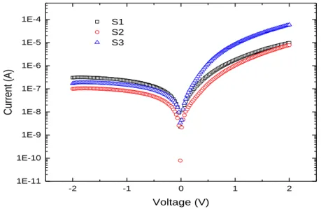
Figure 6 shows the forward bias lnI-V characteristics of Al/HfO2/p-Si (MIS) structures at the room temperature. The determined values of the ideality factor (n) range from 2.35 to 4.42. These values of n are appreciably high. Such behavior of ideality factor can be attributed to the interfacial insulator layer and interface states. -2 -1 0 1 2 1E-11 1E-10 1E-9 1E-8 1E-7 1E-6 1E-5 1E-4 S1 S2 S3 Curr en t ( A) Voltage (V)
Figure 6. LnI-V characteristics of Al/HfO2/p-Si (MIS) structures at room temperature.
For a sufficiently thick interfacial insulator layer, the interface states are in equilibrium with the semiconductor and they cannot interact with the metal [2, 7, 14]. When Nss are in equilibrium in
semiconductor, the general expression for the ideality factor, as deduced by Chard and Rhoederick [2], reduces to ss D s i qN W n 1
(17) where WD is the width ot the depletion region and expressed as
2
/
1/2 d A s DqN
V
W
(18)Subsituting the value of permittivity of HfO2 (
i
25
0) [17, 18] and the thickness of δ in equations (17), the value of density of Nss for three different repeated annealing temperatures were thus obtained. Inaddition, the values of density of Nss for three different annealing temperatures were also obtained by using
the value of c2 and δ in equation (4b). These results were given in Table 2. As can be seen in Table 2, in
these two cases, the value of density of interface states increases with increasing insulator layer thickness.
Table 2. Various parameters obtained from C-V (500 kHz) and I-V characteristics of Al/HfO2/p-Si (MIS)
structures at room temperature.
Nr. 1/c2 n b (C-V) (eV) Nss (1/c2) (1013 eV-1cm-2) Nss (n) (1013 eV-1cm-2) S1 4.92 4.42 0.434 2.303 2.132 S2 3.81 3.21 0.574 2.054 2.258 S3 2.54 2.35 0.638 1.357 1.654 • • L:,. 0
There is a difference between obtained barrier heights from C-V and I-V measurements. This situation frequently reported for MIS and MOS devices and can be caused by the existence of an interfacial layer and barrier inhomogenities. Sensitivities of C-V and I-V techniques to these effects are different [19]. 4. CONCLUSION
The I-V and C-V characteristics of Al/HFO2/p-Si (MIS) structures by using the sol-gel method were measured at room temperature for three different annealing temperatures. The calculated values of n were found in the range between 2.35 and 4.42, which may be the cause of the interface states densities localized at HfO2/p-Si interface and the effect of insulator layer thicknesses at Al/p-Si interface. The values of Nss
for three samples with different insulator layer thickness were also calculated. While the values of n and
Nss decrease with decreasing the insulator layer thickness, the values of b increase. In addition, the value of b and 0 was obtained to be 1.032 eV and 0.12 eV with help of correlation between b and c2,
respectively. The experimental results caused by the thickness-dependent change in the interface states of insulator layers were consistent with the previous studies [3, 7]. Moreover, the obtained values of interface states were comparable with the order of magnitude of Al/SnO2/p-Si and Al/SiO2/p-Si (MIS) structures [20, 21].
CONFLICT OF INTEREST
No conflict of interest was declared by the authors REFERENCES
[1] Sze, S. M., Kwok, K. Ng., Physics of Semiconductor Devices, John Wiley, New Jersey, USA, (2007). [2] Card, H. C., Rhoederick, E. H., “Studies of tunnel MOS diodes I. Interface effects in silicon Schottky
diodes”, J. Phys. D, 4: 1589-1601, (1971).
[3] Chattopadhyay, P., Daw, A. N., “On the current transport mechanism in a metal - insulator - semiconductor (MIS) diode”. Solid-State Electron., 29: 555-560, (1986).
[4] Turut, A., Karabulut, A., Ejderha, K., Bıyıklı, N., “Capacitance - conductance characteristics of Au/Ti/Al2O3/n-GaAs structures with very thin Al2O3 interfacial layer”, Materials Res. Expr., 2: 046301-046310, (2015).
[5] Turut, A., Dogan, H., Yıldırım, N., “The interface state density characterization by temperature-dependent capacitance – conductance - frequency measurements in Au/Ni/n-GaN structures”, Materials Res. Expr., 2: 096304-096312, (2015).
[6] Szatkowski, J., Sireanski, K., “Interface effects on Mg-Zn3P2Schottky diodes”, Solid-State Electron., 31: 257-260, (1988).
[7] Turut, A., Yalçın, N., Sağlam, M., “Parameter extraction from non-ideal C−V characteristics of a Schottky diode with and without interfacial layer”, Solid-State Electron., 35: 835-841, (1992).
[8] Serin, T., Serin, N., Karadeniz, S., Sarı, H., Tugluoglu, N., Pakma, O., “Electrical, structural and optical properties of SnO2 thin films prepared by spray pyrolysis”, J. Non-Cryst. Sol., 352(3): 209-215, (2006). [9] Liu, Q. J., Yao, H., Wang, L., Hou, C. R., Zhao, W. Y., “Translocation of Gold Nanorod Through a
Solid-State Nanopore”, Science of Adv. Mater., 6(9): 2075 - 2078, (2014).
[10] Pakma, O., Serin, N., Serin, T., “The effect of repeated annealing temperature on the structural, optical, and electrical properties of TiO2 thin films prepared by dip-coating sol–gel method”, J. Matt. Sci., 44(2): 401 - 407, (2009).
[11] Wei, H. H., He, G., Liu, M., Liu, Y. M., Zhang, M., Chen, X. S., Sun, Z. Q., “Interfacial Control and Modulation of Band Alignment of Atomic Layer Deposition-Derived HfO2/Si Gate Stack by Rapid Thermal Annealing”, Science of Adv. Mater., 6(12): 2652 - 2658, (2014).
[12] Zhu, H., Tang, C., Fonseca, L. R. C., Ramprasad, R., “Recent progress in ab initio simulations of hafnia-based gate stacks”, J Mater Sci., 47: 7399–7416, (2012).
[13] Kern, W., Handbook of Semiconductor Cleaning Technology, Noyes, New York, USA, (1993). [14] Cowley, A. M., Sze, S. M., “Surface States and Barrier Height of Metal‐Semiconductor Systems”, J.
Appl. Phys., 36: 3212-3220, (1965).
[15] Fonash, S. J., “A reevaluation of the meaning of capacitance plots for Schottky‐barrier‐type diodes”, J. Appl. Phys., 54(4): 1966-1975, (1983).
[16] Nicollian, E. H., Brews, J. R., Metal-Oxide Semiconductor (MOS) Physics and Technology, Wiley, New York, USA, (1982).
[17] Balog, M., Schieber, M., Michman, M., Patai, S., “Chemical vapor deposition and characterization of HfO2 films from organo-hafnium compounds”, Thin Solid Films, 41(3): 247-259, (1977).
[18] Housa, M., High k Gate Dielectrics, CRC Press, Boca Raton, USA, (2003).
[19] Aydın, M.E., Yakuphanoğlu, F., Eom, J.-H., Hwang, D.-H., “Electrical characterization of Al/MEH-PPV/p-Si Schottky diode by current-voltage and capacitance-voltage methods”, Physica B, 387: 239-244, (2007).
[20] Altındal, S., Kanbur, H., Tataroğlu, A., Bülbül, M. M., “The barrier height distribution in identically prepared Al/p-Si Schottky diodes with the native interfacial insulator layer (SiO2)“, Physica B, 399: 146-154, (2007).
[21] Özer, M.,D., Yıldız, E., Altındal, S., Bülbül, M. M., “Temperature dependence of characteristic parameters of the Au/SnO2/n-Si (MIS) Schottky diodes”, Solid State Electron., 51: 941-949, (2007).