Room-temperature larger-scale highly ordered
nanorod imprints of ZnO film
Zabu Kyaw,1 Wang Jianxiong,1 Kapil Dev,1 Swee Tiam Tan,1,2 Zhengang Ju,1 Zi-Hui Zhang,1 Yun Ji,1 Namig Hasanov,1 Wei Liu,1 Xiao Wei Sun,1,3,5
and Hilmi Volkan Demir1,2,4,*
1 LUMINOUS! Centre of Excellence for Semiconductor Lighting and Displays, School of Electrical and Electronic
Engineering, Nanyang Technological University, 50 Nanyang Avenue, 639798 Singapore
2 School of Physics and Mathematical Sciences, Nanyang Technological University, 21 Nanyang Link, 637371
Singapore
3 South University of Science and Technology of China, Shenzhen, Guangdong 518055, China 4 Department of Electrical and Electronics, Department of Physics, and UNAM–Institute of Material Science and
Nanotechnology, Bilkent University, TR-06800, Ankara, Turkey
5[email protected] *[email protected]
Abstract: Room-temperature large-scale highly ordered nanorod-patterned ZnO films directly integrated on III-nitride light-emitting diodes (LEDs) are proposed and demonstrated via low-cost modified nanoimprinting, avoiding a high-temperature process. with a 600 nm pitch on top of a critical 200 nm thick Imprinting ZnO nanorods of 200 nm in diameter and 200 nm in height continuous ZnO wetting layer, the light output power of the resulting integrated ZnO-nanorod-film/semi-transparent metal/GaN/InGaN LED shows a two-fold enhancement (100% light extraction efficiency improvement) at the injection current of 150 mA, in comparison with the conventional LED without the imprint film. The increased optical output is well explained by the enhanced light scattering and outcoupling of the ZnO-rod structures along with the wetting film, as verified by the numerical simulations. The wetting layer is found to be essential for better impedance matching. The current-voltage characteristics and electroluminescence measurements confirm that there is no noticeable change in the electrical or spectral properties of the final LEDs after ZnO-nanorod film integration. These results suggest that the low-cost high-quality large-scale ZnO-nanorod imprints hold great promise for superior LED light extraction. ©2013 Optical Society of America
OCIS codes: (230.3670) Light-emitting diodes; (220.4241) Nanostructure fabrication.
References and links
1. D. Zhu, C. McAleese, K. K. McLaughlin, M. Häberlen, C. O. Salcianu, E. J. Thrush, M. J. Kappers, W. A. Phillips, P. Lane, D. J. Wallis, T. Martin, M. Astles, S. Thomas, A. Pakes, M. Heuken, and C. J. Humphreys, “GaN-based LEDs grown on 6-inch diameter Si (111) substrates by MOVPE,” Proc. SPIE 7231, 723118 (2009). 2. S. T. Tan, X. W. Sun, H. V. Demir, and S. P. DenBaars, “Advances in the LED Materials and Architectures for
Energy-Saving Solid-State Lighting Toward “Lighting Revolution”,” IEEE Photon. J. 4(2), 613–619 (2012). 3. M. Boroditsky and E. Yablonovitch, “Light extraction efficiency from light-emitting diodes”, Proc. SPI 3003,
119–122 (1997).
4. T. Fujii, Y. Gao, R. Sharma, E. L. Hu, S. P. DenBaars, and S. Nakamura, “Increase in the extraction efficiency of GaN-based light-emitting diodes via surface roughening,” Appl. Phys. Lett. 84(6), 855–857 (2004). 5. T. N. Oder, K. H. Kim, J. Y. Lin, and H. X. Jiang, “III-nitride blue and ultraviolet photonic crystal light emitting
diodes,” Appl. Phys. Lett. 84(4), 466–468 (2004).
6. X. Guo, Y. L. Li, and E. F. Schubert, “Efficiency of GaNInGaN light-emitting diodes with interdigitated mesa geometry,” Appl. Phys. Lett. 79(13), 1936–1938 (2001).
7. H. Y. Lee, X. Y. Huang, and C. T. Lee, “Light output enhancement of GaN-based roughened LEDs using bias-assisted photoelectrochemical etching method,” J. Electrochem. Soc. 155(10), 707–709 (2008).
9. S. Dalui, C. C. Lin, H. Y. Lee, C. H. Chao, and C. T. Lee, “Light output enhancement of gan-based light-emitting diodes using ZnO nanorod arrays produced by aqueous solution growth technique,” IEEE Photon. Technol. Lett. 22(16), 1220–1222 (2010).
10. J. Zhong, H. Chen, G. Saraf, Y. Lu, C. K. Choi, J. J. Song, D. M. Mackie, and H. Shen, “Integrated ZnO nanotips on GaN light emitting diodes for enhanced emission efficiency,” Appl. Phys. Lett. 90(20), 203515 (2007).
11. S.-H. Lee, K.-J. Byeon, H. Park, J.-Y. Cho, K.-Y. Yang, and H. Lee, “Enhancement of light extraction efficiency of GaN-based lightemitting diode using ZnO sol-gel direct imprinting,” Microelectron. Eng. 88(11), 3278–3281 (2011).
12. S. Kim, S.-M. Kim, H.-H. Park, D.-G. Choi, J.-W. Jung, J. H. Jeong, and J.-R. Jeong, “Conformally direct imprinted inorganic surface corrugation for light extraction enhancement of light emitting diodes,” Opt. Express
20(S5 Suppl 5), A713–A721 (2012).
13. Z. G. Ju, S. T. Tan, Z.-H. Zhang, Y. Ji, Z. Kyaw, Y. Dikme, X. W. Sun, and H. V. Demir, “On the origin of the redshift in the emission wavelength of InGaN/GaN blue light emitting diodes grown with a higher temperature interlayer,” Appl. Phys. Lett. 100(12), 123503 (2012).
14. Z.-H. Zhang, S. T. Tan, Z. G. Ju, W. Lui, Y. Ji, Z. Kyaw, Y. Dikme, X. W. Sun, and H. V. Demir, “On the Effect of Step-Doped Quantum Barriers in InGaN/GaN Light Emitting Diodes,” J. Display Technol. 9(4), 226–233 (2013).
15. K. Ishihara, M. Fujita, I. Matsubara, T. Asano, and S. Noda, “Direct Fabrication of Photonic Crystal on Glass Substrate by Nanoimprint Lithography,” Jpn. J. Appl. Phys. 45, 201–212 (2011).
16. J. Strutt, “On the scattering of light by small particles,” Philos. Mag. 41, 447–454 (1871).
17. S. Nunomura, A. Minowa, H. Sai, and M. Kondo, “Mie scattering enhanced near-infrared light response of thin-film silicon solar cells,” Appl. Phys. Lett. 97(6), 063507 (2010).
1. Introduction
In recent years, III-nitride light-emitting diodes (LEDs) have gained significant attention because of their high performance in lighting. InGaN/GaN LEDs find other important applications as well, e.g., display backlights and indicator lamps [1]. In these LEDs, a significant portion of the light generated in the GaN epi-layers is trapped inside due to the low light extraction efficiency (LEE) [2]. The critical angle for the total internal reflection is 23.6° in GaN (e.g., n = 2.5 at 440 nm) when interfaced with air (n = 1). Thus, the resulting extraction efficiency from the planar GaN surface into the air is only about 4% of the generated light [3]. To improve LEE, several techniques have been reported to date, including those of random surface texturing and photonic crystal structuring on the top [4, 5]. Also integrating interdigitated mesa patterns has been previously proposed [6]. For surface roughening, a common technique is based on photo-electrochemical etching [7]. Recently, remarkable investigations on the LEE of GaN-based LEDs have also been reported employing ZnO nanostructures [8–12]. Using ZnO can effectively reduce the internal reflection due to the fact that the refractive index of ZnO is about 2, which is close to but smaller than that of GaN (n = 2.5). In addition, ZnO exhibits over 90% optical transparency in the visible region. In these previous reports, ZnO nanorod arrays (NRAs) were formed either by using metal-organic chemical-vapor deposition (MOCVD) [8], hydrothermal synthesis [9, 10], or nanoimprinting method [11, 12]. Among them, ZnO NRAs grown by MOCVD system have exhibited a high level of 100% LEE enhancement from GaN LEDs at the current injection of 50 mA compared to the conventional GaN LEDs [8]. In this case, although MOCVD resulted in high-quality ZnO, its growth required a high temperature process following GaN/InGaN epitaxy, adversely impacting electrical properties of the final devices. Such adverse effects undesirably lower the current injection efficiency and/or internal quantum efficiency of the integrated devices, although the light extraction efficiency is increased. On the other hand, ZnO nanorod arrays formed by the hydrothermal synthesis led to only 70% LEE improvement in comparison to the conventional LEDs [10]. This was unfortunately lower than that of the MOCVD-grown ZnO NRAs. Additionally, the hydrothermal synthesis method required a time-consuming process (typically several hours) for the growth of these ZnO nanorods. This disadvantage limits their wide-scale use and commercialization potential. As an alternative to MOCVD and hydrothermal synthesis, nanoimprinting is a promising way of realizing large-scale production of ZnO nanorods.
However, the LEE improvement with nanoimprinted ZnO-nanorod arrays has been limited to date. The previous reports reached the LEE enhancement levels of 20.5% [11] and 41.9% [12] when compared to the conventional GaN LEDs grown on flat c-plane substrate. Although these demonstrations were important for showcasing the use of nanoimprinting for ZnO-based light extraction features, the reasons of smaller LEE improvement need to be investigated. The LEE level achievable using nanoimprinting ZnO structures needs to be increased to the extent at least comparable to those previously reported using other methods or even better so that the nanoimprinting method can show its full potential in the fabrication of ZnO nanorods for lighting extraction from GaN LEDs. However, this requires the imprinting of large-scale high-quality ZnO structures, desirably in architectures favorable for 100% LEE improvement.
In this work, we show room-temperature larger-scale highly ordered nanorod-patterned ZnO films on InGaN/GaN LEDs via modified nanoimprinting for 100% LEE improvement. Here, we propose and demonstrate a cost-effective, efficient ZnO nanoimprinting process to directly create the large-scale ordered ZnO nanorods, along with a wetting film, on top of the LEDs for excellent LEE enhancement. By addressing the potential issues and difficulties in the previous works leading to the lower LEE improvement through the combination of dimension-optimized ZnO nanorods and ZnO wetting film of proper thickness, the optical output power of the GaN LEDs integrated with the designed ZnO-nanorod imprints is found to be improved twofold, resulting in an excellent LEE enhancement level of 100% as in the case of using ZnO MOCVD growth. Numerical simulations were also performed to confirm the effectiveness of our measures enabling the substantial improvement in the LEE in this work. These results suggest that the modified method of ZnO imprinting holds great promise for the LEE enhancement, potentially with the same level of improvement as ZnO MOCVD growth, with the additional advantages of avoiding a high-temperature process and keeping the same electrical and spectral properties without any adverse effects on the current injection or internal quantum efficiency.
2. Experiments
The studied GaN LEDs grown by our MOCVD system consist of a buffer layer, a Si-doped GaN layer and InGaN-GaN multiple quantum wells (MQWs), followed by Mg-doped GaN [13, 14]. The active region contains 5-pair quantum well stack (In0.18Ga0.82N/GaN with 3 nm thick wells and 12 nm thick barriers). The devices were fabricated using standard fabrication process. The LED mesa was patterned through reactive ion etching with a size of 350 µm × 350 µm. A Ni/Au (5 nm/5 nm) film was deposited as the semi-transparent current spreading layer on the defined mesa, and then the thermal annealing was performed in the mixture of N2 and O2 for 5 min at 525 °C. Finally, Ti/Au (30 nm/150 nm) was deposited on the n-GaN layer and the current spreading layer as the n and p electrodes.
The ZnO nanorod pattern fabrication process is briefly shown in Fig. 1(a). A polydimethylsiloxane (PDMS) mold was first prepared using the patterned silicon master substrate. The ~2 µm thick photoresist was patterned with lithography process by exposing the top area where ZnO-nanorod arrays are to be imprinted. The excessive photoresist was thinned down to the same level of top mesa edge by O2 plasma. Subsequently, the large-scale ordered ZnO-nanorod films were directly imprinted using the precursor solution mixture, different than the recently reported pattern replication approach of non-wetting templates (PRINT) [15], in which the sol-gel ZnO nanoparticles are first produced. Figure 1(a) briefly illustrates the proposed modified imprinting technique used here to fabricate ZnO-nanorod arrays. A polydimethylsiloxane (PDMS) mold was first prepared using the patterned silicon master substrate. The PDMS mold was pressed on the GaN LED that was coated with ZnO precursor solution using drop-casting. The ZnO precursor solution mixture was composed of 0.1 M Zn(Ac)2 solution and 0.1 M diethanolamine (DEA). The substrate was then heated for solvent evaporation. Subsequently, the mold was peeled off, leaving behind the periodical
pillar arrays. Finally, the as-prepared sample was annealed at 250 ̊C for 30 min. The photoresist was then removed by acetone, leaving behind only the large-scale ordered ZnO-nanorods at top area and exposing the N-pad region. It should be noted that a ZnO wetting layer was formed underneath the ZnO nanorod arrays during the nanoimprinting process. A ZnO wetting layer thickness can be varied by controlling the coating thickness of the ZnO precursor solution, the concentration of Zn(Ac)2 solution in ZnO precursor solution, and the pressure applied on the PDMS mold. Figure 1(b) shows the ZnO-nanorod arrays on the mesa area of a single LED die.
Fig. 1. (a) Modified imprinting process of ZnO-nanorod arrays: (I)-(III) illustrate the processes of transferring the pattern from the master plate to the PDMS mold, and (IV)-(VI) illustrate the processes of transferring the pattern from the PDMS mold to a GaN LED. (b) Schematic drawing of the nanorod-imprinted ZnO film directly integrated on a GaN LED.
3. Results and discussion
Figure 2(a) shows the optical image of the ZnO-nanorod arrays imprinted on the GaN LED where obvious blue reflection from the ZnO-nanorod arrays (resulting from the preferential scattering of the incoming light in blue off the nanorod arrays) is observed. Figure 2(b) presents the imprinted ZnO-nanorod arrays on the semi-transparent metal surface. The enlarged plane-view and tilt-view field-emission scanning electron microscopy (FE-SEM) images are given in Figs. 2(c) and 2(d), respectively. As seen from Figs. 2(a)-2(d), the imprinted ZnO-nanorod arrays exhibit uniform size distribution on the semi-transparent metal electrode, in an architecture designed for a 200 nm diameter and height with a 600 nm pitch.
Fig. 2. (a). Optical image of the ZnO-nanorod arrays imprinted on the GaN LED. (b) Top view micrograph image of the ZnO-nanorod arrays, along with their enlarged (c) top view and (d) tilt view SEM images.
The output optical power of the LEDs was measured using an integrating optical sphere. Figure 3 shows the light output power (LOP) characteristics of the two fabricated LEDs as a function of the injection current. The LOP of the nanorod-film integrated LED (NR-LED) is clearly higher than that of the conventional LED (C-LED) without the wetting layer or nanorod array at the same injection current. The LOP of the NR-LEDs is twofold of that of the C-LED at 150 mA, as shown in Fig. 3.
0 2 4 6 8 0 20 40 60 80 100 Cu rr en t (m A) Voltage (V) NR-LED C-LED 0 20 40 60 80 100 120 140 160 0 2 4 6 8 10 12 14 16 18 20 22 24 NR-LED C-LED Op ti cal p o w er (mW) Current (mA)
Fig. 3. Light output power as a function of injection current for the NR-LED (with the ZnO wetting layer plus ZnO nanorods) and the C-LED (without ZnO film). The inset shows the I-V characteristics of LED samples, which are similar with and without ZnO nanorods.
It is well known that the efficiency of an LED is increased when the LED produces a higher level of optical output power while keeping the input electrical power the same. Since the forward voltage (Vf) directly influences the input electrical power, Vf should be kept constant after incorporating the ZnO nanostructures compared to the initial Vf before incorporating them. To address this problem, here we utilize nanoimprinting process to form ZnO nanorods at room-temperature and thus induce limited or no damage to the p-electrode. The inset of Fig. 3 shows the I-V curves of the NR-LED and C-LED. It can be seen that both the I-V curves are similar and no obvious increase of the forward voltage is observed. This suggests that the incorporation of these room-temperature imprinted ZnO nanorods does not degrade the electrical properties of LEDs.
Figures 4(a) and 4(b) show the electroluminescence (EL) spectra of the fabricated NR-LED and C-NR-LED at the injection current levels of 20, 50, and 150 mA, respectively. There are no significant differences in the EL peak positions (at 440 nm) of the two LEDs. In addition, the two EL spectra have essentially identical normalized spectral shape and linewidth. However, EL intensities obtained from the NR-LED were two times of those achieved from the C-LED at these injection currents of 20, 50, and 150 mA, which is consistent with the results of optical power output measurement shown in Fig. 3. Given that the NR-LED and the C-LED are from the same run of MOCVD growth and their EL spectral shape and linewidth are identical, we deduce that the 100% improvement in LOP is mainly attributed to the improvement of LEE while the internal efficiency of two LEDs remains about the same.
Fig. 4. Electroluminescence (EL) spectra of (a) the NR-LED with wetting layer plus ZnO nanorods and (b) the C-LED without wetting layer and ZnO nanorods.
The much larger improvement in LEE in our case compared to those in [11, 12] is due to the structure differences of ZnO nanorod structure. In our work, the size of nanorods is much
larger (diameter 200nm and height 200nm) than that in [12] (diameter 100nm and height 108nm), and is closer to the emitting wavelength which can generate multiple light scatterings at the LED surface and makes it more likely for photons to escape from the device. Furthermore, the generated light is also extracted through the larger vertical sidewalls of the ZnO nanorods. Hence, the total range of angles through which light is coupled out from the LED into the air is increased. The larger size of the ZnO nanorods also increases the effective refractive index leading to a better match to ZnO refractive index (nZnO = 2.1) of the wetting layer and more light can be coupled out because of it. Moreover, compared to the lack of ZnO wetting layer in [11] and thinner ZnO wetting layer of 35nm in [12] the presence of 200nm ZnO wetting layer in our work is critical in further enhancing LEE, because it provides smoother change of refractive index to buffer the refractive index mismatch between the air and GaN layer and leads to a more dispersed angular distribution of photons generated in MQWs, resulting in a larger escape cone for photons in the NR-LED than in the LEDs without ZnO wetting layer or with thinner ZnO wetting layer.
The qualitatively physical explanation above is further confirmed by a two-dimensional finite difference time domain (FDTD) simulation using a commercially available solver from Lumerical Inc. A simulation area of 30 µm × 15 µm is constructed to include multiple period of two dimensional ZnO nano-patterning. The non-uniform mesh with minimum mesh size of 0.25nm is used to mesh the simulated structure. Dipole light source is placed in an emission layer to replicate the incoherent light radiation generated due to electron-hole pair. The incoherent light radiation from the coherent dipole source is generated by rotating the dipole source in x, y and z directions and recording transmitted intensity respectively by frequency-domain field monitor placed outside the simulation structure but within FDTD simulation area. These transmitted intensities are then added incoherently to yield incoherent light radiation. Physically matched layers are used as boundary condition to surround the simulation area in order to absorb any light radiation impinging on it. The numerical simulation is repeated for three particular cases; (1) LED with ZnO wetting layer only, (2) LED with ZnO nanorods only and (3) LED with both ZnO wetting layer and nanorods (NR-LED). The LEE is measured at 440nm wavelength in the far-field integrating all extracted light radiation in 1° solid angle. Considering the Purcell effect, we simulated the effect of ZnO wetting layer and ZnO nanorods arrays on the internal quantum efficiency (IQE). In our FDTD simulations we have not found any discernible change in the IQE due to the presence of ZnO wetting layer and nanorods array. This can be interpreted because of the reason that the active layer in the GaN LED is distant from the ZnO wetting layer and nanorods on the top. Thus, the presence of the wetting layer and nanorods does not noticeably affect the dipole radiates.
The LEE measured from the FDTD simulation with respect to change in wavelength for three different above mentioned cases is shown in Fig. 5. It can be clearly seen from this figure that the LEE for NR-LED with 200nm ZnO wetting layer is 1.9 times (90% improvement); whereas, the LEE for NR-LED without 200nm wetting layer is decreased to 1.7 times to the C-LED. Thus, ZnO wetting layer plays an important role to increase LEE. Based on the experimental results, the thickness of ZnO wetting layer also affects the LEE improvement and 200 nm ZnO wetting layer thickness is the optimal thickness which can provide the largest improvement of LEE given the dimensions of the nanorods arrays adopted here. The LEE for LED with 200nm ZnO wetting layer and no nanorods is also shown in Fig. 5 and compared to that of C-LED there is little improvement in LEE. Therefore, it is the combination of optimized ZnO nanorods dimensions and ZnO wetting layer with matched thickness that can provide the largest improvement in LEE. The simulation result of 90% improvement in LEE here is consistent with the experimental result of 100% LOP improvement as shown before, which confirms that LOP enhancement is mainly due to the light extraction enhancement.
400 440 480 520 560 600 640 0.0 0.2 0.4 0.6 0.8 1.0 1.2 1.4 1.6 1.8 2.0 2.2 2.4 2.6 2.8 3.0 3.2 LEE o f NR -LE D/ L EE of C-LED Wavelength (nm)
With wetting plus ZnO nanorods With only ZnO nanorods With only wetting layer
Fig. 5. Numerical FDTD simulation results of light extraction enhancements as a function of wavelength for the.LEDs with wetting layer plus ZnO nanorods, with only ZnO nanorods and with only wetting layer, respectively.
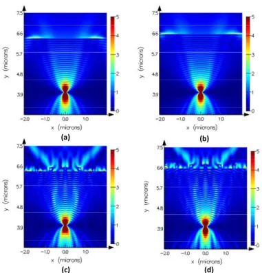
Figure 6 shows the simulated 2D intensity pattern of light exiting from LED in four different cases: (a) C-LED, (b) C-LED with ZnO wetting layer, (c) C-LED with ZnO nanorods and (d) C-LED with ZnO nanorod array on top of wetting layer. As shown by Fig. 6(a), most of the light that is generated in the active region of the LED, suffers the total internal reflection and is trapped within the LED structure. With the help of 200 nm thick ZnO wetting layer more amount of light can escape out the LED structure since ZnO wetting layer allows increase in the critical angle at air-ZnO boundary. In Fig. 6(c), light emission from the LED structure is studied with only ZnO nanorods. In this case, no ZnO wetting layer is present which helps to out-couple more light from the LED structure as shown in Fig. 6(b). However, with only ZnO nanorods present on the top of GaN LED surface, LEE of 1.7 times can be achieved due to multiple scattering from the side walls within ZnO nanostructure and emission from top surface [16,17]. In the last case, light scattered from ZnO nanorod array on the top of the ZnO wetting layer is shown by Fig. 6(d). In this case, both wetting layer and nanorod array assist in to escape more light from the GaN LED that is trapped inside achieving the LEE of 1.9. Thus, the ZnO wetting layer out-couples more light into the air whereas, ZnO nanorods allows light enhancement due to multiple scattering from the sidewalls and top surface.
(a) (b)
(d) (c)
Fig. 6. 2D light intensity pattern from numerical FDTD simulation in case of (a) C-LED, (b) C-LED with ZnO wetting layer, (c) C-LED with ZnO nanorod array and (d) C-LED with ZnO nanorod array on top of ZnO wetting layer.
4. Conclusion
In summary, large-scale ordered ZnO nanorods have been integrated on the GaN LED by a simple, cost-effective and efficient nanoimprinting method. The introduction of the imprinted ZnO nanorods does not degrade the electrical properties of the final LEDs thanks to the room-temperature processing, unlike the previous reports. As a result of light scattering effect combined with the enhancement of light extraction through the ZnO nanorod sidewalls, the LEE of the integrated ZnO-nanorod/GaN LED is remarkably improved. In comparison with the conventional LED, a 100% improvement in the light emission efficiency has been observed. This integration method holds great promise for improving the light extraction of LEDs to achieve the high-power LEDs.
Acknowledgments
This work is supported by the National Research Foundation of Singapore under Grant No. NRF-CRP-6-2010-2 and NRF-RF-2009-09 and the Singapore Agency for Science, Technology and Research (A*STAR) SERC under Grant No. 112 120 2009.