High bandwidth-efficiency resonant cavity enhanced Schottky photodiodes for 800–850
nm wavelength operation
M. S. Ünlü, M. Gökkavas, B. M. Onat, E. Ata, E. Özbay, R. P. Mirin, K. J. Knopp, K. A. Bertness, and D. H. Christensen
Citation: Appl. Phys. Lett. 72, 2727 (1998); doi: 10.1063/1.121073 View online: http://dx.doi.org/10.1063/1.121073
View Table of Contents: http://aip.scitation.org/toc/apl/72/21
Published by the American Institute of Physics
Articles you may be interested in
Resonant cavity enhanced photonic devices
High bandwidth-efficiency resonant cavity enhanced Schottky photodiodes
for 800–850 nm wavelength operation
M. S. U¨ nlu¨,a)M. Go¨kkavas, and B. M. Onat
Boston University, Department of Electrical and Computer Engineering, Photonics Center, Boston, Massachusetts 02215
E. Ata and E. O¨ zbay
Bilkent University, Physics Department, Ankara 06533, Turkey
R. P. Mirin, K. J. Knopp, K. A. Bertness, and D. H. Christensen National Institute of Standards and Technology, Boulder, Colorado 80303
~Received 10 March 1998; accepted for publication 24 March 1998!
High-speed resonant cavity enhanced Schottky photodiodes operating in 800–850 nm wavelength region are demonstrated. The devices are fabricated in the AlGaAs/GaAs material system. The Schottky contact is a semitransparent Au film which also serves as the top reflector of the Fabry– Perot cavity. The detectors exhibit a peak quantum efficiency ofh50.5 at l5827 nm wavelength and a 3 dB bandwidth of more than 50 GHz resulting in a bandwidth-efficiency product of more than 25 GHz. © 1998 American Institute of Physics.@S0003-6951~98!03021-6#
Schottky photodiodes~PD! are very attractive for high-speed photodetection, because of their simple material struc-ture and fabrication process. The optimized strucstruc-ture of a conventional high-speed Schottky PD typically requires a thin absorption region. As a result, the quantum efficiency is low at wavelengths where the absorption coefficientaof the semiconductor material is small. Although high performance Schottky PDs with semitransparent metal contacts have been successfully fabricated,1 the bandwidth-efficiency product has remained limited by the material properties. With the advent of GaAs vertical-cavity surface-emitting lasers
~VCSEL!,2 the 800–850 nm wavelength range has recently
emerged as a strong candidate for short distance optical com-munications. At these wavelengths, the quantum efficiency of high-speed GaAs Schottky PDs suffer from relatively small absorption coefficient. Resonant cavity enhanced
~RCE!3 photodetection scheme offers a new way of
increas-ing the quantum efficiency of detectors with thin absorbers. Various high-speed RCE photodetector structures have been demonstrated3with high bandwidth efficiency products espe-cially in avalanche photodiodes.4The RCE detection is par-ticularly attractive for Schottky-type photodetectors, since the semitransparent metal contact can also function as the top reflector.5 Recently, we have demonstrated very high-speed RCE Schottky PDs operating at 900 nm wavelength.6,7 At this wavelength, a thin pseudomorphic InGaAs layer serves as the absorption region in a cavity formed by a GaAs/AlAs distributed Bragg reflector~DBR! and GaAs contact regions. While the formation of the resonant cavity is relatively easy with the binary compound semiconductors~AlAs and GaAs! in the DBR, the operation wavelength is limited to 860–900 nm. In this article, we present experimental results on RCE Schottky PDs operating at 830 nm wavelength utilizing AlGaAs/AlAs DBR mirrors and GaAs absorption regions. Since the top reflector of the RCE structure is the Schottky
metal, the resonant wavelength can be adjusted3,8throughout the 800–850 nm range during device fabrication and can be used in optical communication systems utilizing 850 nm VC-SELs.
The device structure ~shown in Fig. 1! is designed to achieve a low-loss Fabry–Perot cavity for a spectral region of at least 50 nm wide centered around 830 nm wavelength. The layers are grown by molecular beam epitaxy on a semi-insulating GaAs substrate. The resonant cavity is formed by
a!Electronic mail: [email protected] FIG. 1. Schematic representation of the layer structure of the RCE SchottkyPDs. The band gap, E g, variation in the depletion region is also shown.
APPLIED PHYSICS LETTERS VOLUME 72, NUMBER 21 25 MAY 1998
2727
an Al0.2Ga0.8As/AlAs DBR bottom reflector and the
semi-transparent Au contact on top. Since the index contrast be-tween AlAs and Al0.2Ga0.8As is relatively small, a 19 period
mirror is grown to form a high-reflectivity bottom mirror. The wafers are characterized by reflectance measurements after the growth is completed. The experimentally observed resonance peak shifted to shorter wavelengths by approxi-mately 3 nm compared to computer simulations, indicating better than 0.5% accuracy in the growth of the structure. A 400 nm thick n1-AlGaAs layer grown on top of the bottom mirror is used for the Ohmic contact. The mole fraction of Al in the DBR and the contact regions is chosen as 0.2 to ensure a low-loss cavity throughout the entire operating spectrum. The normally depleted region of the Schottky PD consists of a combination of lightly doped GaAs and AlGaAs layers. At the operation wavelength, only the 120 nm thick GaAs re-gion absorbs the optical excitation. The Al mole fraction of the AlGaAs on top of the the thin GaAs absorption region is chosen as 0.15, slightly smaller than that of the bottom AlGaAs layers, to reduce the potential barrier for holes. Also, both AlGaAs/GaAs heterointerfaces are graded for 30 nm to eliminate abrupt potential barriers which may ad-versely affect the high-speed performance by trapping the photogenerated carriers. The position of the absorption layer in the depletion region is optimized to yield minimum transit time for electrons and holes. Standard photolithography, wet chemical etching, and mesa processes are utilized for device fabrication and the Schottky contact is formed by Au evapo-ration. To reduce the parasitic capacitance, the Schottky metal is connected to the contact pads by an Au airbridge. The electrical contacts are designed as 50V coplanar trans-mission lines for on-wafer high-speed characterization. On top of the Schottky metal, a dielectric layer (Si3N4) is used to optimize detector responsivity.
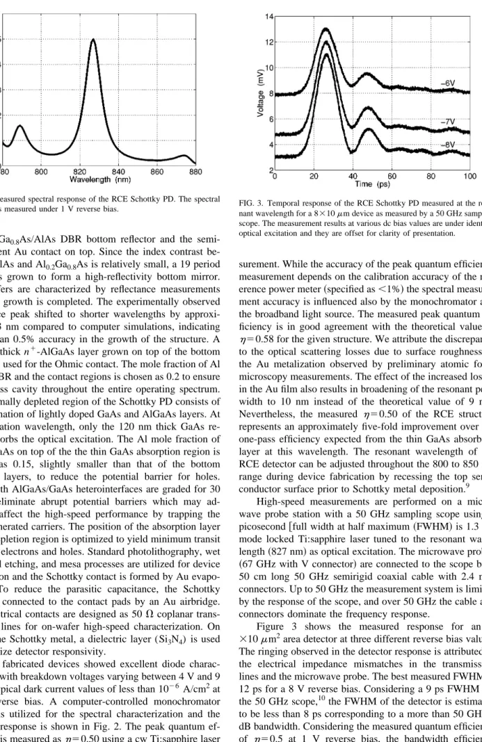
The fabricated devices showed excellent diode charac-teristics with breakdown voltages varying between 4 V and 9 V and typical dark current values of less than 1026 A/cm2at 1 V reverse bias. A computer-controlled monochromator system is utilized for the spectral characterization and the spectral response is shown in Fig. 2. The peak quantum ef-ficiency is measured ash50.50 using a cw Ti:sapphire laser tuned to the resonant wavelength~at 827 nm! for excitation and the spectral response is normalized based on this
mea-surement. While the accuracy of the peak quantum efficiency measurement depends on the calibration accuracy of the ref-erence power meter~specified as ,1%! the spectral measure-ment accuracy is influenced also by the monochromator and the broadband light source. The measured peak quantum ef-ficiency is in good agreement with the theoretical value of
h50.58 for the given structure. We attribute the discrepancy
to the optical scattering losses due to surface roughness of the Au metalization observed by preliminary atomic force microscopy measurements. The effect of the increased losses in the Au film also results in broadening of the resonant peak width to 10 nm instead of the theoretical value of 9 nm. Nevertheless, the measured h50.50 of the RCE structure represents an approximately five-fold improvement over the one-pass efficiency expected from the thin GaAs absorbing layer at this wavelength. The resonant wavelength of the RCE detector can be adjusted throughout the 800 to 850 nm range during device fabrication by recessing the top semi-conductor surface prior to Schottky metal deposition.9
High-speed measurements are performed on a micro-wave probe station with a 50 GHz sampling scope using a picosecond @full width at half maximum ~FWHM! is 1.3 ps# mode locked Ti:sapphire laser tuned to the resonant wave-length~827 nm! as optical excitation. The microwave probes
~67 GHz with V connector! are connected to the scope by a
50 cm long 50 GHz semirigid coaxial cable with 2.4 mm connectors. Up to 50 GHz the measurement system is limited by the response of the scope, and over 50 GHz the cable and connectors dominate the frequency response.
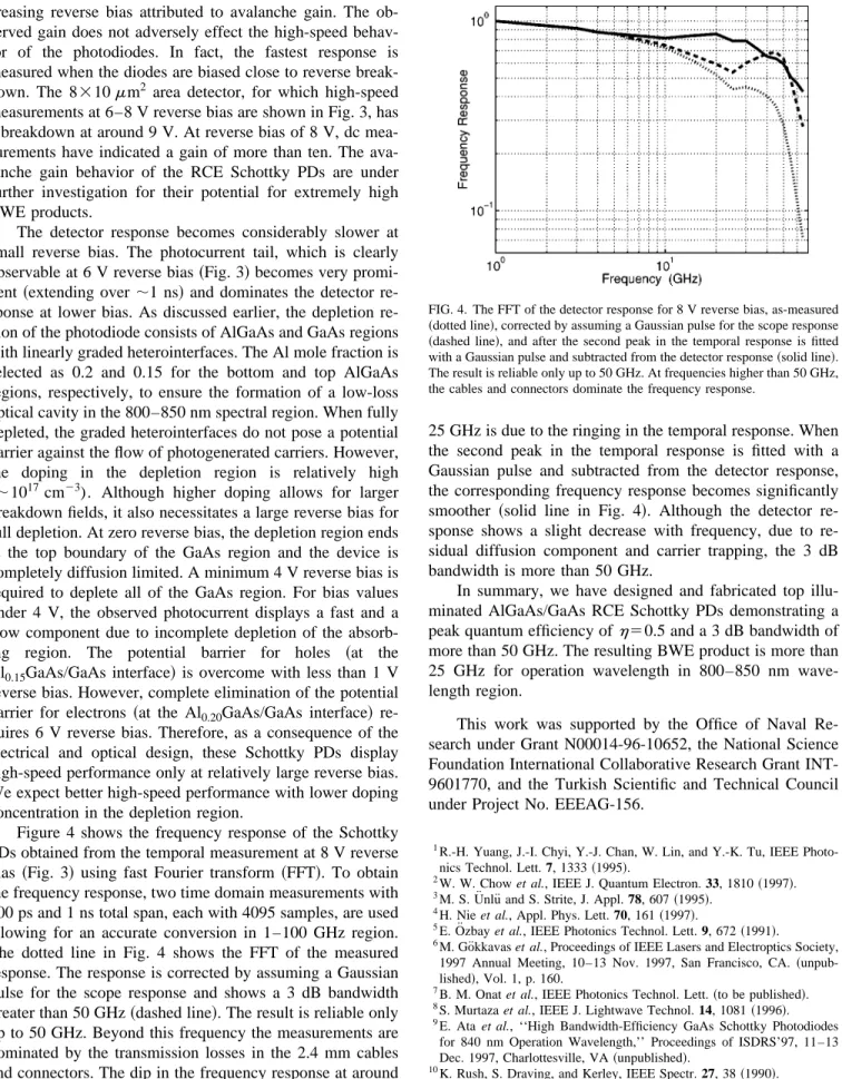
Figure 3 shows the measured response for an 8
310mm2area detector at three different reverse bias values. The ringing observed in the detector response is attributed to the electrical impedance mismatches in the transmission lines and the microwave probe. The best measured FWHM is 12 ps for a 8 V reverse bias. Considering a 9 ps FWHM for the 50 GHz scope,10the FWHM of the detector is estimated to be less than 8 ps corresponding to a more than 50 GHz 3 dB bandwidth. Considering the measured quantum efficiency of h50.5 at 1 V reverse bias, the bandwidth efficiency
~BWE! product is in excess of 25 GHz. We also observe an
increase in the responsivity of the photodetectors with
in-FIG. 2. Measured spectral response of the RCE Schottky PD. The spectral
response is measured under 1 V reverse bias. FIG. 3. Temporal response of the RCE Schottky PD measured at the reso-nant wavelength for a 8310mm device as measured by a 50 GHz sampling scope. The measurement results at various dc bias values are under identical optical excitation and they are offset for clarity of presentation.
creasing reverse bias attributed to avalanche gain. The ob-served gain does not adversely effect the high-speed behav-ior of the photodiodes. In fact, the fastest response is measured when the diodes are biased close to reverse break-down. The 8310mm2 area detector, for which high-speed measurements at 6–8 V reverse bias are shown in Fig. 3, has a breakdown at around 9 V. At reverse bias of 8 V, dc mea-surements have indicated a gain of more than ten. The ava-lanche gain behavior of the RCE Schottky PDs are under further investigation for their potential for extremely high BWE products.
The detector response becomes considerably slower at small reverse bias. The photocurrent tail, which is clearly observable at 6 V reverse bias~Fig. 3! becomes very promi-nent~extending over ;1 ns! and dominates the detector sponse at lower bias. As discussed earlier, the depletion re-gion of the photodiode consists of AlGaAs and GaAs rere-gions with linearly graded heterointerfaces. The Al mole fraction is selected as 0.2 and 0.15 for the bottom and top AlGaAs regions, respectively, to ensure the formation of a low-loss optical cavity in the 800–850 nm spectral region. When fully depleted, the graded heterointerfaces do not pose a potential barrier against the flow of photogenerated carriers. However, the doping in the depletion region is relatively high (;1017 cm23). Although higher doping allows for larger breakdown fields, it also necessitates a large reverse bias for full depletion. At zero reverse bias, the depletion region ends at the top boundary of the GaAs region and the device is completely diffusion limited. A minimum 4 V reverse bias is required to deplete all of the GaAs region. For bias values under 4 V, the observed photocurrent displays a fast and a slow component due to incomplete depletion of the absorb-ing region. The potential barrier for holes ~at the Al0.15GaAs/GaAs interface! is overcome with less than 1 V
reverse bias. However, complete elimination of the potential barrier for electrons ~at the Al0.20GaAs/GaAs interface!
re-quires 6 V reverse bias. Therefore, as a consequence of the electrical and optical design, these Schottky PDs display high-speed performance only at relatively large reverse bias. We expect better high-speed performance with lower doping concentration in the depletion region.
Figure 4 shows the frequency response of the Schottky PDs obtained from the temporal measurement at 8 V reverse bias ~Fig. 3! using fast Fourier transform ~FFT!. To obtain the frequency response, two time domain measurements with 200 ps and 1 ns total span, each with 4095 samples, are used allowing for an accurate conversion in 1–100 GHz region. The dotted line in Fig. 4 shows the FFT of the measured response. The response is corrected by assuming a Gaussian pulse for the scope response and shows a 3 dB bandwidth greater than 50 GHz~dashed line!. The result is reliable only up to 50 GHz. Beyond this frequency the measurements are dominated by the transmission losses in the 2.4 mm cables and connectors. The dip in the frequency response at around
25 GHz is due to the ringing in the temporal response. When the second peak in the temporal response is fitted with a Gaussian pulse and subtracted from the detector response, the corresponding frequency response becomes significantly smoother ~solid line in Fig. 4!. Although the detector sponse shows a slight decrease with frequency, due to re-sidual diffusion component and carrier trapping, the 3 dB bandwidth is more than 50 GHz.
In summary, we have designed and fabricated top illu-minated AlGaAs/GaAs RCE Schottky PDs demonstrating a peak quantum efficiency ofh50.5 and a 3 dB bandwidth of more than 50 GHz. The resulting BWE product is more than 25 GHz for operation wavelength in 800–850 nm wave-length region.
This work was supported by the Office of Naval Re-search under Grant N00014-96-10652, the National Science Foundation International Collaborative Research Grant INT-9601770, and the Turkish Scientific and Technical Council under Project No. EEEAG-156.
1
R.-H. Yuang, J.-I. Chyi, Y.-J. Chan, W. Lin, and Y.-K. Tu, IEEE Photo-nics Technol. Lett. 7, 1333~1995!.
2W. W. Chow et al., IEEE J. Quantum Electron. 33, 1810~1997!. 3M. S. U¨ nlu¨ and S. Strite, J. Appl. 78, 607 ~1995!.
4
H. Nie et al., Appl. Phys. Lett. 70, 161~1997!.
5
E. O¨ zbay et al., IEEE Photonics Technol. Lett. 9, 672 ~1991!.
6M. Go¨kkavas et al., Proceedings of IEEE Lasers and Electroptics Society,
1997 Annual Meeting, 10–13 Nov. 1997, San Francisco, CA. ~unpub-lished!, Vol. 1, p. 160.
7
B. M. Onat et al., IEEE Photonics Technol. Lett.~to be published!.
8S. Murtaza et al., IEEE J. Lightwave Technol. 14, 1081~1996!. 9E. Ata et al., ‘‘High Bandwidth-Efficiency GaAs Schottky Photodiodes
for 840 nm Operation Wavelength,’’ Proceedings of ISDRS’97, 11–13 Dec. 1997, Charlottesville, VA~unpublished!.
10
K. Rush, S. Draving, and Kerley, IEEE Spectr. 27, 38~1990!.
FIG. 4. The FFT of the detector response for 8 V reverse bias, as-measured ~dotted line!, corrected by assuming a Gaussian pulse for the scope response ~dashed line!, and after the second peak in the temporal response is fitted with a Gaussian pulse and subtracted from the detector response~solid line!. The result is reliable only up to 50 GHz. At frequencies higher than 50 GHz, the cables and connectors dominate the frequency response.
2729