Large zero-field spin splitting in AlGaN/AlN/GaN/AlN heterostructures
S. B. Lisesivdin, N. Balkan, O. Makarovsky, A. Patanè, A. Yildiz, M. D. Caliskan, M. Kasap, S. Ozcelik, and E. Ozbay
Citation: Journal of Applied Physics 105, 093701 (2009); View online: https://doi.org/10.1063/1.3120782
View Table of Contents: http://aip.scitation.org/toc/jap/105/9 Published by the American Institute of Physics
Articles you may be interested in
Zero-field spin splitting in heterostructures with various Al compositions Applied Physics Letters 93, 172113 (2008); 10.1063/1.3012361
Weak antilocalization and beating pattern in high electron mobility two-dimensional electron gas with strong Rashba spin-orbit coupling
Large zero-field spin splitting in AlGaN/AlN/GaN/AlN heterostructures
S. B. Lisesivdin,1,2,a兲 N. Balkan,1O. Makarovsky,3A. Patanè,3A. Yildiz,4M. D. Caliskan,5 M. Kasap,2S. Ozcelik,2and E. Ozbay5,6
1
Department of Computing and Electronic Systems, University of Essex, CO4 3SQ Colchester, United Kingdom
2Department of Physics, Gazi University, Teknikokullar, 06500 Ankara, Turkey
3School of Physics and Astronomy, University of Nottingham, NG7 2RD, United Kingdom
4Department of Physics, Faculty of Science and Arts, Ahi Evran University, Asikpasa Kampusu, 40040 Kirsehir, Turkey
5Nanotechnology Research Center, Bilkent University, Bilkent, 06800 Ankara, Turkey
6Department of Physics, Department of Electrical and Electronics Engineering, Bilkent University, Bilkent, 06800 Ankara, Turkey
共Received 30 October 2008; accepted 23 March 2009; published online 1 May 2009兲
This work describes Shubnikov–de Haas 共SdH兲 measurements in Al0.22Ga0.78N/AlN/GaN/AlN
heterostructures. Our experiments coupled with the analysis of the Hall data at various temperatures confirm the formation of a two-dimensional electron gas 共2DEG兲 at the AlN/GaN interface. A beating pattern in the SdH oscillations is also observed and attributed to a zero-field spin splitting of the 2DEG first energy subband. The values of the effective spin-orbit coupling parameter and zero-field spin-split energy are estimated and compared with those reported in the literature. We show that zero-field spin-split energy tends to increase with increasing sheet electron density and that our value 共12.75 meV兲 is the largest one reported in the literature for GaN-based heterostructures. © 2009 American Institute of Physics.关DOI:10.1063/1.3120782兴
I. INTRODUCTION
The electronic properties of two-dimensional electron gases 共2DEGs兲 in AlxGa1−xN/GaN, AlxGa1−xN/AlN/
GaN, and AlxGa1−xN/AlN/GaN/AlN heterostructures have
been studied extensively for applications in high-power, high-temperature microwave devices and high-frequency high electron mobility transistors 共HEMTs兲.1–4 Recent im-provements in transport parameters, such as mobility and sheet electron density, have also led to increased interest in studies of the quantum Hall effect.5,6Due to the existence of high electrical fields caused by piezoelectric and spontaneous polarization, GaN-based heterostructures have an intrinsic 2DEG with high sheet carrier densities.7,8 These electric fields also enhance the spin-orbit interaction thus leading to a finite spin energy splitting of the conduction band states even in the absence of externally applied magnetic fields.9,10Zero spin splitting plays a key role in the high Curie temperatures and ferromagnetic properties reported in previous studies of wide bandgap semiconductors, such as GaN and ZnO.11,12 Therefore GaN-based heterostructures are also promising candidates for applications in spintronics.
Spin-orbit interaction and spin splitting in zincblende III–V materials have been studied extensively and are under-stood to a high degree.13Unlike the zincblende structures, in wurtzite low dimensional structures, there is an extra spin splitting term due to the lack of inversion symmetry in the wurtzite-type lattice.12 Recent experimental work indicate a serious disagreement between the results obtained from Shubnikov–de Haas 共SdH兲14–18 and weak antilocalization
共WAL兲,10,17,19–22
measurements. Also, circular photogalvanic23measurements suggest that spin-splitting en-ergy values should lie in the range from 0.1 to 9 meV.18,21 The reason for the disagreement and conflicting results is yet to be established.
The theoretical estimation for the Rashba dominated spin-splitting energy is, however, only ⬃1 meV.24 Lo et
al.25proposed an additional spin-splitting mechanism called ⌬C1−⌬C3 coupling, where the band folding generates two
conduction bands for the wurtzite structures and the coupling between these conduction bands enhances the spin-splitting energy. Therefore, Lo et al. concluded that the band folding and lack of inversion symmetry significantly contribute to the spin splitting in wurtzite GaN-based quantum wells.25
In this work, we report a detailed study of SdH oscilla-tions in an AlGaN/AlN/GaN/AlN heterostructure with high Hall mobility and sheet carrier density. Our experiment and analysis allow us to estimate the effective spin-orbit coupling parameter and zero-field spin-split energy, E↑− E↓. To our knowledge, our value of E↑− E↓⬃13 meV is the largest value reported in the literature for GaN-based heterostruc-tures. This result is relevant for future developments of GaN-based spintronic devices, such as spin-polarized field effect transistors.
II. EXPERIMENTAL TECHNIQUES
The samples used in the present study were all grown on
c-plane 共0001兲 sapphire 共Al2O3兲 substrate by low-pressure
Metal-Organic Chemical Vapor Deposition 共MOCVD兲. Hy-drogen was used as the carrier gas and trimethylgallium, tri-methylaluminum, and ammonia were used as Ga, Al, and N precursors, respectively. The substrate was cleaned in H2 am-a兲Author to whom correspondence should be addressed. Electronic mail:
bient at 1100 ° C and then a 15 nm low-temperature 共LT兲 AlN nucleation layer was grown at 840 ° C with 50 mbar reactor pressure. After the deposition of the LT-AlN nucle-ation layer, the wafers were heated to a high temperature 共HT兲 for annealing. For all samples, a HT-AlN buffer layer of thickness of about 0.60 m was deposited on the an-nealed nucleation layers at 1127 ° C with a 400 nm/h growth rate. After the deposition of the buffer layer, a HT-GaN layer with an approximate thickness of 1.9 m was grown at 1040 ° C. Finally, a 1.5 nm thick AlN interlayer, a 27 nm thick Al0.22Ga0.78N barrier layer, and a 3 nm GaN cap layer
were grown at 1080 ° C. All layers were nominally undoped. Details of the sample layer structure are shown in Fig.1.
For the resistivity and Hall measurements by the Van der Pauw method, square shaped共5⫻5 mm2兲 samples were
pre-pared with four evaporated and annealed Ti/Al/Ni/Au 共200 Å/2000 Å/300 Å/700 Å兲 Ohmic contacts in the corners. Gold wires were soldered to the contacts with indium. The Ohmic behavior of the contacts was confirmed by the form of the current voltage characteristics, which are symmetrical with respect to the polarity of the applied voltage. Hall measure-ments were carried out in the temperature range of 2–350 K. The Hall coefficient and resistivity were measured for both directions of current, magnetic field polarizations, and for all possible contact configurations.
III. RESULTS AND DISCUSSION
Figure2 shows the temperature dependence of the Hall mobility and Hall sheet carrier density for the samples inves-tigated in the current study. LT共2 K兲 Hall mobility and Hall sheet carrier density are 19 950 cm2/V s and 1.05
⫻1013 cm−2, respectively. As shown in Fig.2, the Hall
mo-bility is nearly temperature independent below 100 K, but decreases with increasing temperature above 100 K, as ex-pected from an increasing dominance of polar optical pho-non scattering. In addition, the sheet carrier density is nearly independent of temperature in the whole range of tempera-tures, except at HTs where it tends to increase slightly due to
thermal activation of bulk carriers. The behavior of both mo-bility and sheet carrier density is typical of 2DEGs.
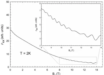
Figure3 shows a typical longitudinal magnetoresistivity measurement关xx共Bz兲兴 as a function of a perpendicular
mag-netic field, Bz, at 2 K. The SdH oscillations at magnetic fields
between 8 and 14 T are shown in the insert of Fig. 3. The negative parabolic magnetoresistance in this magnetic field range was also observed by Brana et al.26 and attributed to diffusive electron-electron interactions. In order to extract the contribution of the parabolic background magnetoresis-tance from the SdH oscillations, we used a general method and calculated the negative second derivative 共−2R
xx/B2兲
of the raw magnetic field dependent experimental data with respect to magnetic field and plotted the results as a function of inverse magnetic field in Fig. 4.27–30The beating pattern superimposed on the periodic SdH oscillations is clearly seen in this figure. In order to obtain the characteristic frequencies of these oscillations, we used fast Fourier transform 共FFT兲 analysis. The results of the FFT analysis are shown in the insert of Fig. 4. We obtain two distinct SdH frequencies f1
= 202.7 and f2= 226.1 T.
For structures similar to ours, Lo et al.15proposed three possible mechanisms for the beating effect:共i兲 spin splitting of the 2DEG first energy subband,共ii兲 two-subbands occupa-FIG. 1. Layer structure of our samples.
FIG. 2. Temperature dependent Hall mobility and Hall sheet carrier density of our samples. Lines are guides to the eyes.
FIG. 3. Magnetic field dependent longitudinal magnetoresistivity关xx共Bz兲兴 at 2 K. Insert: SdH oscillations in the range of magnetic fields 8–14 T.
tion, and共iii兲 second 2D channel located in the barrier layer. A fourth possible mechanism is the existence of a two-dimensional hole gas 共2DHG兲 between the GaN and AlN buffer layers.31 In order to establish the existence of this 2DHG, magnetic field dependent Hall measurements were carried out and the results were analyzed using the quantita-tive mobility spectrum analysis共QMSA兲 technique reported by us in our previous studies on similar GaN-based heterostructures.32–34 Mobility spectra at temperatures T = 22 K and T = 159 K are shown in Figs. 5共a兲and5共b兲, re-spectively. It is clear from the figure that the 2DEG conduc-tion is dominant and there is a negligible contribuconduc-tion from the hole channel. Therefore we infer that Hall mobility and Hall sheet carrier density shown in Fig.2are due only to the 2DEG at the AlN/GaN heterojunction. The existence of a 2D channel in the barrier layer is also dismissed through a lack of evidence in the QMSA analysis. The second potential source for the observed beating is the double subband occu-pancy, which we exclude for the following reasons. Using the well known relation
⌬i
冉
1 B冊
= e បni , 共1兲we calculated the electron density for the two subbands by using the SdH frequencies shown in the insert of Fig. 4.35 Here, niis the carrier density of the ith subband and⌬iis the
period in 1/B of the SdH oscillations. Using Eq.共1兲, we find that the carrier densities of the first two energy subbands are
n1= 1.09⫻1013 and n2= 9.77⫻1012 cm−2. The total carrier
density is n1+ n2⬵2.07⫻1013 cm−2and is much larger than
the Hall sheet carrier density of 1.05⫻1013 cm−2 shown in
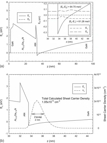
Fig.2. Therefore, the beating effect cannot be related to the two-subband occupancy. In order to further justify this ob-servation, we solved self-consistently the nonlinear Schrödinger–Poisson equations for our Al0.22Ga0.78N/ AlN/GaN/AlN HEMT structure.36
The results are shown in Fig.6. The subband energies and related electron wave func-tions are shown in the insert of Fig. 6共a兲 for T = 2 K. As shown in Fig.6共a兲, the Fermi level is 64.70 meV below the second subband. The first subband is 61.28 meV below the Fermi level and is occupied at 2 K. The energy separation between the two subbands is E2− E1= 125.98 meV. This
value is similar to both theoretical and experimental results reported for the AlGaN/GaN structures by several groups.15,37The carrier population at the AlN/GaN interface is shown in Fig. 6共b兲. Here, the sheet carrier density values FIG. 4. The negative second derivative of the magnetoresistance关Rxx共Bz兲兴
with respect to an inverse magnetic field. The insert shows two main fre-quencies derived from the Fourier analysis of the the SdH oscillations.
FIG. 5. Electron共solid lines兲 and hole 共dashed lines兲 QMSA spectra at 共a兲 22 and共b兲 159 K.
(b) (a)
FIG. 6.共a兲 Conduction band profile 共full line兲 and Fermi level 共dashed line兲 for our Al0.22Ga0.78N/AlN/GaN/AlN heterostructure. Insert: first two sub-band energies and Fermi level and related electron wave functions.共b兲 Con-duction band profile共full line兲 and calculated sheet carrier density 共dashed line兲.
are calculated assuming a 2DEG thickness of 2 nm. As seen in Figs.6共a兲,6共b兲, and2, the calculated sheet carrier density is in perfect agreement with the Hall measurements. There-fore we conclude that only a single subband is populated and that the origin of the beating effect is the spin splitting of the first energy subband.
To describe zero-field spin splitting, an effective mag-netic field can be defined so that the spin Hamiltonian will be
H =1
2ប· Beff共k储兲, 共2兲
where is the Pauli matrices vector and the k储 is the
in-plane wave vector.38 Magnitude and the direction of the ef-fective magnetic field are depending on in-plane wave vector as seen on Eq.共2兲. For the single subband case, the in-plane wave vector dependent spin-splitting can be given by38
⌬共k储兲ប兩Beff兩. 共3兲
A spin-orbit Hamiltonian was proposed by Bychkov and Rashba to represent spin-orbit interactions as H =␣共 ⫻k兲·zˆ.39
Here,␣is the structure dependent parameter; spin-orbit coupling constant and zˆ is the unit vector along the growth direction. So the effective magnetic field can be found as
Bso=共2/ប兲␣k⫻ zˆ. 共4兲
Effective magnetic field written in Eq.共4兲 concludes a spin-splitting value of ⌬=2␣k储. Zero-field spin splitting
gives rise to a similar beating pattern to that related to the magnetointersubband scattering共MIS兲 effect and, therefore, the exact calculation of the subband positions is also impor-tant for the investigation of the spin related beating pattern.40 The MIS effect occurs when a second subband is populated.41 In AlGaN/GaN with a high Al composition or AlGaN/AlN/GaN structures, MIS becomes increasingly im-portant compared to the zero-field spin splitting at elevated temperatures and when the intersubband energy separation is small.18 According to our calculations shown in Figs. 6共a兲
and6共b兲, our samples have single subband occupancy with a high carrier density, in which the beating of the SdH oscilla-tions is related to the zero-field spin splitting. The relation between the SdH frequencies and the carrier densities of spin-up共spin-down兲 electrons is18
f↑共↓兲=hn↑共↓兲
e , 共5兲
where f↑共↓兲 is the SdH frequency for spin-up 共spin-down兲 electrons and its value is measured from the insert of Fig.4
as 202.7 T and 226.1 T for spin-up and spin down electrons, respectively. Using Eq. 共5兲, the carrier densities of spin-up and spin-down electrons are calculated as n↑= 5.46⫻1012 and n↓= 4.90⫻1012 cm−2. The total carrier density共n↑+ n↓兲 is consistent with the Hall sheet carrier density of 1.05 ⫻1013 cm−2within an experimental accuracy of about 3%.
Once the carrier densities of spin-up and spin-down elec-trons are known, the spin-orbit coupling parameter␣ can be found using the relation42
␣=⌬nប 2 mⴱ
冑
2共ns−⌬n兲 . 共6兲Here,⌬n is the difference in carrier densities of spin-up and spin-down electrons ⌬n=5.6⫻1011 cm−2 and n
s= n↑
+ n↓. From Eq.共6兲, we obtain the spin-orbit coupling param-eter,␣= 7.85⫻10−12 eV m. While this value is much larger
than that found in other heterostructure systems such as InAs/GaSb, InxGa1−xAs/In0.52Al0.48As, In0.53Ga0.47As/
In0.77Ga0.23As/InP,42–44 it agrees with the values of ␣ for
AlGaN/GaN heterostructures.15,38 In III-N structures, the higher value of the spin-orbit coupling parameter is likely to be caused by the strong internal electric fields induced by piezoelectric and spontaneous polarization.8,45The calculated spin-orbit coupling parameter is a sum of the Rashba param-eter ␣R and a coupling parameter associated with the bulk
inversion asymmetry in wurtzite quantum wells ␣WBIA.12
Zero-field spin splitting energy共⌬兲 can be calculated, there-fore, from effective spin-orbit coupling parameter. The cal-culated value of 2␣k is 12.75 meV. This is in good agreement
with the spin-split energy of 12.30 meV obtained from the SdH frequencies as
E↑− E↓=2ប
2⌬n
mⴱ . 共7兲
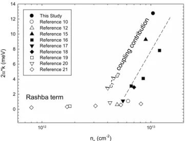
The list of the growth and electrical parameters are listed together with the spin related parameters and experimental methods used in the evaluation of the spin-splitting energy in AlGaN/GaN and AlGaN/AlN/GaN obtained by us and others10,12,15–21is given in TableI.
Figure7shows the zero-field spin splitting energy versus sheet carrier density data from Table I. The WAL measure-ment results are shown with empty symbols and SdH mea-surements are shown with filled symbols. It is clear that there is a significant disagreement between WAL and SdH results. The WAL measurements show good agreement with the the-oretical estimate based on the Rashba coupling mechanism.24 It should be noted that the SdH measurements fail in samples with sheet carrier densities below nS⬃6⫻10−12 cm−2 as a
result of the lack of beating patterns. However, at sheet car-rier densities above 6⫻10−12 cm−2, the spin-splitting energy values begin from Rashba value and increase with the in-creasing sheet carrier density. This increase could be caused by the⌬C1−⌬C3coupling, where the band folding generates two conduction bands, and by the lack of an inversion sym-metry effect.25 An increase in the zero-field spin splitting with the increasing sheet carrier density is also expected ac-cording to the theoretical work by Litvinov.24 However, the reason for the disagreement between the SdH and WAL mea-surements is not clear to us.
IV. CONCLUSION
We studied the magnetoresistivity of a 2DEG in AlGaN/ AlN/GaN/AlN heterostructures at low temperatures 共T = 2 K兲 and high magnetic fields 共up to 14 T兲. We confirmed that the 2DEG has high mobility and high sheet carrier den-sity and that the effect of any parallel conduction channel is negligible. We observed a beating effect in the SdH
tions, which was attributed to zero-field spin splitting. This conclusion was supported with a one-dimensional self-consistent nonlinear Schrödinger–Poisson equation solution and analytic calculations of spin carrier density. For the zero-field spin splitting mechanism, an effective spin-orbit cou-pling parameter along with zero-field spin splitting energy values were calculated and compared with the literature. To
our knowledge, the zero-field spin splitting energy observed in our structure共12.75 meV兲 is the largest value reported so far in the literature for the GaN-based systems. Comparison with the recent literature indicates disagreement between the values obtained using WAL and SdH experiments. SdH mea-surements cannot be used for sheet carrier densities under 6⫻10−12 cm−2 due to lack of beating patterns where the WAL measurements show good agreement with the theoret-ical values based on the Rashba coupling mechanism.24 In SdH experiments at sheet carrier densities above 6 ⫻10−12 cm−2, the spin-splitting energy values begin from
Rashba value and increase with the increasing sheet carrier density. This increase could be caused by the⌬C1−⌬C3 cou-pling. It is also predicted by the theoretical work by Litvinov.24
ACKNOWLEDGMENTS
This work is supported by the State of Planning Organi-zation of Turkey under Grant No. 2001K120590 and by TU-BITAK under Project Nos. 104E090, 105E066, and 105A005. S. B. Lisesivdin acknowledges a 2214 coded in-ternational research scholarship from TUBITAK 共Turkey兲, A.P. acknowledges support from the Engineering and Physi-cal Sciences Research Council共UK兲 and E.O. acknowledges partial support from the Turkish Academy of Sciences 共Tur-key兲.
1M. Asif Khan, J. N. Kuznia, J. M. Van Hove, N. Pan, and J. Carter,Appl.
TABLE I. Growth, electrical and spin related parameters, and experimental method used to calculate the spin-splitting energy for our AlGaN/AlN/GaN/AlN samples and for AlGaN/GaN and AlGaN/AlN/GaN structures in the literature共Refs.10,12, and15–21兲.
Sample T 共K兲 x共Al兲 d共AlGaN兲 共nm兲 d共AlN兲 共nm兲 ns 共1⫻1012 cm−2兲 Experimental method ␣ⴱ 共1⫻10−12 eV m兲 2␣ⴱk 共meV兲a
Single sample typeb 0.1 0.3 20 0 6.20 WAL 0.85 1.06
Sample Cc 1.6 0.15 25 1 4.90 WAL 0.55 0.61
Sample 3d 1.2 0.25 30e 0 8.96 SdH 6.18 9.27
Sample Af 2 0.11 30 0 6.6 SdH 2.4 3.09
Sample Bf 2 0.25 28 0 8.5 SdH 2.8 4.09
Sample Cf 2 0.28 25 0 12 SdH 4.5 7.81
Single sample typeg 1.5 0.11 23 0 5.5 SdH 0.94 1.11
Single sample typeh 2 0.11 30 0 7.00 SdH 2.20 2.92
Sample Bi 0.3 0.12 16 0 1.8 WAL 0.6 0.40 Sample 1j 1 0.15 35 0 4.21 WAL 0.85 0.87 Sample Ak 1.8 0.1 25 1 0.8 WAL 5.0 0.22 Sample Bk 1.8 0.15 25 1 1.7 WAL 5.0 0.33 Sample Ck 1.8 0.25 25 1 3.1 WAL 5.0 0.44 Sample Dk 1.8 0.3 25 1 5.3 WAL 5.0 0.58 Sample Ek 1.8 0.35 25 1 8.1 WAL 5.0 0.71 This study 2 0.22 25 1.5 10.50 SdH 7.85 12.75
aCalculated using Hall carrier densities for the wave vector. bReference10.
cReference12. dReference15.
e20 nm n-type with 1.7⫻1017 cm−3Si doping +10 nm undoped. fReference16. gReference17. hReference18. iReference19. jReference20. kReference21.
FIG. 7. Sheet carrier density dependent zero-field spin splitting energy val-ues using data listed in TableI. Filled and empty symbols represent SdH and WAL experiment results, respectively. Dashed line is guide to the eyes and dotted line represents the theoretical value based on the Rashba coupling mechanism.
Phys. Lett.60, 3027共1992兲.
2Z. Fan, C. Lu, A. E. Botchkarev, H. Tang, A. Salvador, O. Aktas, W. Kim,
and H. Morkoc,Electron. Lett.33, 814共1997兲.
3U. K. Mishra, Y.-F. Wu, B. P. Keller, S. Keller, and S. P. DenBaars,IEEE Trans. Microwave Theory Tech.46, 756共1998兲.
4N. Maeda, T. Saitoh, K. Tsubaki, T. Nishida, and N. Kobayashi,Jpn. J. Appl. Phys., Part 238, L799共1999兲.
5W. Knap, H. Alause, J. M. Bluet, J. Camassel, J. Young, M. Asif Khan, Q.
Chen, S. Huant, and M. Shur,Solid State Commun.99, 195共1996兲. 6W. Knap, S. Contreras, H. Alause, C. Skierbiszewski, J. Camassel, M.
Dyakonov, J. L. Robert, J. Yang, Q. Chen, M. Asif Khan, M. L. Sadowski, and S. Huant,Appl. Phys. Lett.70, 2123共1997兲.
7O. Ambacher, B. Foutz, J. Smart, J. R. Shealy, N. G. Weimann, K. Chu,
M. Murphy, A. J. Sierakowski, W. J. Schaff, L. F. Eastman, R. Dimitrov, A. Mitchell, and M. Stutzmann,J. Appl. Phys.87, 334共2000兲.
8F. Bernardini, V. Fiorentini, and D. Vanderbilt,Phys. Rev. B56, R10024
共1997兲.
9I. Zutic, J. Fabian, and S. Das Sarma,Rev. Mod. Phys.76, 323共2004兲. 10N. Thillosen, Th. Schäpers, N. Kaluza, H. Hardtdegen, and V. A.
Guzenko,Appl. Phys. Lett.88, 022111共2006兲.
11S. A. Wolf, D. D. Awschalom, R. A. Buhrman, J. M. Daughton, S. von
Molnár, M. L. Roukes, A. Y. Chtchelkanova, and D. M. Treger,Science 294, 1488共2001兲.
12C. Kurdak, N. Biyikli, U. Ozgur, H. Morkoc, and V. I. Litvinov,Phys. Rev. B74, 113308共2006兲.
13P. D. Dresselhaus, C. M. A. Papavassiliou, R. G. Wheeler, and R. N.
Sacks,Phys. Rev. Lett.68, 106共1992兲.
14K. Tsubaki, N. Maeda, T. Saitoh, and N. Kobayashi,Appl. Phys. Lett.80,
3126共2002兲.
15I. Lo, J. K. Tsai, W. J. Yao, P. C. Ho, L.–W. Tu, T. C. Chang, S. Elhamri,
W. C. Mitchel, K. Y. Hsieh, J. H. Huang, H. L. Huang, and W.–C. Tsai,
Phys. Rev. B65, 161306共2002兲.
16N. Tang, B. Shen, K. Han, F.-C. Lu, F.-J. Xu, Z.-X. Qin, and G.-Y. Zhang, Appl. Phys. Lett.93, 172113共2008兲.
17W. Z. Zhou, T. Lin, L. Y. Shang, L. Sun, K. H. Gao, Y. M. Zhou, G. Yu,
N. Tang, K. Han, B. Shen, S. L. Guo, Y. S. Gui, and J. H. Chu,J. Appl. Phys.104, 053703共2008兲.
18N. Tang, B. Shen, M. J. Wang, K. Han, Z. J. Yang, K. Xu, G. Y. Zhang, T.
Lin, B. Zhu, W. Z. Zhou, and J. H. Chu,Appl. Phys. Lett.88, 172112
共2006兲.
19S. Schmult, M. J. Manfra, A. Punnoose, A. M. Sergent, K. W. Baldwin,
and R. J. Molnar,Phys. Rev. B74, 033302共2006兲.
20N. Thillosen, S. Cabanas, N. Kaluza, V. A. Guzenko, H. Hardtdegen, and
Th. Schäpers,Phys. Rev. B75, 241311共R兲 共2006兲.
21H. Cheng, N. Biyikli, U. Ozgur, C. Kurdak, H. Morkoc, and V. I. Litvinov, Physica E40, 1586共2008兲.
22E. B. Olshanetsky, Z. D. Kvon, S. Sassine, J. C. Portal, H. I. Cho, and J.
H. Lee,Appl. Phys. Lett.92, 242112共2008兲.
23W. Weber, S. D. Ganichev, S. N. Danilov, D. Weiss, W. Prettl, Z. D. Kvon,
V. V. Belkov, L. E. Golub, H.-I. Cho, and J.-H. Lee,Appl. Phys. Lett.87,
262106共2005兲.
24V. I. Litvinov,Phys. Rev. B68, 155314共2003兲.
25I. Lo, W. T. Wang, M. H. Gau, S. F. Tsay, and J. C. Chiang,Phys. Rev. B 72, 245329共2005兲.
26A. F. Brana, C. Diaz–Paniagua, F. Batallan, J. A. Garrido, E. Munoz, and
F. Omnes,J. Appl. Phys.88, 932共2000兲.
27D. G. Seiler and A. E. Stephens, in Landau Level Spectroscopy, edited by
G. Landwehr and E. I. Rashba共North-Holland, Amsterdam, 1991兲, Vol. 2, p. 1031.
28D. R. Leadley, R. J. Nicholas, J. J. Harris, and C. T. Foxon,Semicond. Sci. Technol.4, 885共1989兲.
29H. Celik, M. Cankurtaran, A. Bayrakli, E. Tiras, and N. Balkan, Semi-cond. Sci. Technol.12, 389共1997兲.
30E. Tiras, M. Cankurtaran, H. Celik, A. B. Thoms, and N. Balkan, Super-lattices Microstruct.29, 147共2001兲.
31S. Acar, S. B. Lisesivdin, M. Kasap, S. Ozcelik, and E. Ozbay,Thin Solid Films516, 2041共2008兲.
32S. B. Lisesivdin, A. Yildiz, S. Acar, M. Kasap, S. Ozcelik, and E. Ozbay, Appl. Phys. Lett.91, 102113共2007兲.
33S. B. Lisesivdin, S. Acar, M. Kasap, S. Ozcelik, S. Gokden, and E. Ozbay, Semicond. Sci. Technol.22, 543共2007兲.
34S. B. Lisesivdin, A. Yildiz, S. Acar, M. Kasap, S. Ozcelik, and E. Ozbay, Physica B399, 132共2007兲.
35I. Lo, W. C. Mitchel, M. Ahoujja, J.-P. Cheng, A. Fathimulla, and H. Mier, Appl. Phys. Lett.66, 754共1995兲.
36S. Birner, S. Hackenbuchner, M. Sabathil, G. Zandler, J. A. Majewski, T.
Andlauer, T. Zibold, R. Morschl, A. Trellakis, and P. Vogl, Acta Phys. Pol. A 110, 111共2006兲.
37J. A. Garrido, J. L. Sanchez–Rojas, A. Jimenez, E. Munoz, F. Omnes, and
P. Gibart,Appl. Phys. Lett.75, 2407共1999兲.
38E. A. de Andrada e Silva,Phys. Rev. B46, 1921共1992兲. 39Y. A. Bychkov and E. I. Rashba,J. Phys. C17, 6039共1984兲.
40N. Tang, B. Shen, Z. W. Zheng, J. Liu, D. J. Chen, J. Lu, R. Zhang, Y. Shi,
Y. D. Zheng, Y. S. Gui, C. P. Jiang, Z. J. Qiu, S. L. Guo, J. H. Chu, K. Hoshino, T. Someya, and Y. Arakawa,J. Appl. Phys.94, 5420共2003兲. 41T. H. Sander, S. N. Holmes, J. J. Harris, D. K. Maude, and J. C. Portal,
Phys. Rev. B58, 13856共1998兲.
42Th. Schäpers, G. Engels, J. Lange, T. Klocke, M. Hollfelder, and H. Lüth, J. Appl. Phys.83, 4324共1998兲.
43J. Luo, H. Munekata, F. F. Fang, and P. J. Stiles,Phys. Rev. B41, 7685
共1990兲.
44B. Das, S. Datta, and R. Reifenberger,Phys. Rev. B41, 8278共1990兲. 45K. S. Cho, T.-Y. Huang, H.-S. Wang, M.-G. Lin, T.-M. Chen, C.-T. Liang,
and Y. F. Chen,Appl. Phys. Lett.86, 222102共2005兲.