N Biyikli, I Kimukin, T Tut et al.
IOP PUBLISHING SEMICONDUCTOR SCIENCE AND TECHNOLOGY
Semicond. Sci. Technol. 27 (2012) 065004 (5pp) doi:10.1088/0268-1242/27/6/065004
Integrated AlGaN quadruple-band
ultraviolet photodetectors
Mutlu Gokkavas¨
1, Serkan Butun
1,2, Piotr Caban
3,4, Wlodek Strupinski
3and Ekmel Ozbay
1,2,51 Nanotechnology Research Center, Bilkent University, Bilkent, Ankara 06800, Turkey 2 Department of Physics, Bilkent University, Bilkent, Ankara 06800, Turkey
3 Institute of Electronic Materials Technology, Wolczynska 133, 01-919 Warsaw, Poland
4 Institute of Microelectronics and Optoelectronics, Warsaw University of Technology, Koszykowa 75, 00-662 Warsaw, Poland 5 Department of Electrical and Electronics Engineering, Bilkent University, Bilkent, Ankara 06800, Turkey
E-mail: [email protected]
Received 14 December 2011, in final form 20 March 2012 Published 27 April 2012
Online at stacks.iop.org/SST/27/065004
Abstract
Monolithically integrated quadruple back-illuminated ultraviolet metal–semiconductor–metal photodetectors with four different spectral responsivity bands were demonstrated on each of two different AlxGa1-xN heterostructures. The average of the full-width at half-maximum (FWHM) of the quantum efficiency peaks was 18.15 nm for sample A, which incorporated five 1000 nm thick epitaxial layers. In comparison, the average FWHM for sample B was 9.98 nm, which incorporated nine 500 nm thick epitaxial layers.
1. Introduction
AlxGa1−xN based photodetectors have emerged as an alternative to conventional ultraviolet (UV) sensors with the advent of metal organic chemical vapour deposition (MOCVD) systems [1–3]. Many workers have demonstrated metal–semiconductor–metal (MSM) [4–6], Schottky [7], p–
i–n [8] and avalanche type [9] AlGaN UV photodetectors successfully. Ultraviolet detectors have a wide range of applications in flame, fire and missile detection, chemical andbiologicalanalysis,shortdistancenon-line-of-sightoptical communications, as well as emitter calibration. The existing fire warning systems utilize infrared (IR)/IR [10], UV/IR, or UV/visible/IR channels. Multiband narrow-spectrum UV detectors would in turn increase the fire source and range recognition capabilities of such systems and help to eliminate false alarms. One method of narrow spectral-band detection is to employ absorptive epitaxial filter-layers [11, 12]. In this special issue, we report our work on monolithically integrated quadruple-band UV MSM photodetectors that are fabricated on a single chip. Metal–semiconductor–metal type photodetectors are preferred since they simplify the growth and fabrication processes, exhibit very low dark currents [13],
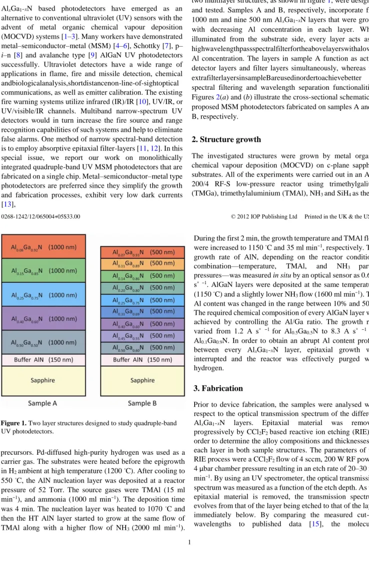
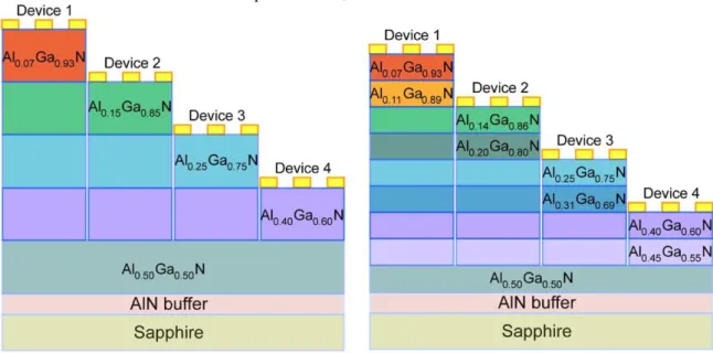
and allow for operation even in the deep UV [14]. In this work, two multilayer structures, as shown in figure 1, were designed and tested. Samples A and B, respectively, incorporate five 1000 nm and nine 500 nm AlxGa1−xN layers that were grown with decreasing Al concentration in each layer. When illuminated from the substrate side, every layer acts as a highwavelengthpassspectralfilterfortheabovelayerswithalower Al concentration. The layers in sample A function as active detector layers and filter layers simultaneously, whereas the extrafilterlayersinsampleBareusedinordertoachievebetter spectral filtering and wavelength separation functionalities. Figures 2(a) and (b) illustrate the cross-sectional schematic of proposed MSM photodetectors fabricated on samples A and B, respectively.
2. Structure growth
The investigated structures were grown by metal organic chemical vapour deposition (MOCVD) on c-plane sapphire substrates. All of the experiments were carried out in an AIX 200/4 RF-S low-pressure reactor using trimethylgalium (TMGa), trimethylaluminium (TMAl), NH3 and SiH4 as the
0268-1242/12/065004+05$33.00 © 2012 IOP Publishing Ltd Printed in the UK & the USA
Figure 1. Two layer structures designed to study quadruple-band UV photodetectors.
precursors. Pd-diffused high-purity hydrogen was used as a carrier gas. The substrates were heated before the epigrowth in H2 ambient at high temperature (1200 ◦C). After cooling to 550 ◦C, the AlN nucleation layer was deposited at a reactor pressure of 52 Torr. The source gases were TMAl (15 ml min−1), and ammonia (1000 ml min−1). The deposition time was 4 min. The nucleation layer was heated to 1070 ◦C and then the HT AlN layer started to grow at the same flow of TMAl along with a higher flow of NH3 (2000 ml min−1).
During the first 2 min, the growth temperature and TMAl flow were increased to 1150 ◦C and 35 ml min−1, respectively. The growth rate of AlN, depending on the reactor conditions combination—temperature, TMAl, and NH3 partial pressures—was measured in situ by an optical sensor as 0.6 A s˚ −1. AlGaN layers were deposited at the same temperature (1150 ◦C) and a slightly lower NH3 flow (1600 ml min−1). The Al content was changed in the range between 10% and 50%. The required chemical composition of every AlGaN layer was achieved by controlling the Al/Ga ratio. The growth rate varied from 1.2 A s˚ −1 for Al
0.5Ga0.5N to 8.3 A s˚ −1 for Al0.1Ga0.9N. In order to obtain an abrupt Al content profile between every AlxGa1−xN layer, epitaxial growth was interrupted and the reactor was effectively purged with hydrogen.
3. Fabrication
Prior to device fabrication, the samples were analysed with respect to the optical transmission spectrum of the different AlxGa1−xN layers. Epitaxial material was removed progressively by CCl2F2 based reactive ion etching (RIE) in order to determine the alloy compositions and thicknesses of each layer in both sample structures. The parameters of the RIE process were a CCl2F2 flow of 4 sccm, 200 W RF power, 4 μbar chamber pressure resulting in an etch rate of 20–30 nm min−1. By using an UV spectrometer, the optical transmission spectrum was measured as a function of the etch depth. As the epitaxial material is removed, the transmission spectrum evolves from that of the layer being etched to that of the layer immediately below. By comparing the measured cut-off wavelengths to published data [15], the molecular
Semicond. Sci. Technol. 27 (2012) 065004 M Gokkavas¨ et al
composition of each layer is determined. Figure 1 shows the measured compositions for samples A and B. The thicknesses of each layer were determined to be in accordance with the design values of 1000 nm and 500 nm for samples A and B,
respectively, within a 5% error associated with the thickness measurement, which is a consequence of the stepwise nature of the progressive etching process.
(a) (b)
Figure 2. Cross-section of proposed device structure, demonstrating the recess etching and positioning of metal contacts for four devices fabricated on samples A (a) and B (b).
Semicond. Sci. Technol. 27 (2012) 065004 M Gokkavas¨ et
al
3 Figure 3. Conceptional drawing (a) and photomicrograph (b) of quadruple-band MSM photodetectors.
For the fabrication of the monolithically integrated quadruple-band photodetectors as illustrated in figure 2, the sample surface was lithographically protected and etched during a series of RIE steps: For the first etch step, the 1st quadrant area was protected and etching was stopped when the depth reached the desired value for the second detector. Similarly, for the second etch step, the 1st and 2nd quadrant areas were protected; and finally, for the third etch step, all the quadrants except the 4th quadrant were protected and the etching was completed when the desired depth for the fourth detector was reached. For sample A, each quadrant was recess etched in order to fabricate one detector on each of the top four layers of the structure. In comparison, for sample B, each quadrant was recess etched to every other layer starting with the top layer. The spacer layers between the actual photodetector layers were reserved as spectral filters when fabricating sample B. On the as-grown and three staircase-like etched quadrants of the quadruple photodetector area, MSM photodetectors were fabricated by the deposition of 100 A Pt˚ /2000 A Au finger metallization˚ in a single step. The width and spacing of the interdigitated fingers were 3 μm, and the device active areas and probe-pads were 180 μm × 180 μm. A conceptional three-dimensional drawing and a photomicrograph of the completed quadruple photodetector are shown in figures 3(a) and (b), respectively. The arrangement of one detector on each quadrant allows for the uniform illumination through a circularly symmetric light probe such as a fibre or a laser beam.
4. Results
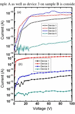
Figure 4 shows the measured dark current in the 0–100 V range for the fabricated photodetectors. Breakdown was not observed in this range, which was limited by our measurement equipment. All of the devices exhibited good dark current characteristics below the level of 10−10 A, with the only exception being device 2 on sample B, which had dark current on the order of 10−8 A. It is expected to observe lower dark current for higher Al concentration layers as a result of the larger bandgap. This expectation was met only for devices 4 on both samples. In contrast, for both samples, devices 1 had lower dark current compared to devices 2 and 3, which indicates an increase in dark current as a result of the plasma etch process. Nevertheless, the 2 orders of magnitude higher
dark current of device 2 on sample B compared to devices 2– 3
on sample A as well as device 3 on sample B is considered to
Figure 4. Current–voltage characteristics of quadruple-band photodetectors that were fabricated on samples A (a) and B (b). be related to epitaxial sample quality. This is supported by the observation that, for the devices 1, 3 and 4, the dark current was comparable on corresponding devices on both samples, whereas devices 2 on sample A and B are the only exception to this trend. The exact nature of this discrepancy between the two samples is beyond the scope of this work and is not further investigated.
The spectral responsivity of the fabricated devices was measured by using a Xe lamp and monochromator assembly. Themonochromator
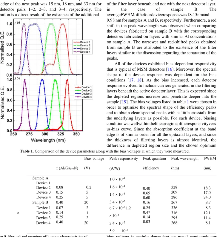
outputwascoupledintoamultimodeUVenhanced fibre and delivered through the substrate (backside illumination) of the device under test on a probe station. The spectral power density of the light at the output of the fibre probe was measured by a calibrated Si photodetector. The quantum efficiency of all four devices on both samples is plotted in figure 5 for the 250–375 nm spectral range. For an improved visualization of the spectral shape of the response, the quantum efficiency of each detector was normalized to the value at the respective peak wavelength. The exact value of the peak quantum efficiency, peak responsivity, peak wavelength, full-width at half-maximum (FWHM) of the quantum efficiency peak, and bias voltage at which the measurement was performed, are all listed in table 1 for each device. It was observed that the efficiency peaks were narrower and better separated for the devices on sample B
(a) (b)
(a)
Semicond. Sci. Technol. 27 (2012) 065004 M Gokkavas¨ et
al
4 compared to the devices on sample A. On sample B, the wavelength separation at the half-maximum normalized quantum efficiency between the red edge of one peak and the blue edge of the next peak was 15 nm, 18 nm, and 33 nm for the detector pairs 1–2, 2–3, and 3–4, respectively. The separation is a direct result of the existence of the additional
Figure 5. Normalized quantum efficiency characteristics of quadruple-band photodetectors that were fabricated on samples A (a) and B (b).
absorptive filter layers sandwiched between the detector active layers. In comparison, the peaks obtained from the devices on sample A are not separated at all. This result is expected since there are no filtering layers present in this sample and the detectors are fabricated on consecutive layers of the structure. The blue edge of each detector response coincides with the cut-off wavelength of the next layer
beneath, which is equal to the red edge of the detector response fabricated on that layer. In contrast, the blue edge of each detector response coincides with the cut-off wavelength of the filter layer beneath and not with the next detector layer,
in the case of sample B. The
averageFWHMofthefourdeviceresponseswas18.15nmand 9.98 nm for samples A and B, respectively. Furthermore, a red shift in the peak wavelength was observed when comparing the devices fabricated on sample B with the corresponding detectors fabricated on layers with similar Al concentrations on sample A. The narrower and red-shifted peaks obtained from sample B are attributed to the existence of the filter layers similar to the discussion regarding the separation of the peaks.
All of the devices exhibited bias-dependent responsivity that is typical of MSM detectors [16]. Moreover, the spectral shape of the device response was dependent on the bias conditions [17, 18]. As the bias increased, each detector response evolved to include carriers generated in the filtering layers beneath the active detector layer. This is expected since the depleted regions increase and penetrate deeper into the sample [19]. The bias voltages listed in table 1 were chosen in order to optimize the spectral shape of the efficiency peaks and to obtain clean spectral peaks with as little crosstalk from the underlying layers as possible. For each device, biasing conditionwaswellwithinthelinearregimeoftheresponsivityvers us-bias curve. Since the absorption coefficient at the band edge is of similar order for all the epitaxial layers, and since the thickness of filtering layers is almost identical, the difference in depleted region size and the chosen optimum
bias voltage is mainly dependent on metal–semiconductor
barrier and charge
trapsatthesurface.ThethickeractivelayersonsampleAallow for higher bias voltages without depletion of layers below. Therefore, the quantum efficiency was higher for the devices fabricated on sample A compared to the devices fabricated on sample B in agreement with thicker active layers. Moreover, on both samples, device 2 had the highest and device 4 had the lowest quantum efficiency. This indicates the existence of a defect-associated photoconductive gain, considering that Table 1. Comparison of the device parameters along with the bias voltages at which they were measured.
Bias voltage Peak responsivity Peak quantum Peak wavelength FWHM
x (AlxGa1−xN) (V) (A/W) efficiency (nm) (nm) Sample A Device 1 Device 2 Device 3 Device 4 Sample B 0.08 0.15 0.25 0.40 0.2 5 5 20 1.0 × 10⁻¹ 1.6 × 10⁻¹ 1.4 × 10⁻¹ 3.4 × 10⁻² 0.40 0.65 0.60 0.16 328 309 286 267 18.3 17.0 24.0 8.7 Device 1 Device 2 Device 3 Device 4 0.07 0.14 0.25 0.40 2 1 2 20 6.7 × 10⁻² 1.2 × 10⁻¹ 3.4 × 10⁻² 5.9 10−3 0.25 0.47 0.14 0.03 336 316 295 268 8.3 12.1 11.4 8.1 × (a) (b)
Semicond. Sci. Technol. 27 (2012) 065004 M Gokkavas¨ et
al
5 device 2 had the highest and device 4 had the lowest dark current on both samples, respectively.
5. Summary
Inspecting the device spectral responses in figure 5, and by comparing the layer structures, we arrive at the following conclusion: The shapes and positions of each spectral peak can be adjusted by design. The peaks can be made broad and flat-topped (as in device 3, sample A), or narrow by increasing or decreasing the compositional difference between the active detector layer and the filter layer directly beneath it, respectively. The position of the peaks can be selected by changing the compositions of both the detector and filter layers (as in all devices on sample B). The thickness of detector layers serves as separation between carriers generated in the filter layers and the depleted contact regions in conjunction with the applied bias. The thickness of the filter layers, on the other hand, serves to absorb the out-of band spectrum before it can enter the charge collection region of the detector. For a typical absorption coefficient of 1 × 105 cm−1, a 0.5 μm thick filter layer absorbs 99.4% of the out-of band spectrum. Therefore, the limiting factor for crosstalk between detector layer and filter layer is not optical, but the electrical isolation of carriers.
In conclusion, we designed, fabricated, and tested quadruple band UV MSM photodetectors on two AlGaN heterostructures. A comparison of the photoresponse shows that sample A, which incorporates five compositionally discrete layers, resulted in four distinct spectral peaks with no significant spectral separation, whereas sample B, which consists of nine discrete layers—four active device layers sandwiched between five spectral filter layers—yielded four narrower and well separated peaks as a result of absorption in the filter layers. The average of the FWHM of the quantum efficiency peaks was 18.15 nm for sample A and 9.98 nm for sample B. This result demonstrates that it is possible to obtain the desired spectral position, FWHM and peak-topeak separation by the incorporation of filter layers and the optimization of the layer compositions and thicknesses in the epitaxial structure.
Acknowledgments
This work is supported by the projects DPT-HAMIT, EUPHOME, EU-N4E, NATO-SET-181 and TUBITAK under project nos, 107A004, 107A012,109E301. One of the authors (E.O.) also acknowledges partial support from the Turkish Academy of Sciences.
References
[1] Razeghi M and Rogalsky A 1996 J. Appl. Phys. 79 7433 [2] Monroy E, Omnes F and Calle F 2003 Semicond. Sci. Technol.
18 R33
[3] Khan M A, Shatalov M, Maruska H P, Wang H M and Kuokstis E 2005 Japan. J. Appl. Phys. 1 44 7191
[4] Monroy E, Calle F, Munoz E and Omnes F 1999 Appl. Phys.
Lett. 74 3401
[5] Li T, Lambert D J H, Beck A L, Collins C J, Yang B, Wong J M M, Chowdhury U, Dupuis R D and Campbell J C
2000 Electron. Lett. 36 1581
[6] Gokkavas M, Butun S, Tut T, Biyikli N and Ozbay E 2007¨
Photonics Nanostruct. Fundam. Appl. 5 53
[7] Biyikli N, Kimukin I, Aytur O, Gokkavas M, Unlu M S¨ and Ozbay E 2001 Appl. Phys. Lett. 79 2838
[8] Collins C J, Chowdhury U, Wong M M, Yang B, Beck A L, Dupuis R D and Campbell J C 2002 Appl. Phys. Lett.
80 3754
[9] Tut T, Butun B, Gokkavas M and Ozbay E 2007¨
Photonics Nanostruct. Fundam. Appl. 5 140
[10] Reine M B et al 1995 J. Electron. Mater. 24 669
[11] Gokkavas M, Butun S, Yu H B, Tut T, Butun B and Ozbay E¨
2006 Appl. Phys. Lett. 89 143503
[12] Karrer U, Dobner A, Ambacher O and Stutzmann M 2000
J. Vac. Sci. Technol. B 18 757
[13] Butun S, Gokkavas M, Yu H B and Ozbay E 2006¨ Appl.
Phys. Lett. 89 073503
[14] Butun S, Tut T, Gokkavas M, Yu H B and Ozbay E 2006¨
Appl.
Phys. Lett. 88 123503
[15] Lee S R, Wright A F, Crawford M H, Petersen G A, Han J and Biefeld R M 1999 Appl. Phys. Lett.
74 3344
[16] Liou L C and Nabet B 1996 Appl. Opt. 35 15 [17] Gao B, Liu H, Fan J and Wang S 2011 IEEE Trans. Electron.
Devices 58 4290
[18] Korona K P, Drabinska A, Caban P and Strupinski W 2009
J. Appl. Phys. 105 083712
[19] Ohsawa J, Kozawa T, Miura H, Fujishima O and Itoh H 2005