Solution Processed Tungsten Oxide Interfacial Layer
for Effi cient Hole-Injection in Quantum Dot
Light-Emitting Diodes
Xuyong Yang , Evren Mutlugun , Yongbiao Zhao , Yuan Gao , Kheng Swee Leck ,
Yanyan Ma , Lin Ke , Swee Tiam Tan , Hilmi Volkan Demir ,* and Xiao Wei Sun *
Light-emitting diodes (LEDs) based on colloidal quantum dots (QDs) are highly promising for the next generation of lighting and displays thanks to their narrow emission linewidth, [ 1–4 ] tunable color emission spectral window across
the visible to near-infrared range, [ 5–7 ] and cost-effective
fabrication techniques compatible with solution processed methods. [ 8–12 ] Ever since the fi rst demonstration of
QD-based LEDs (QLEDs) 18 years ago, [ 13 ] rapid progress has
been made in the device performances owing to the tech-nological development and accumulation of relevant knowl-edge in materials and device architectures, i.e., understanding the underlying device physics, [ 14–16 ] designing more effi cient
device architectures, [ 17–20 ] and improving quantum dot
prop-erties by adjusting their composition and structure. [ 21–23 ] To
date, QLEDs have emerged as an undeniable competitor to organic light-emitting diodes (OLEDs) for lighting and dis-play applications. However, despite their apparent advan-tages, long-term stability of QLEDs is still a big concern for their practical applications.
Traditionally, polyethylene dioxythiophene:polystyrene sulfonate (PEDOT:PSS) is the most widely used buffer layer on an indium tin oxide (ITO) electrode for the fabrication of QLEDs. However, the aqueous PEDOT:PSS dispersion causes a side effect on the QLED stability due to its hygro-scopic nature as well as acidic nature corroding the ITO electrode, resulting in the reduction of device lifetime. [ 24,25 ]
Furthermore, compared with the inorganic material-based devices, the organic interfacial buffer layers have inferior thermal stability. Efforts to replace PEDOT:PSS with metal-oxides such as tungsten-, molybdenum-, nickel-, copper (I)-, rhenium-, or vanadium-oxides (WO 3 , MoO 3, NiO, Cu 2 O,
ReO 3 , or V 2 O 5) have gained signifi cant importance in the
recent years. [ 26–31 ] In particular, highly n-doped WO 3 and
MoO 3 exhibiting remarkably deep lying electronic states and
effi cient hole-injection into organic materials have been dem-onstrated. [ 32–35 ] However, their unique electronic properties
have so far been primarily achieved using thin fi lms made by high-cost thermal evaporation under vacuum, which presents disadvantages due to the cost issues and incompatibility with roll-to-roll scalable manufacturing. Additionally, it has been demonstrated that metal-oxide nanoparticles (NPs) as the interfacial buffer layers are often more effi cient as compared to their bulk counterparts. For example, ZnO nanoparticle fi lms as the electron transporting layers (ETLs) prepared by a sol–gel method have been introduced, resulting in all-solution-processed QLEDs with the maximum brightness values of 31 000 cdm −2 , 68 000 cdm −2 and 4200 cd m −2 for red,
green and blue devices, respectively, which are among the highest reported thus far. [ 8 ] Recently, Meyer's group reported
the preparation of solution-processed MoO 3 nanoparticle
fi lms where the MoO 3 was spin-coated on ITO from a
suspen-sion containing MoO 3 nanoparticles and a block copolymer
dispersing agent in xylene. [ 36 ] However, the fi lms require
an extra O 2 -plasma treatment to remove the polymeric
dis-persing agent to facilitate hole injection in the device and the
DOI: 10.1002/smll.201301199
Light-Emitting Diodes
X. Y. Yang, Dr. E. Mutlugun, Dr. Y. B. Zhao, K. S. Leck, Dr. S. T. Tan, Prof. H. V. Demir, Prof. X. W. Sun Luminous! Center of Excellence for Semiconductor Lighting and Displays,
School of Electrical and Electronic Engineering Nanyang Technological University
Nanyang Avenue, Singapore , 639798 , Singapore E-mail: [email protected]; [email protected] Dr. E. Mutlugun, Prof. H. V. Demir
Department of Electrical and Electronics Engineering Department of Physics, UNAM – Institute of Materials Science and Nanotechnology,
Bilkent University
Bilkent, Ankara , 06800 , Turkey Y. Gao, Prof. H. V. Demir
School of Physical and Mathematical Sciences Nanyang Technological University
Nanyang Avenue, Singapore , 639798 , Singapore Y. Y. Ma
State Key Lab of Luminescence Materials and Devices Institute of Optical Communication Materials South China University of Technology Guangdong , 510641 , China
Dr. L. Ke
Institute of Materials Research and Engineering A* STAR (Agency for Science, Technology and Research) 3 Research Link , Singapore , 117602 , Singapore Prof. X. W. Sun
South University of Science and Technology
communications
resulting surface of MoO 3 nanoparticle fi lm was relatively
rough. Therefore, as such, in-depth studies focusing on solu-tion-processed inorganic interfacial buffer layers is of critical importance for improving the QLED performance.
Here we report a highly effi cient, stable QLED using solu-tion-processed WO 3 nanoparticles as the hole injection layer.
The preparation of the WO 3 nanoparticle layer described here is simple and cost-effective employing cheap and com-mercially available WO 3 nanoparticles and ethanol as a
sol-vent and utilizing a low-temperature process under ambient conditions (annealing temperature can be as low as 80 °C and without requiring the O 2 -plasma treatment). This
treat-ment temperature is much lower than that of PEDOT:PSS (120–150 °C). At the same time, the overall performance for WO 3 nanoparticle-based QLED is superior compared to that of the present PEDOT:PSS-based QLEDs using the same device architecture. The WO 3 nanoparticle-based QLEDs
with a maximum brightness of 30, 006 cd/m 2, an external
quantum effi ciency (EQE) of 3.32%, and a peak current effi -ciency of 10.75 cd A −1 have been achieved. Besides, the device
lifetime has been also improved remarkably compared to that of PEDOT:PSS-based QLEDs, which marks as a further step towards the practical application of the QLED technology.
The standard structure of QLEDs is given as a multilayer structure of ITO/poly(3,4-ethylenedioxy-thiophene)poly(styrenesulfonate)(PEDOT:PSS)/Poly[ N , N ′-bis(4-butylphenyl)- N,N ′-bis(phenyl)benzidine] (poly-TPD)/ QDs/2, 2′, 2′′- (1, 3, 5-benzinetriyl)-tris(1-phenyl-1- H -ben-zimidazole) (TPBi)/LiF/Al). [ 17,22 ] The CdSe/ZnS core-shell
structured QDs prepared according to a previous reported literature were used for the emissive layer. [ 3 ] The poly-TPD
and TPBi layers were chosen as the hole transport layer (HTL) and the electron transport layer (ETL), respectively.
In our case, the WO 3 nanoparticle layer spin-coated on ITO
was used to replace PEDOT:PSS as the HIL. The device structure is schematically presented in Figure 1 a. The atomic force microscopy (AFM) image of the close-packed thin fi lm of WO 3 nanoparticles on ITO with an average particle size
of 7 nm (annealed at 100 °C in the glove box) is shown in Figure 1 b. The surface roughness (RMS) of the fi lm made from a 2 wt% of WO 3 ethanol solution is only 2.8 nm,
indi-cating that the nanoparticle fi lm has a smooth surface. To confi rm the electronic structure of the as-prepared WO 3
nanoparticle fi lm, the ultraviolet photoelectron spectroscopy (UPS) spectra including the magnifi ed regions of the pho-toemission cut-off and valence band are given in Figures 1 c and 1 d. The photoemission onset is found at 16.05 eV from the photoemission cut-off in Figure 1 c. This corresponds to a work function (WF) of 5.15 eV in agreement with the WF values of WO 3 reported in literature, which can range
from 4.7 to 6.4 eV depending on the fi lm preparation condi-tions. [ 37 ] Figure 1 d displays the zoom-in spectra of the density
of states near the oxide valence band edge and the ionization energy (IE) of the WO 3 fi lm that is determined to be 2.7 eV
with respect to the Fermi level. According to the schematic energy level diagram of the device depicted in Figure 1 e, it can be observed that the electrons can easily be injected from the Al to the QD layer. However, the case is quite dif-ferent for the hole injection. [ 24,34,36 ] Owing to the deep lying
electronic states of WO 3 nanoparticle interface layer, effi -cient hole injection can be proceeded via electron extraction from the highest occupied molecular orbital (HOMO) level of poly-TPD into the conduction band of WO 3 nanoparticles.
For n-doped WO 3 or MoO 3 , the hole injection from ITO to the organic semiconductors results from electron extraction from the highest occupied molecular orbital (HOMO) level
Figure 1. (a) Schematic of the device confi guration of the QLEDs. (b) AFM image of WO 3 nanoparticle HTL formed on ITO substrate. UPS spectra of a
WO 3 nanoparticle fi lm annealed at 100 °C including (c) secondary-electron cutoff and (d) zoom-in section of the evolution of the density of states
Solution Processed Tungsten Oxide Interfacial Layer for Effi cient Hole-Injection in Quantum Dot
of organic semiconductors through the WO 3 or MoO 3
con-duction band, and then into ITO. For our case, owing to the deep lying electronic states of WO 3 nanoparticle interface
layer, the energy barrier for the injection of electrons from the HOMO level of to the conduction band of WO 3
nano-particles is quite small, and the effi cient hole injection can be proceeded via electron extraction from the HOMO level of poly-TPD into the conduction band of WO 3 nanoparticles.
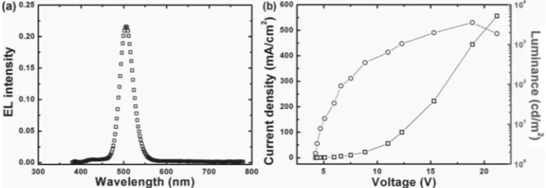
Figure 2 a presents the output performance of an optimized WO 3 nanoparticle-based QLED. The device is fabricated with QDs of 4 monolayers-equivalent thickness ( ∼ 20 nm) and a WO 3 nanoparticle fi lm of 2 monolayers-equivalent
thickness ( ∼ 14 nm). The electroluminescence (EL) spec-trum of the QLED was recorded at the bias voltage of 12 V, showing a characteristic QD EL peak centered at ∼ 518 nm with a full-width-at-half-maximum (FWHM) of ∼ 30 nm. It should be noted here that there is a weak emission in the blue-wavelength region due to the residual emission from poly-TPD. The emission from poly-TPD indicates the pos-sible imbalance of the charge in the QD layer. The elec-trons on the lowest unoccupied molecular orbital (LUMO) of TPBi can jump over the 0.9 eV energy barrier into the LUMO of poly-TPD through defects of the QD layer to combine with holes in the poly-TPD layer. This phenomenon can be observed in almost all PEDOT:PSS-based QLEDs. Figure 2 b shows the luminance and current density charac-teristics of the device as a function of the applied voltage. The luminance-current density-voltage characteristics show a low turn-on voltage of 3.6 V and a peak luminance of 3565 cd/m 2
at a current density of 444.44 mA/cm 2 . The maximum EQE
of 0.43% was obtained under the same current density. To further improve the performance of WO 3
nanoparticle-based QLEDs, we deposited a 2,2’,2”-tris-(N-carbazolyl)-triphenylamine (TCTA) electron-blocking layer (EBL) on the QD layer to suppress the excess electrons for improving the charge balance of device. The LUMO of TCTA is 2.4 eV [ 38 ]
and the relatively high energy barrier of 0.8 eV between the LUMO of TCTA and that of TPBi can block electrons to reach the poly-TPD layer in the device effectively. Figure 3 a shows the EL spectra for the device with TCTA utilized as the EBL under different driving currents. It can be observed that the blue emission of poly-TPD is hardly found even in the case of a high driving current, as electrons from TPBi are completely blocked by the TCTA EBL before jumping into
the LUMO of poly-TPD. This is another advantage of using TCTA because the blue emission from poly-TPD degrades the color purity. Compared with the original QLEDs without the TCTA used as the EBL, the performance of QLED with TCTA is increased signifi cantly, showing the maximum lumi-nance, EQE and current effi ciency values of 30 006 cd m −2
and 3.32%, respectively. To the best of our knowledge, the EQE of 3.32% is much higher than the previously reported values for green QLEDs with normal architecture (the recently reported green QLEDs using the inverted archi-tecture reached an EQE level of 5.8%). [ 17 ] A corresponding
image of the QLED output was recorded at the luminance of 300 cd/m 2 , which displays bright and saturated green
emis-sion (Figure 3 b). Figures 3 c and 3 d show a comparison of the luminance-current density ( L – J ) and effi ciency-current density ( E–J ) characteristics of the WO 3 nanoparticle-based
QLED and an optimized PEDOT:PSS-based QLED with the same structure. As can be seen, the two devices show a similar trend in the L–J and E–J characteristics, as the driving current is increased. Table 1 summarizes the key fi gures of the two QLEDs. The maximum brightness, EQE, current effi -ciency and effi cacy for the WO 3 nanoparticle-based QLED are superior. Also, the turn-on voltage of the WO 3
nanopar-ticle-based QLED decreases to 3.8 V, which is lower than that observed for the PEDOT:PSS-based device (4.2 V). Moreover, it can be noted that the WO 3 nanoparticle-based QLED still works well even under the current of 50 mA, while the PEDOT:PSS-based QLED has burned down when the driving current is just 40 mA, which indicates the better device stability for the WO 3 nanoparticle-based QLED.
Figure 4 shows the operating stability of the resulting unencapsulated WO 3 nanoparticle-based QLED in
compar-ison with the optimized PEDOT:PSS-based QLED. Under a continuous current driving condition corresponding to an initial luminance of 1000 cd/m 2 , it can be clearly observed
that using WO 3 nanoparticles to replace PEDOT:PSS as the
HILs in QLEDs can drastically improve device stability. The unencapsulated WO 3 nanoparticle-based QLED displays a half-lifetime of ca. 6530 s, showing an approximately two-fold lifetime enhancement as compared to that of PEDOT:PSS-based QLED. The signifi cant improvement in the device sta-bility can be attributed to the fact that WO 3 nanoparticles are highly stable when compared to organic materials and can therefore act as a protection layer for organic materials.
communications
In summary, we have demonstrated an effi cient QLED using solution-processed WO 3 nanoparticle fi lm instead of
using PEDOT:PSS as the anode interfacial buffer layer. The WO 3 nanoparticle-based QLEDs show enhanced perfor-mance as compared to the PEDOT:PSS-based QLEDs. The EQE of 3.32% reported here is the highest value for green QLEDs using a non-inverted structure and the brightness of 30 006 cd/m 2 matches that of the best QLEDs with organic
materials used as HTLs/HILs. Moreover, with the incorpo-ration of the WO 3 nanoparticles, the unencapsulated device
exhibits a signifi cant improvement in the device stability and the lifetime is increased by approximately two-folds at
an initial brightness of 1000 cd/m 2 as compared to that of
PEDOT:PSS-based QLED. Meanwhile, since the solution-processed preparation method of WO 3 nanoparticle fi lm
used in our work is very simple and can be achieved at low annealing temperatures, it is suitable for application in fl ex-ible devices where the fl exex-ible substrates such as plastics often cannot withstand high annealing temperatures. These results indicate that WO 3 nanoparticles are promising solu-tion-processed buffer layer materials and offer a practicable platform for the realization of high-performance, stable and large-area commercial QLEDs using a low-cost manufac-turing process.
Figure 3. (a) EL spectra of the device at different injection currents (inset shows the schematic cross section of the device structure used in this study). (b) The photograph of a QLED under operation with a pixel size of 3 mm×3 mm. (c) Luminance (cd m −2 ) and (d) external quantum effi ciency
(%) of QLEDs using PEDOT:PSS and WO 3 nanoparticles as the HTLs as a function of current density (mA cm −2 ).
Table 1. List of fi gure-of-merits to compare the device performance using WO 3 nanoparticles (A) and PEDOT:PSS (B) as HILs.
Device Vturn-on [V] Max. Luminance [cd/m 2 ] Max. EQE [%]
Max. Current effi ciency [cd/A]
Max. Effi cacy [lm/W]
Lifetime [s]
A 3.8 30 006 (@50 mA) 3.32 9.75 6.8 6530
Solution Processed Tungsten Oxide Interfacial Layer for Effi cient Hole-Injection in Quantum Dot
Experimental Details
Synthesis of ZnS Core–Shell QDs : Green-emitting CdSe-ZnS QDs with a chemical-composition gradient were prepared according to a modifi ed method reported in the literature. [ 3 ] For a
typical preparation of green-emitting QDs, 0.1 mmol of cadmium oxide (CdO), 4 mmol of zinc acetate (Zn(Acet) 2), 5 mL of oleic acid (OA) were loaded in a 50 mL 3-neck fl ask, heated to 150 °C under vacuum to form cadmium oleate (Cd(OA) 2 ) and zinc oleate (Zn(OA) 2 ). Then 20 mL of 1-octadecene (1-ODE) was added to the reaction fl ask and the reactor was then fi lled with nitrogen and heated up to 300 °C. At the elevated temperature, 1.6 mL of tri-n-octylphosphine (TOP) dissolving 0.15 mmol of selenium (Se) and 4 mmol of sulphur (S) was injected into the fl ask swiftly, and the reaction mixture were maintained at 300 °C for 10 min for the QD growth. To purify the synthesized QDs, the reaction mixture was cooled down to room temperature, and the QDs were extracted by the addition of acetone and methanol, followed by centrifugation. The CdSe-ZnS core-shell QDs were readily dispersed in toluene.
Fabrication of QLED Devices : The patterned ITO substrates were cleaned by sonication sequentially in detergent, de-ionized water, acetone, and isopropyl alcohol. The WO 3 anode buffer layer was spin-coated on the O 2 -plasma treated ITO substrate from diluted 1.25 wt% of WO 3 enthanol solution at 5000 rpm for 60 s and annealed at 80–110 °C for 30 min. The 2 wt% of poly-TPD (50 nm) in chlorobenzene was also spin-coated on the WO 3 layer at 4000 rpm for 60 s, followed by thermal annealing at 150 °C for 30 min in a nitrogen glove box. The QD layer was then deposited on the ITO/WO 3 /poly-TPD layer by spin-coating the QD dispersion (QDs were dispersed in toluene with 15 mg/mL) at a rate of 1000– 4000 rpm for 60 s, and cured at 90 °C under N 2 atmosphere for 30 min. The TPBi (35 nm), LiF (0.5 nm), and Al (190 nm) layers were thermally deposited under a base pressure of ∼ 2 × 10 −4 Pa.
WO 3 dispersion in enthanol (2.5 wt%) was purchased from Nano-grade GmbH (product no. 4035). For PEDOT:PSS based QLEDs, we
followed the same procedure and only the WO 3 layer was replaced by PEDOT:PSS layer (40 nm) which was spun on the ITO substrate at 4000 rpm for 60 s and annealed at 150 °C for 30 min.
Instrumentation : AFM (Cypher AFM, Asylum Research) was used to image the WO 3 nanoparticle fi lm. UPS was performed using X-Ray Photoelectron spectroscopy (XPS) (VG Escalab 220i XL) with a He I (21.2 eV) gas discharge lamp. The electrolumines-cence (EL) spectra of the fabricated devices were measured using a PR650 Spectra Scan spectrometer, while the luminance-current density-voltage (L-J-V) characteristics were obtained simultane-ously, by connecting the spectrometer to a programmable Keithley 236 source measurement unit. All measurements were carried out at room temperature under ambient conditions.
Acknowledgments
The authors would like to thank the fi nancial support from Singa-pore National Research Foundation under NRF-RF-2009–09 and NRF-CRP-6–2010–02 and the Science and Engineering Research Council, Agency for Science, Technology and Research (A*STAR) of Singapore (project Nos. 092 101 0057 and 112 120 2009). The work is also supported by the National Natural Science Foundation of China (NSFC) (project Nos. 61006037 and 61076015).
[1] Y. Shirasaki , G. J. Supran , M. G. Bawendi , V. Bulovic´ , Nat.
Pho-tonics 2013 , 7 , 13 – 23 .
[2] K. S. Cho , E. K. Lee , W. J. Joo , E. Jang , T. H. Kim , S. J. Lee , S. J. Kwon , J. Y. Han , B. K. Kim , B. L. Choi1 , J. M. Kim , Nat.
Pho-tonics 2009 , 3 , 341 – 345 .
[3] W. K. Bae , J. Kwak , J. Lim , D. Lee , M. K. Nam , K. Char , C. Lee , S. Lee , Nano Lett. 2010 , 10 , 2368 – 2373 .
[4] V. Wood , V. Bulovic´ , Nano Rev. 2010 , 1 , 5202 – 5208 .
[5] X. Yang , D. Zhao , K. S. Leck , S. T. Tan , Y. X. Tang , J. Zhao , H. V. Demir , X. W. Sun , Adv. Mater. 2012 , 24 , 4180 – 4185 . [6] P. O. Anikeeva , J. E. Halpert , M. G. Bawendi , V. Bulovic´ , Nano Lett.
2009 , 9 , 2532 – 2536 .
[7] L. Sun , J. J. Choi , D. Stachnik , A. C. Bartnik , B.-R. Hyun , G. G. Malliaras , T. Hanrath , F. W. Wise , Nat. Nanotechnol. 2012 , 7 , 369 – 373 .
[8] L. Qian , Y. Zheng , J. Xue , P. H. Holloway , Nat. Photonics 2011 , 5 , 543 – 548 .
[9] Y. Zhang , C. Xie , H. Su , J. Liu , S. Pickering , Y. Wang , W. W. Yu , J. Wang , Y. Wang , J. I. Hahm , N. Dellas , S. E. Mohney , J. Xu , Nano
Lett. 2011 , 11 , 329 – 332 .
[10] M. A. Schreuder , K. Xiao , I. N. Ivanov , S. M. Weiss , S. J. Rosenthal , Nano Lett. 2010 , 10 , 573 – 576 .
[11] Z. Tan , F. Zhang , T. Zhu , J. Xu , A. Y. Wang , J. D. Dixon , L. Li , Q. Zhang , S. E. Mohney , Nano Lett. 2007 , 7 , 3803 – 3807 . [12] Z. Tan , Y. Zhang , C. Xie , H. Su , J. Liu , C. Zhang , N. Dellas ,
S. E. Mohney , Y. Wang , J. Wang , J. Xu , Adv. Mater. 2011 , 23 , 3553 – 3558 .
[13] V. L. Colvin , M. C. Schlamp , A. P. Alivisatos , Nature 1994 , 370 , 354 – 357 .
[14] D. Bozyigit , O. Yarema , V. Wood , Adv. Funct. Mater. 2013, doi: 10.1002/adfm.201203191 .
[15] X. Yang , Y. Divayana , D. Zhao , K. S. Leck , F. Lu , S. T. Tan , A. P. Abiyasa , Y. Zhao , H. V. Demir , X. W. Sun , Appl. Phys. Lett. 201 2 , 101 , 233110 – 233113 .
Figure 4. Operational lifetime characteristics of the resulting WO 3
nanoparticle based QLED and the optimized PEDOT:PSS based QLED. The luminance of these QLEDs was measured without using encapsulation and during the continuous operation at a constant current density corresponding to an initial luminance of 1000 cd/m 2 . Both types of
communications
[16] M. L. Mastronardi , E. J. Henderson , D. P. Puzzo , Y. Chang , Z. B. Wang , M. G. Helander , J. Jeong , N. P. Kherani , Z. Lu , G. A. Ozin , Small 2012 , 12 , 3647 – 3654 .
[17] J. Kwak , W. K. Bae , D. Lee , I. Park , J. Lim , M. Park , H. Cho , H. Woo , D. Y. Yoon , K. Char , S. Lee , C. Lee , Nano Lett. 2012 , 12 , 2362 – 2366 .
[18] V. Wood , M. J. Panzer , J. M. Caruge , J. E. Halpert , M. G. Bawendi , V. Bulovic´ , Nano Lett. 2010 , 10 , 24 – 29 .
[19] E. M. Likovich , R. Jaramillo , K. J. Russell , S. Ramanathan , V. Narayanamurti , Adv. Mater. 2011 , 23 , 4521 – 4525 .
[20] Q. Sun , G. Subramanyam , L. Dai , M. Check , A. Campbell , R. Naik , J. Grote , Y. Wang , ACS Nano 2009 , 3 , 737 – 743 .
[21] B. N. Pal , Y. Ghosh , S. Brovelli , R. Laocharoensuk , V. I. Klimov , J. A. Hollingsworth , H. Htoon , Nano Lett. 2012 , 12 , 331 – 336 . [22] W. K. Bae , J. Kwak , J. W. Park , K. Char , C. Lee , S. Lee , Adv. Mater.
2009 , 21 , 1690 – 1694 .
[23] B. Chen , H. Zhong , W. Zhang , Z. Tan , Y. Li , C. Yu , T. Zhai , Y. Bando , S. Yang , B. Zou , Adv. Fun. Mater. 2012 , 22 , 2011 – 2088 . [24] S. Murase , Y. Yang , Adv. Mater. 2012 , 24 , 2459 – 2462 .
[25] J. J. Jasieniak , J. Seifter , J. Jo , T. Mates , A. J. Heeger , Adv. Funct.
Mater. 2012 , 22 , 2594 – 2605
[26] M. T. Greiner , M. G. Helander , W.-M. Tang , Z.-B. Wang , J. Qiu , Z.-H. Lu , Nat. Mater. 2012 , 11 , 76 – 81 .
[27] J. M. Caruge , J. E. Halpert , V. Wood , V. Bulovic´ , M. G. Bawendi , Nat. Photonics 2008 , 2 , 247 – 250 .
[28] Z. Tan , L. Li , C. Cui , Y. Ding , Q. Xu , S. Li , D. Qian , Y. Li , J. Phys.
Chem. C 2012 , 116 , 18626 – 18632 .
[29] H. M. Wei , H. B. Gong , L. Chen , M. Zi , B. Q. Cao , J. Phys. Chem. C 2012 , 116 , 10510 – 10515 .
[30] J. Meyer , K. Zilberberg , T. Ried , A. Kahn , J. Appl. Phys. 2011 , 110 , 033710 – 033714 .
[31] J.-H. Lee , D.-S. Leema , H.-J. Kim , J.-J. Kim , Appl. Phys. Lett. 2009 , 94 , 123306 – 123308 .
[32] M. Sessolo , H. J. Bolink , Adv. Mater. 2011 , 23 , 1829 – 71845 . [33] R. Acharya , X. A. Cao , Appl. Phys. Lett. 2012 , 101 , 053306 – 053309 . [34] M. Kröger , S. Hamwi , J. Meyer , T. Riedl , W. Kowalsky , A. Kahn ,
Appl. Phys. Lett. 2009 , 95 , 123301 – 123303 .
[35] Z. B. Wang , M. G. Helander , J. Qiu , D. P. Puzzo , M. T. Greiner , Z. M. Hudson , S. Wang , Z. W. Liu , Z. H. Lu , Nat. Photonics 2011 , 5 , 753 – 757 .
[36] J. Meyer , R. Khalandovsky , P. Görrn , A. Kahn , Adv. Mater. 2011 , 23 , 70 – 73 .
[37] S. Han , W. S. Shin , M. Seo , D. Gupta , S.-J. Moon , S. Yoo , Org.
Elec-tron. 2009 , 10 , 791 – 797 .
[38] J. Y. Lee , M.-S. Gong , S. Ryu , G.-k. Chang , H. J. Chang , J. Appl.
Phys. 2008 , 103 , 054502 – 054505 .
Received: April 19, 2013 Revised: May 27, 2013 Published online: