USES MATHEMA;riCAL MORPHOLOGICAL- IMASE
■; PROCESSJl^iG ALGORITHMS
■ : Jrr: ■ i uyik .;-r"
,r%rw w ^ i i··
liw'J -J UiSJUww ♦ .« -»«¡r'. #;;;w v·*,'«Si-i· •J w ■*; V’ '·. «w v v v· « vj ¿ii·’-· ■·· ·-» >
'rs ._ ./·%.. ;r·^ '''*■■·. i·^«» :. i "i“
= >·■■ A /Afi· ,'**·'· · ^.·?*· Vv·^.’ ■ ■·»;■"'· ·.■■ .
AN AUTOMATED RULE BASED VISUAL PRINTED
CIRCUIT BOARD INSPECTION SYSTEM WHICH
USES MATHEMATICAL MORPHOLOGICAL IMAGE
PROCESSING ALGORITHMS
A T H E S I S S U B M I T T E D T O T H E D E P A R T M E N T O F E L E C T R I C A L A N D E L E C T R O N I C S E N G I N E E R I N G A N D T H E I N S T I T U T E O F E N G I N E E R I N G A N D S C I E N C E S O F B I L K E N T U N I V E R S I T Y I N P A R T I A L F U L F I L L M E N T O F T H E R E Q U I R E M E N T S F O R T H E D E G R E E O F M A S T E R O F S C I E N C EBy
Seyfullah Halit Oğuz
February, 1990
U
©Copyright February 1990
by
I certify that I have read this thesis and that in my opinion it is fully adequate, in scope and in quality, as a thesis for the degree of Master of Science.
Assoc. Prof. Dr. Levent Onural (Principal Advisor)
I certify that I have read this thesis and that in my opinion it is fully adequate, in scope and in quality, as a thesis for the degree of Master of Science.
Prof.^Dr. Abdullah Atalar
I certify that I have read this thesis and that in my opinion it is fully adequate, in scope and in quality, as a thesis for the degree of Master of Science.
Assist. Prof. Dr. A. Enis Çetin
Approved for the Institute of Engineering and Sciences:
¿ ¿ ' ‘ 7 Prof. Dr. M e h m ^ Bar ay
IV
To my family, Hatice Ergil,
Güler Oğuz, Rüştü Oğuz, Kemal Oğuz, Zinnur Doğanata, Yurdaer Doğanata,
and ali other members,
A N A U T O M A T E D RULE BASED VISUAL PR IN TE D
CIRCUIT BO ARD INSPECTION SY ST E M W H IC H USES
M A TH E M A T IC A L M O R PH O LO G ICAL IM AG E
PROCESSING ALG O RITH M S
Seyfullali Halit Oğuz
M.S. in Electrical and Electronics Engineering
Supervisor: Assoc. Prof. Dr. Levent Onural
February, 1990
In this thesis, the design and implementation of an automated rule based visual printed circuit board (PCB) inspection system are presented. The developed system makes use of mathematical morphology based image processing algorithms. This system is designed for the detection of the PCB defects related to the conducting structures on the PCBs. For this purpose, four new algorithms, three of which are defect detection algorithms, are designed, and an already existing algorithm is modified for its implementation in our system. The designed defect detection algorithms respectively verify the minimum conductor trace width, minimum land width, and the minimum conductor trace spacing requirements on digital binary PCB images. The implementation of a prototype system is made in our image processing laboratory and the necessary computer programs are developed. These programs control the image processor and apply the defect detection algorithms to discrete binary PCB test images.
Keywords. Printed circuit boards, rule based systems, automated visual inspection, mathematical morphology.
ÖZET
M A T E M A T İK SE L M ORFOLOJİ K Ö K E N Lİ G Ö R Ü N T Ü
İŞLEME A L G O R İT M A L A R I K U L L A N A N BİR O T O M A T İK
K U R A L A DAYALI G Ö R Ü N TÜ SEL BASKILI D E V R E
K AR TI İNCELEM E SİSTEM İ
Seyfullah Halit Oğuz
Elektrik ve Elektronik Mühendisliği Bölümü Yüksek Lisans
Tez Yöneticisi: Doç. Dr. Levent Onural
Şubat, 1990
Ö ZET
Bu tez çalışmasında, baskılı devre kartlarının (PCB) hata tesbitini kurala dayalı olarak yapabilen otomatik bir görüntüsel inceleme sisteminin tasarımı ve gerçekleştirilmesi ele alınmıştır. Gerçekleştirilen sistem matematiksel morfolojiye dayalı görüntü işleme algoritmalarını kullanmaktadır. Söz konusu bu sistem, esas olarak baskılı devre kartlarının üzerindeki iletken yapılarla ilgili hataları bulmak üzere tasarlanmıştır. Bu amaçla, üç tanesi hata tesbiti algoritması olmak üzere, yeni dört tane algoritma geliştirilmiş ve var olan bir algoritma da sistemimizde kullanılabilmesi amacıyla uygun şekilde değiştirilmiştir. Geliştirilen hata tesbiti algoritmaları, baskılı devre kartlarından alınan kesikli ve iki seviyeli görüntüler üzerinde sırasıyla minimum iletken hat kalınlığı, minimum iletken bilezik kalınlığı ve iletken hatlar arası minimum uzaklık şartlarının sağlanıp sağlanmadıklarını kontrol etmektedir. Bir prototip sistem modeli görüntü işleme laboratuvarımızda kurulmuş ve gerekli sistem yazılımları geliştirilmiştir. Bu yazılımlar laboratuvanmızdaki görüntü işleme birimini kontrol eder ve hata tespit algoritmalarını kesikli ve iki seviyeli baskılı devre kartı test görüntülerine uygular.
Anahtar sözcükler. Baskılı devre kartları, kurala dayalı sistemler, otomatik görüntüsel inceleme, matematiksel morfoloji.
I am indebted to Assoc. Prof. Dr, Levent Onural for his encouragement, guidance, and invaluable suggestions during ray study.
I would also like to gratefully acknowledge the other members of my M.S. the.sis committee: Prof. Dr. Abdullah Atalar and Assist. Prof. Dr.
Ahmet Enis Çetin.
Finally, it is my pleasure to express my thanks to my friends, particularly Göüde Bozdağı, Mehmet İzzet Gürelli, Mustafa Karaman, Oğan Ocah, and Mehmet Tankut Özgen who made life easier for me during this study by'their continuous encouj'agement and some Vidiiable discussion.s.
Contents
1 Automated Visual Inspection of Printed Circuit Boards 1
1.1 Introduction... 1
1.2 Industrial Inspection Problem In G en eral... 1
1.3 Industrial Visual Inspection P r o b le m ... 2
1.4 Automated Visual Inspection ... 3
1.5 Automated Visual Inspection of Printed Circuit B o a r d s ... 6
1.6 Typical Defects Met on Printed Circuit B oards... 7
1.7 Printed Circuit Board Defects Related to the Conducting S tru ctu res... 8
1.7.1 Defining terms ... 9
1.7.2 Printed Circuit Board Defects Related to the Conducting S tru ctu res... 9
2 Mathematical Morphology and Its Fundamental Definitions 20 2.1 Introduction... 20
2.2 An Overview of Mathematical M orp h olog y ... 21
2.2.1 A Brief History of Mathematical Morphology 21
2.2.2 Basic Features of Mathematical M o rp h o lo g y ... 21
2.3 Fundamental Definitions of Digital Topology and the Adopted N o ta tio n ... 23
2.3.1 Fundamental Definitions of Digital Binary Image Topology 24
2.3.2 Adopted N otation... 29
2.4 Basic Morphological Operations and Some Related Fundamental P ropositions... 30
2.4.1 Basic Morphological O pera tion s... 30
2.4.2 Three Important Properties of Morphological Operations 36
2.5 Two Fundamental Morphological A lgorithm s... 39
2.5.1 The Symmetrical Thinning .Algorithm 40
2.5.2 The Pruning Algorithm ... 45
3 System Implementation 50
3.1 Introduction... 50
3.2 Application of Morphological Techniques to the Visual Inspec tion Problem and the Implementation of the Prototype System M o d e l ... 51
3.3 An Overview of the Imaging Technology Series 151 Image
Processor ... 56
3.4 System Software... 58
3.4.2 Utility P r o g r a m s ... 62
3.5 Running the S y s t e m ... 63
4 Defect Detection Algorithms 67 4.1 Introduction... 67
4.2 Isotropic Dilation and Erosion Structuring Elements for Rectan gularly Sampled Images with Different Horizontal and Vertical Sampling P e r io d s ... 69
4.3 The Algorithm Used for Removing the Holes and Their Surrounding Lands from the Digital I m a g e ... 77
4.4 The Algorithm for Verifying the Minimum Conductor Spacing Requirement... 83
4.5 The Algorithm for Verifying the Minimum Conductor Trace Width Requirement... 88
4.6 The Algorithm for Verifying the Minimum Land Width Require ment ... 93
4.7 The Modified Algorithm Designed to Supersede the Algorithms of Sections 4.4 and 4 . 5 ... 99
4.8 The Implementation of Morphological Operators Using 3x3 2-D Convolution and Table Lookup O peration s...110
5 Results and Conclusion 116 5.1 An Overview ...116
5.2 The Most Important Features of the Developed S y s te m ...117
5.3 Future W o rk ... 120
A Program L istin g s... 126
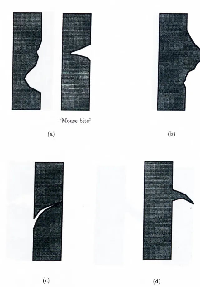
1.1 Small area defects, (a) intrusion, (b) protrusion, (c) scratch, (d) gouge, (e) splash, (f) pinhole, (g) open circuit, (h) short circuit. 11
1.2 Non-local defects, (a) missing circuitry, (b) non-local defects
resembling small area defects on a large scale... 14
1.3 Proximity defects, (a) local violation, (b) sustained violation. . . 15
1.4 Defects related to conductor trace width requirements, (a) violation of minimum trace width requirement, (b) violation of maximum trace width requirement... 16
1.5 Two examples of acute angle violation defects... 18
1.6 Defects related to the minimum land width requirement, (a) misregistration of the hole, (b) an intrusion on the land. . . . . 19
2.1 8-neighbors of a pixel. ... 26
2.2 4-neighbors of a pixel... 26
2.3 Examples of skeletal elements... 28
2.4 Examples of T-joins... 28
2.5 Example for Hit or Miss transformation, (a) original image, (b) the structuring element to be used, (c) result of the transformation. 32
2.6 Example for erosion operation, (a) original image, (b) the structuring element to be used, (c) the result of the erosion operation...
34
2.7 Example for dilation operation, (a) original image, (b) the structuring element to be used, (c) the result of the dilation operation...
37
2.8 Symmetrical thinning structuring elements, (a) for horizontal and vertical component thinning, (b) for inclined component and corner thinning... 41
2.9 Example for symmetrical foreground thinning until idem-potance, (a) original image, (b) result of symmetrical thinning until idempotance... 43
2.10 Example for symmetrical foreground thinning, (a) original image, (b) result of applying
12
steps of symmetrical thinning. .44
2.11 Example for symmetrical background thinning, (a) original image, (b) result of applying 9 steps of symmetrical thinning to background pixels... 46
2.12 Pruning structuring elements... '. . . 47
2.13 Example for foreground pruning, (a) original image, (b) result of applying 12 steps of pruning... 48
2.14 Example for background pruning, (a) original image, (b) result of applying 9 steps of pruning to background pixels... 49
3.1 The basic equipment of our image processing laboratory... 55
4.1
Checking for a common minimum width requirement on the foreground components of an analog binary image... 694.2 Discrete approximations to circular structures, (a ),(c),(d ),(e) discrete approximations to circular structures with diameters 3,5,7, and 9 pixels respectively, (b) the structuring element used initially by the algorithm of Section 4.2. 71
4.3 The structuring elements used by the algorithm of Section 4.2 to generate discrete approximations to circular structures with diameters corresponding to an odd number of pixels. 73
4.4 The structuring element used b}^ the algorithm of Section 4.2 to generate discrete approximations to circular structures with
diameters corresponding to an even number of pi.xels... 73
4.5 A discrete approximation to an elliptic structure, (a) the structuring element, (b) decomposition of the structuring element. 76 4.6 Another discrete approximation to an elliptic structure, (a) the structuring element, (b) decomposition of the structuring element. 78 4.7 Example for the algorithm of Section 4.3... 79
4.8 Example for the algorithm of Section 4.4... 84
4.9 Example for the algorithm of Section 4.5... 89
4.10 Example for the algorithm of Section 4.6... .· · · 95
4.11 The erosion structuring element used in the algorithm of Section 4.6... 98
4.12 Example for the algorithm of Section 4.7...101
4.13 The structuring element used for defect detection in the algorithm of Section 4.7... 106
4.14 Example for the algorithm of Section 4.8, (a) the structuring element to be used, (b) convolution kernel coefficients, (c) lookup table contents... 112
LIST OF FIGURES XIV
4.15 Another example for the algorithm of Section 4.8, (a) the struc turing element to be used, (b) convolution kernel coefficients, (c) lookup table contents... H o
3.1 Typical run-times for defect detection programs... 61
Chapter 1
Automated Visual Inspection of
Printed Circuit Boards
1.1
Introduction
In this chapter, the process of automatically performing the visual inspection of printed circuit boards (PCBs) is analyzed. For this purpose, industrial inspection and industrial visual inspection problems are investigated on a general setting in Sections 1.2 and 1.3, respectively. Section 1.4 contains some detailed information about the automated visual inspection process. This is followed by Section 1.5, which considers the automated visual inspection of printed circuit boards. In the remaining of this chapter, in Section l.b, typical printed circuit board defects are briefly reviewed, and then finally in Section 1.7, the PCB defects related to the conducting structures axe examined in some detail.
1.2
Industrial Inspection Problem In General
In industrial manufacturing, product inspection is an important step in the production process. Since product reliability is of utmost importance in most mass-production facilities, inspection of all parts, subassemblies, and finished
products is a basic requirement for quality control in industrial processes. The inspection procedure must ensure that the characteristics of the item under test conform with some predefined specification standards within an acceptable margin of tolerance. Usually, one hundred percent inspection of the products is attempted and this task is becoming increasingly difficult due to the high production rates of automated manufacturing techniques and the tedious nature of manual inspection. As a result, the inspection process becomes a very costly task in manufacturing.
1.3
Industrial Visual Inspection Problem
Although today in the industry, almost all of the products are inspected for a variety of their physical properties such as weight, dimensions etc., the most difficult type of inspection is that of inspecting the overall visual appearance of a product. The visual inspection process aims to identify both functional and cosmetic defects. By a cosmetic defect, we refer to any kind of defect which causes a degradation only in the visual appearance but not in the functioning of a product. At this point, it is necessary to mention that in many cases it is only the visual inspection process which can detect most of the fatal defects, just as it is in the case of PCB production. Visual inspection, in most manufacturing processes, depends mainly on human inspectors whose performance is generally inadequate and variable. The human visual system is adapted to perform in a world of variety and change; the visual inspection process, on the other hand, requires observing the same type of image repeatedly to detect anomalies. Some studies show that the accuracy of human visual inspection declines with still, endlessly routine jobs [1]. Thus, slow, expensive, and erratic inspection results. Automated visual inspection is obviously the alternative to the human inspector.
1.4 Automated Visual Inspection
Automated visual inspection is a noncontact, noninvasive technology to “visually” extract useful features to reach useful decisions. It can either fully replace or act as an aid to human inspectors [2].
On the automation of visual inspection, potential advantages have been justified. One obvious advantage is the elimination of human labor, which is increasingly expensive. But, what is more important is that, human inspectors are slow compared to modern production rates, and they make many errors. Thus, two major advantages of automated visual inspection are its speed and reliability. Several potent practical reasons for automating the visual inspection process exist, and briefly, these include:
• establishing and maintaining a high quality standard for the visual inspection process,
• matching modern high-speed production rate with high-speed inspection,
• performing inspection in unfavorable environments,
• enabling on-line adaptation of process parameters for better product quality (Automated visual inspection is expected to contribute more than simply the replacement of the human eye as a means of identifying defects. The analysis will be used to correct for process deficiencies and assure the production of acceptable products.),
• reducing demand for highly skilled human inspectors,
• analyzing statistics on test information and keeping records for manage ment decisions,
• freeing humans from dull and routine jobs, and
CHAPTER 1. AUTOMATED VISUAL INSPECTION OF PRINTED CIRCUIT BOARDS 3
These reasons justify the need for the automation of visual inspection in industry and also indicate that automated systems will increase productivity and improve product quality.
Advances in technology have resulted in better, cheaper and faster image analysis equipment. These advances, combined with those in computer technology, pattern recognition, image processing, and artificial intelhgence, permit image analysis systems to be used for automating the visual inspection task in production environments.
In general, visual inspection systems utilize one or both of the following two approaches:
1. image comparison, and
2. rule based,
methods.
The first method is also referred to as “image subtraction” [1],[11], “reference comparison” [10] or “referencing” [13] methods in the literature. In this method, the pattern under test is compared with a reference (or design) pattern. This reference pattern could be an image captured from an ideal (a perfect, defect-free) sample of the product under test. If a design pattern is used as a reference, then this design pattern, for example, could be a model image of the product under test, constructed by using the “Computer Aided Design (C A D )” file of the product. This comparison between the image of the product under test and the reference image can be made either on a pixel by pixel basis or by some form of area template matching. In either case, any dilference from the reference pattern is considered as a defect. This method can achieve very high throughput rates using simple hardware. However, it suffers from serious disadvantages and difficulties. The most important ones of these drawbacks are described below.
can be very complicated in practice. For example, a slightly warped product can be defect free but will not match the reference product point by point.
• It is difficult to match templates in the presence of tolerances in specifications. This makes the approach somewhat inflexible.
• Usually, a large amount of reference data storage is required.
• This method is quite sensitive to illumination and other imaging conditions.
The rule based method, which is also referred to as the “non-referencing” [13] or “generic property verification” [10],[11] methods in the literature, considers a pattern defective if it does not conform with the rules specified in its design. Thus, there is no need for direct comparison between the pattern under test and a reference pattern on a point by point basis. In this respect, rule based systems approach the implementation of intelligent systems. Rule based systems are able to pick up the deviations from the generic properties of a good product and mark them as defects. However, rule based systems also suffer from certain limitations. The most important of these are summarized below.
CHAPTER i . AUTOMATED VISUAL INSPECTION OF PRINTED CIRCUIT BOARDS 5
• “Dimension verification only” systems (systems which verify the design rules only related to the physical dimensions of certain structures on the product) can be fooled by normal-looking defects. By saying “normal-looking defects” , we mean the defects which do not violate the dimensional design rules. Such a defect could be a totally missing component of the product.
• Response time is generally a major concern about rule based systems as compared to image subtraction methods. This limitation could be avoided by the incorporation of special-purpose hardware designed for real time implementations of rule based visual inspection systems.
• Design rules are not automatically derivable from a CAD data base. This step of the formation of the design rules is a very important task in the development of a rule based visual inspection system, and thus, should be carried out very carefully.
This method has many important advantages over image comparison tech niques. In the first place, a rule based visual inspection system can be used for the inspection of a new part without any changes at all, if the new part is subject to the same set of design rules, and secondly, no storage is required for a reference pattern. Besides, no alignment (registration) problems exist in rule based systems.
1.5 Automated Visual Inspection of Printed Circuit
Boards
In commercial PCB assembly, quality control is crucial to ensure the reliability of the final product. However, as stated before, high quality inspection is very difficult for human inspectors due to the high production rates of automated manufacturing techniques and the tedious nature of the visual inspection of PCBs. Hence, automating the visual inspection of printed circuit boards (PCBs) is a must for the following three main reasons:
• First of all, electrical testing methods based on the electrical continuity testing of PCBs, are limited to the examination of only the electrical characteristics of printed circuit boards. Although electrical testing can detect some defect types such as open circuit or short circuit defects on the PCBs, only visual inspection (human visual inspection or automated optical visual inspection) can reliably detect many of the “fatal” defects.
• Manual or electrical testing of PCBs by the “bed-of-nails” technique (an electrical continuity checking method) both have the undesirable property of possibly damaging the board due to unavoidable contacts with the PCBs.
• Electronic packaging technology is evolving towards interconnecting more integrated circuits on a single printed circuit board. As a result, printed circuit boards are getting larger and they contain more layers. In addition, the printed circuits themselves are becoming smaller and more complex. As these packaging technologies become increasingly complex, PCBs become more costly not only to produce but also to replace in the field [lOj. Therefore, it is important that quality control methods keep pace with the trend towards larger circuit areas, more complex circuits, and smaller circuit features. Hence, the automation of the visual inspection process of PCBs is indispensable in order to maintain and improve productivity and quality of products with finer geometry.
For the automation of the visual inspection of printed circuit boards, considerable attention has been given to the visual inspection of the conducting structures (conductor traces, pads and lands) on the PCBs against any defects. References [3] through [13] contain some of the work done in this field until now. Other aspects of automated visual PCB inspection include the detection of component presence and alignment [17], bent leads and soldering defects [14],[15],[16]. A survey of the state of the art can be found in [1].
1.6 Typical Defects Met on Printed Circuit Boards
There are certain types of defects related to a PCB which are induced in different phases of the PCB manufacturing process. Defects on PCBs are normally caused by dust, wear-out film, over-etching, etc.. On a general setting, these defects could be classified as follows:
CHAPTER i . AUTOMATED VISUAL INSPECTION OF PRINTED CIRCUIT BOARDS 7
1. Defects related to the physical structure of the base material (substrate). This group of defects include,
• defects related to the global structure of the substrate such as bow and twist.
• defects related to the surface imperfections such as scratches, dents, etc., and
• defects related to the subsurface imperfections such as haloing, etc..
2. Defects related to the conducting structures (conductor traces, pads and lands) on the substrate. Detailed information about this group of defects is given in the following section. The detection of this type of defects by the automated visual inspection of PCBs constitutes the main aim of this thesis work.
3. Defects related to bent-over leads. This group of defects may cause undesired short circuits between solder joints.
4. Defects related to the soldering process. This group of defects include,
• defects related to insufficient solder, • defects related to excessive solder,
• defects related to missing solder,
• defects related to blowholes, and
• defects related to solder bridge.
5. Defects related to the component absence and alignment.
1.7
Printed Circuit Board Defects Related to the
Conducting Structures
Before going into the details of the PCB defects related to the conducting structures on the PCBs, it will be convenient to state some definitions concerning these conducting structures. These definitions and nomenclature will also constitute the convention to be adopted in the rest of this thesis.
1.7.1
Defining terms
B ase m aterial (S u b stra te): The board onto which the printed circuit pattern is transferred. This board may be a phenolic or a polymer board or a board made of some other material depending on the PCB production standards.
C o n d u c to r tra ce (P a th ): A plated conductive strip extending from the site of one terminal to the site of another terminal. Here, the terminal may be a through hole, a via, a connector pad or any other kind of termination.
Land: A plated conductive annular ring around a hole in a layer of a PCB.
T h ro u g h hole: A hole drilled through a PCB that is plated and used solely for fixing the circuit components by soldering their leads in these holes.
V ia : A hole drilled through a PCB that is plated and used solely for the electrical interconnection of circuitry on two or more layers of the PCB.
1.7.2
Printed Circuit Board Defects Related to the
Conducting Structures
The defects related to the conducting structures on the PCBs can be classified into the following six fundamental categories:
CHAPTER 1. AUTOMATED VISUAL INSPECTION OF PRINTED CIRCUIT BOARDS 9
1. small area defects,
2. large defects (non-local defects),
3. proximity defects (defects related to the minimum spacing requirement between conductor traces),
4. defects related to the minimum and maximum conductor trace width requirements,
6. defects related to the misregistration of through holes or vias on lands.
1. Small area defects:
A small area defect is any defective conductor region (or interconductor insulator (substrate) region), whose dimensions (length or width) are smaller than the nominal conductor trace width and greater than a certain lower limit. These defects usually have irregular (ragged) edge features. Small area defects on the PCBs can further be classified into the following groups basically according to their visual appearance:
• intrusions (nicks), (Figure 1.1.a), • protrusions, (Figure 1.1.b), • scratches, (Figure l.l.c ), • gouges, (Figure 1.1.d), • splashes, (Figure l.l.e ), • pinholes, (Figure 1.1.f),
• opens (open circuit defects), (Figure l.l.g ), and • shorts (short circuit defects), (Figure 1.1.h).
Intrusions, scratches, splashes, pinholes, and an important subgroup of short circuit defects violate the design rule related to the minimum conductor trace width requirement. Protrusions, gouges, splashes, pinholes, and an important subgroup of open circuit defects violate the design rules related to the minimum spacing requirement between conductor traces or to the maximum conductor trace width requirement. Therefore, all defects within this group which violate the above mentioned design rules (requirements), can be detected and located by our defect detection algorithms.
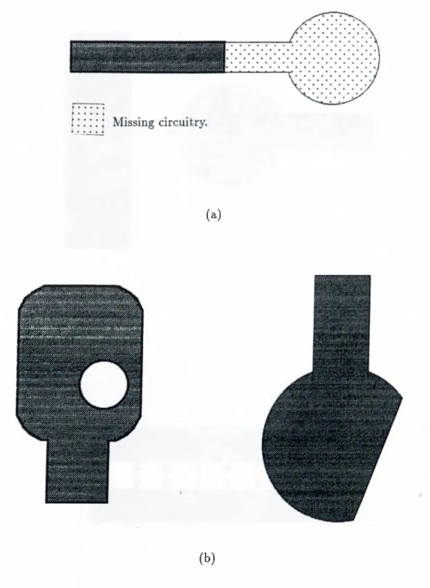
2. Large defects (Non-local defects):
Non-local defects are those whose local properties (those within the order of the nominal conductor trace width) are satisfactory in terms of design rules but whose large scale properties define a generic error. This group of defects can be further classified into the following three categories:
CHAPTER 1. AUTOMATED VISUAL INSPECTION OF PRINTED CIRCUIT BOARDS 11 Si5S‘X‘VA>><S'{s\\NS'Cv.%W.S· '· %·, \ . .«: ,N 555<''55:n'.\<'XnXnnsvNn “Mouse bite” (a) (b)
(c)
(d)
Figure 1.1. Small area defects, (a) intrusion, (b) protrusion, (c) scratch, (d) gouge, (e) splash, (f) pinhole, (g) open circuit, (h) short circuit.
(e)
(f)
(g) (h)
CHAPTER 1. AUTOMATED VISUAL INSPECTION OF PRINTED CIRCUIT BOARDS
13
• missing patterns (circuitry) on the PCB, (Figure 1.2.a), • extra patterns (circuitiy) on the PCB, and
• non-local defects resembling small area defects on a large scale, (Figure 1.2.b).
Since these types of defects do not violate the design rules those are considered in this work, our rule based defect detection algorithms are not capable of detecting and locating these defects.
3. Proximity defects:
Any two conducting structures which come closer together more than the amount suggested by the minimum spacing requirement between conductors, cause a proximity defect. Clearly, these defects violate the minimum spacing requirement between conductors. This type of defects can be further classified into two categories as follows:
• local violation, (Figure 1.3.a), and • sustained violation, (Figure 1.3.b).
The related defect detection algorithm we propose, is capable of detecting and locating both types of these defects.
4. Defects related to the minimum and maximum conductor trace width requirements:
Defects in this group are differentiated from the small area defects in the respect that they have regular edge features and that they extend over PCB areas which cannot be classified as small areas. Clearly, this group of defects can be divided into two subgroups as follows;
• defects related to the minimum conductor trace width requirement, (Figure 1.4.a), and
• defects related to the maximum conductor trace width requirement, (Figure 1.4.b).
5. Acute angle violation defects:
(a)
iN>»^\N»^5kN^s\s-,svN%sv.%^‘i\'v.‘.«ss-;-i*':5x-;'{i>ii<{w:-:»ft':<
>?:-:v:*:v:'v%:;y;’:-ï:*N':v*:’>:4^
^^»^íï^>χtÿ>J^!W»'!^^^>^^S^^><·.^^<V·^V^^%%·ı.^^^^\^VW^«·íîs
(b)
Figure 1.2. Non-local defects, (a) missing circuitry, (b) non-local defects resembling small area defects on a large scale.
CHAPTER i . AUTOMATED VISUAL INSPECTION OF PRINTED CIRCUIT BOARDS 15
(a)
(b)
(a)
r T T T T l f f i i r
(b)
Figure 1.4. Defects related to conductor trace width requirements, (a) violation of minimum trace width requirement, (b) violation of maximum trace width requirement.
CHAPTER 1. AUTOMATED VISUAL INSPECTION OF PRINTED CIRCUIT BOARDS
conductor trace has an interior angle less than a given amount which is typically 70°. In Figure 1.5.a and Figure 1.5.b, two instances of acute angle violation defects are given. Although our defect detection algorithm related to the verification of the minimum spacing requirement between conductor traces is not specifically designed so as to detect acute angle violation defects, it may do so under certain conditions. But, on a general basis, our defect detection algorithms are not capable of detecting defects of this type.
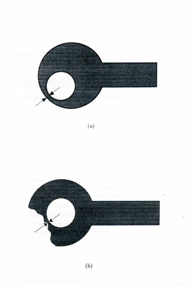
6. Defects related to the misregistration of through holes or vias on lands: Through holes and vias may not be drilled just in the middle of their pads due to some deficiencies in the PCB production process. This results in a misregistration of the through holes and vias in the lands surrounding them. There is a design rule related to such cases, which requires the existence of a minimum land width all around the hole (either a through hole or a via). The cases of hole misregistration, in which this minimum land width requirement is not satisfied, constitute defects. Furthermore, the cases in which the land width is reduced further below this minimum amount due to some other reasons, such as an intrusion on the land, also result in the violation of the above mentioned design rule, and hence, should also be considered as defects. In parts (a) and (b) of Figure 1.6, two instances of the violation of the design rule related to the minimum land width requirement, are shown. In part (a), the violation is due to the misregistration of the hole, whereas in part (b), the violation is due to an intrusion on the land surrounding the hole. Our related defect detecting algorithm, since it directly checks the width of the land, is capable of detecting all defects of this type irrespective of their causes.
(a)
(b)
CHAPTER 1. AUTOMATED VISUAL INSPECTION OF PRINTED CIRCUIT BOARDS 19
(a)
(b)
Figure 1.6. Defects related to the minimum land width requirement, (a) misregistration of the hole, (b) an intrusion on the land.
Mathematical Morphology and Its
Fundamental Definitions
2.1
Introduction
In this chapter, the mathematical background which is necessary for the understanding of mathematical morphology based defect detecting image processing algorithms, will be presented. For this purpose, after a brief introduction about the history and basic features of mathematical morphology given in Section 2.2, some important definitions related to digital topology and the adopted notation conventions will be stated in Section 2.3. In Section 2.4, the fundamental operations of mathematical binary morphology will be defined. Finally, this chapter will be concluded with Section 2.5, in which, two binary morphological algorithms of fundamental importance for the defect detection techniques used in this work are given.
2.2
An Overview of Mathematical Morphology
2.2.1
A Brief History of Mathematical Morphology
Mathematical morphology started in 1964 when Georges Matheron was asked to investigate the relationships between the geometry of porous media and their permeabilities, and when at the same time J. Serra was asked to quantify the petrography of iron ores, in order to predict their milling properties. This initial period (1964-1968) has resulted in a first body of theoretical notions (Hit or Miss transformations, dilations and erosions, boolean models), together with the first prototype of a texture analyzer based on mathematical morphology. It was also the time of the creation of the Centre de Morphologie Mathématique on the campus of the Paris School of Mines at Fontainebleau (France). At the outset, the approach of mathematical morphology was essentially statistical in nature, synthesizing the geometric probability utilized in stei-eology with the shape-oriented Minkowski algebra of Hans Hadwiger.
A more recent branch of mathematical morphology in which we will be mainly interested, is concerned with picture processing. This branch of study appeared in the United States at the beginning of the 1960s as a consequence of the N.A.S.A. activities. This field has gained an ever-growing importance and popularity, and since 1975, the use of the fundamental morphological operations, absent of any significant statistical interpretation, has found a wide field of application in science and technology. Today, its scope has extended to domains other than satellite imagery, its audience has become more international and now is represented by scientific societies such as that of pattern recognition.
2.2.2
Basic Features of Mathematical Morphology
CHAPTER 2. MATHEMATICAL MORPHOLOGY AND ITS FUNDAMENTAL DEFINITIONS 21
From a general scientific perspective, the word morphology refers to the study of form (shape) and structure. The term is used in this sense in biology.
medicine, geography, and linguistics. In image processing, morphology is the name of a specific methodology originated by G. Matheron and J. Serra. The term is appropriate because as it will become more clear soon, morphology based image analysis makes use of the geometric structure inherent within an image.
Mathematical morphology is a branch of mathematics which forms a very natural, pleasing, and unique methodology for image analysis. Its uniqueness arises from the fact that it has a very distinctly flavored theory and set of tools as compared to the other classical methods of image analysis, such as those based on Fourier Transform (Frequency Domain) or convolution (Spatial Domain) techniques. The purpose of mathematical morphology is not only to enhance the images and to recognize their patterns but also to help understand the structures; for example to describe quantitatively the shapes or to explain the concept of “size” . Thus, it provides a means for describing geometrical structures manifested on images. These images, which are either binary or gray level images, are respectively in the form of binary or gray tone functions in two dimensions.
Mathematical morphology provides an approach which is based on shape, for the processing of (digital) images. This, rather interesting methodology of mathematical morphology for image analysis, resulted from the introduction of the concept of structuring elements. Chosen by the morphologist, these structuring elements interact with the (image of the) object under study, modifying its shape and reducing it to a sort of caricature which is more expressive than the actual initial structure of the object. Appropriately used, mathematical morphological operations tend to simplify image data, preserving their essential shape characteristics, and eliminating irrelevances. This feature of mathematical morphology is extensively used in the defect detection algorithms developed in this work.
As the identification of objects, object features, and assembly defects correlate directly with shape, it becomes apparent that for these purposes, i.e. for the purposes of object or defect identification required in industrial
CHAPTER 2. MATHEMATICAL MORPHOLOGY AND ITS FUNDAMENTAL DEFINITIONS 23
vision applications, the operations of mathematical morphology are more useful and powerful than the classical convolution operations employed in signal processing. Thus the natural processing approach to deal with the machine vision recognition process is apparently mathematical morphology since, to mention it once more, the morphological operators relate directly to shape.
2.3
Fundamental Definitions of Digital Topology and
the Adopted Notation
The language of mathematical morphology is that of set theoiy. Sets in mathematical morphology represent the shapes which are manifested on binary or gray tone images. For example, the set of all the black pixels in a black and white image (a binary image) constitutes a complete description of the binary image. Sets in Euclidean 2-space may denote foreground regions in binary images which are usually characterized by black pixels. (Whereas background regions are usually denoted by a set of white pixels.) Sets in Euclidean 3-space may denote time varying binary imagery or static gray scale imagery as well as binary solids. Sets in higher dimensional spaces may incorporate additional image information, like color, or multiple perspective imagery. Mathematical morphological transformations apply to sets of any dimensions, those like in Euclidean N-space (F^"^), or those like in its discrete or digitized equivalent, the set of N-tuples of integers, .
Due to the properties of the underlying problem, we will be mainly interested in the shape analysis of the (foreground) objects present on digital binary images. For this reason and for the sake of being complete and brief, the contents of this section will be kept limited to the related definitions of digital binary image topology, and binary morphology. However, although stated before, it is worth mentioning as a reminder that the methods and the theory of mathematical morphology are by no means limited to digital binary image analysis applications.
2.3.1
Fundamental Definitions of Digital Binary Image
Topology
As stated before, in the following material we will be mainly concerned with set descriptions of digital binary images. For this purpose, on a very general setting, we can consider two-dimensional image arrays as a starting point. Specifically, we will be interested in two-dimensional binary image arrays, all of whose elements have value 0 or 1. The elements of a two-dimensional image array (whether binary or gray-scale) are called pixels. To avoid having to consider the border of the image array we assume at the moment that the array is unbounded in all directions. This final point induces, the previously mentioned set description of a digital binary image as follows. We associate each pixel, regularly, with the corresponding point in the plane Z “ which consists of the ordered two-tuples of integers (x ,y ), x ,y €. Z, where Z denotes the set of integers. More clearly, this regular correspondence between the pixels (the elements of the two-dimensional image array) and the points in the plane Z^ is the trivial one between the pairs of indices of the array elements and the pairs of integer coordinates of the plane points. Hence, we associate the pixel at the row and i^^ column of the two-dimensional image array with the point having the coordinates ( i , j ) in the plane
As a result of this correspondence, we formally define a digital binary image as a set A of points of the plane where A C Z^ (or more generally A C Z^). The elements of Z^ (the points in the plane Z'^) will be called the pixels of the digital binary image (in accordance with the analogy to two-dimensional image arrays). In particular, the points in A with value 1 will be called the foreground pixels or the black pixels of the image; whereas the points in the set Z “^ \ A = all of which have value 0, will be called the background pixels or the white pixels of the image. In the previous statement, the sign \ referred to a set subtraction operation and the set A ‘^ is the complement set of the set A with respect to the (universal) set Z^. We prefer to use the names “foreground pixel” and “background pixel” in order to refer to digital binary image pixels. We also choose to adopt the convention of denoting the
foregi'ound pixels by black points and the background points by white points, unless otherwise stated explicitly. For our case, A will always be a finite set; and in this case the digital binary image is said to be finite.
Two pixels in a digital binary image are said to be 8-adjacent if they are distinct and each coordinate of one differs from the corresponding coordinate of the other by at most 1. More formally, this definition could be stated as follows: Let x = { x i , X2) and y_ = (¿/
1
,7
/2
) be two pixels in a digital binaryimage. Then, x and y_ are said to be 8-adjacent iff (if and only if) the following two conditions are satisfied:
• Х^фух or X2 Ф i/2,
• max[ I - 7/1 I , I :Г
2
-¿/2
I ] < 1 ·Similarly, two pixels in a digital binary image are said to be ^-adjacent if they are 8-adjacent and differ in at most one of their coordinates. More formally, this definition could be stated as follows: Let x_ = ( xi , X2) and y_ = (¿/
1
,^2
) betwo pixels in a digital binary image as before. Then, x and £ are said to be 4-adjacent iff the following two conditions are satisfied:
•
Xi ^ yi ОГХ
2Ф
7/2,• \ x i - y i \ + I
2:2
- 7/2 I < 1·CHAPTER 2. MATHEMATICAL MORPHOLOGY AND ITS FUNDAMENTAL DEFINITIONS 25
In view of the previous two definitions, an 8-neighbor (./-ne/^fièor) of a pixel X, is a pixel that is 8-adjacent (4-adjacent) to x. Clearly, for any pixel in a digital binary image there are 8 distinct 8-neighbors and 4 distinct 4-neighbors. Figures 2.1 and 2.2 show the 8-, and 4-neighbors of a pixel respectively.
A pixel X is said to be 8-adjacent (j-adjacent) to a set of pixels B, if x is 8-adjacent (4-adjacent) to at least one pixel in B. A set of pixels B is said to be 8-adjacent (j-adjacent) to a pixel x, if at least one pixel in B is 8-adjacent (4-adjacent) to x. A set of pixels B is said to be 8-adjacent (j-adjacent) to
•
Center pixel.
8-neighbors of the center pixel.
Figure 2.1. 8-neighbors of a pixel.
•
Center pixel,
4-neighbors of the center pixel.
CHAPTER 2. MATHEMATICAL MORPHOLOGY AND ITS FUNDAMENTAL DEFINITIONS 27
another set of pixels C, if at least one pixel in B is 8-adjacent (4-adjacent) to at least one pixel in C.
We say a set B of pixels in a digital binary image is 8-connected (4- connected) if B cannot be partitioned into two subsets that are not 8-adjacent (4-adjacent) to each other. An 8-component (4-component) of a set of pixels B is a non-empty 8-connected (4-connected) subset of B which is not 8-adjacent (4-adjacent) to any other pixel in B.
Two foreground pixels in a digital binary image are said to be adjacent if they are 8-adjacent, and two background pixels or a background pixel and a foreground pixel are said to be adjacent if they are 4-adjacent. The reason for using different kinds of adjacency for the foreground and background pixels, is to avoid some parado.xes related to the adjacency and connectivity properties on digital binary images. (Two of such paradoxes are given in [20].) Hence, we assume that, the set A which describes the digital binary image and consists of all of the foreground pixels of the image is composed of a finite number of 8-components, whereas the set which consists of all of the background pixels of the image is composed of a finite number of 4-components, with a unique infinite 4-component of background pixels. However, in the following material, for the sake of simplicity we Avill assume that the set A ‘^ is also a finite set, large enough to cover the foreground pixels in a rectangular region of background pixels.
The 8-neighborhood (4-neighborhood) of a pixel is a set containing the pixel and its 8-neighbors (4-neighbors).
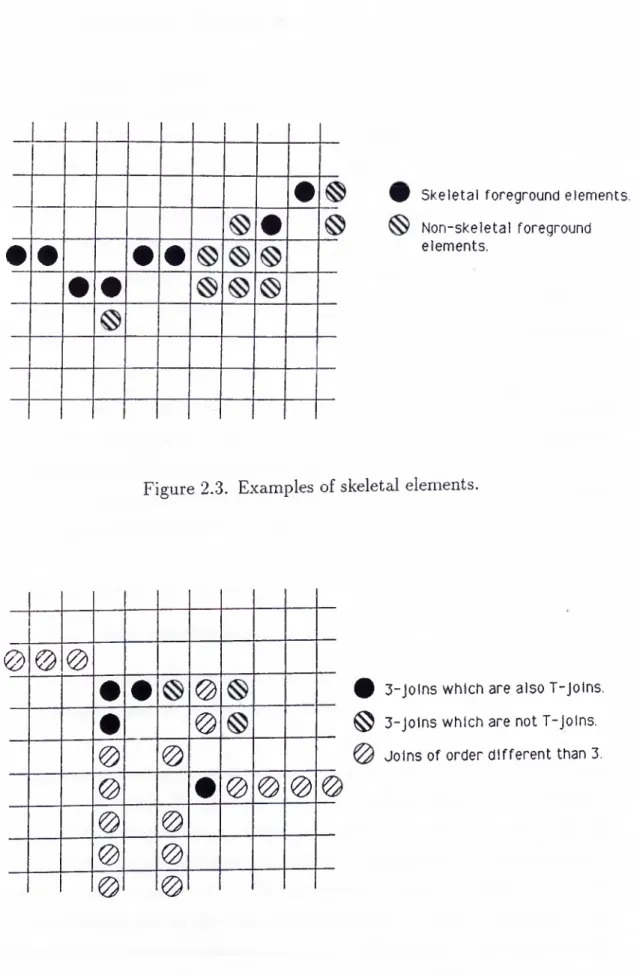
A skeletal element is a foreground pixel that is necessary to maintain the 8-connectivity of its 8-neighborhood; i.e. changing the pixel to a background pixel breaks the 8-connectivity between at least two other foreground pixels in the 8-neighborhood. Some examples of skeletal and non-skeletal elements are given in Figure 2.3. An n-join is a foreground pixel with n foreground 8-neighbors; hence, a join can be of order 0 to 8. A T-join is a 3-join whose 8-neighborhood contains only skeletal elements. Some examples of T-joins are given in Figure 2.4.
i
•
#
# •
• #
#
•
9 Skeletal foreground elements. Non-skeletal foreground elements.
Figure 2.3. Examples of skeletal elements.
©
0
©
# •
0
•
©
©
©
©
# © © © €
0
©
©
©
0
©
9 3-Jolns which are also T-Jolns. ^ 3-Jo1ns which are not T-Jolns.
Joins of order different than 3.
CHAPTER 2. MATHEMATICAL MORPHOLOGY AND ITS FUNDAMENTAL DEFINITIONS 29
2
,
3 , 2Adopted Notation
Before stating the definitions of the three fundamental binary morphological operations of Hit or Miss transformation, dilation, and erosion, for the sake of clarity it will be wise to introduce the adopted notation, and use these conventions all throughout the following material.
Morphological operations are defined between two sets. In practice, these two sets are handled quite differently. The first operand (set A) is considered as the image undergoing analysis, while the second operand (set B ) is referred to as the structuring element, to be thought of as constituting a single shape parameter for the specific morphological transformation under consideration.
Thus, consistent with our previous notation, in the following material the set A will refer to the image which is a digital binary image defined through the set (/1) of all of its (black) foreground pixels residing on the (white) bcickground. Also consistent with the previously mentioned convention, the set B will refer to the structuring element. The structuring element in the most general case contains three different kinds of pi.xels which can be classified as follows:
1. pixels which should belong to the foreground,
2. pixels which should belong to the background,
3. pixels which are don’t care pixels and thus which may belong either t o ' the foreground or to the background.
The resultant set of the morphological operation defined on A and B will be denoted by the letter X . This set X is the resultant digital binary image of the morphological operation. Clearly, all of these three sets, namely A, B, and X are subsets of the digitized or discrete equivalent of the two-dimensional Euclidean space, namely Z^. The elements of these sets which are called pixels and which are in fact points in the plane Z'^ will be denoted by the corresponding underlined lower case letters. The notation of the pixels with underlined small case letters stresses on the 2-dimensional vector interpretation
of the points in the plane (or equivalently of the pixels in a digital binary image) which will be quite useful in the following definitions. Hence, we have a E A, b € B, and ^ £ X . In general, it will prove to be quite useful to specifically denote the center point of the plane Z^, namely the point (0,0). This will help to explicitly fix the pixels of an image or a structuring element. Unless otherwise stated, we will adopt the convention that the center pixel of a structuring element is coincident with the center point of the plane Z^. Wherever necessary, the center point of the plane Z^ will be denoted by a point from which two little arrows in the conventional x-axis and y-axis directions, emerge.
2.4
Basic Morphological Operations and Some Related
Fundamental Propositions
In the following subsection, after the statement of some preliminary definitions, the three fundamental operations of mathematical morphology namely the Hit or Miss Transformation, the Dilation operation, and the Erosion operation will be introduced.
2.4.1
Basic Morphological Operations
The first notion we need in the following definitions, is the vector addition of two points in the plane Z “^. Although quite trivial, the definition of this operation will be restated here for the sake of being complete.
For every w = (wi,W2) and y_ = ( yi , y2) belonging to Z^, we define the
(vector) addition of w and £ as follows:
w +
2
/ = (wi + yuW2 +2
/2
)·One of the other notions which we will need is the translate of a set in Z “^. This operation can be defined as follows: Let H be a subset of Z"^ and let y_ be
CHAPTER 2. MATHEMATICAL MORPHOLOGY AND ITS FUNDAMENTAL DEFINITIONS
31
an element of . Then the translate (translation) of the set B by the point (or equivalently the vector) y, is denoted by By and is equal to,
-By = .Y = I X = y + 6, 36 € B } .
Clearly, this definition is the discrete equivalent of the familiar linear translation operation in E^.
Now, the definition of the Hit or Miss Transformation which represents the hearth of many morphological operations, can be stated.
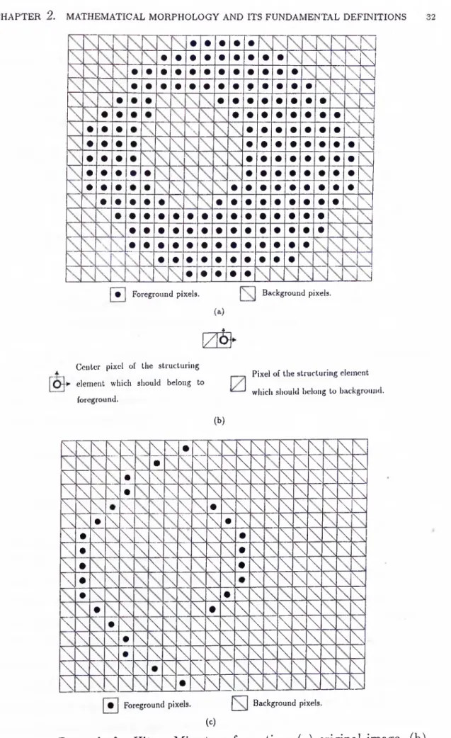
H it or M iss T ra n sform a tion . The Hit or Miss transformation is basically a template matching process. Let A denote a set in Z^, representing the foreground pi.xels in a digital binary image. Then (the complement set of the set A) represents the background pixels. Let B be another set in the same plane, representing the chosen structuring element. Let B^ and be two sets such that B^ C B, B^ C B, and .B^ U B^ = B, (i.e. B is composed of the two subsets B^ and B^). Then the Hit or Miss transformation of the set A by the set B (with respect to the given decomposition of B). is denoted by A 0 B and is defined as the set of all points ^ where Bl is included in A and B j is included in A ‘^. Equivalently,
A 0 B = X = {x\ B l c A and B l c A^}.
Clearly, a necessary condition for A 0 B being non-empty is that B^ fl B^ = 0.
An example of the Hit or Miss transformation is given in Figure 2.5. In part (a) of this figure, a typical digital binary image of a via on a PCB is given. Our aim is to find the total number of the horizontal foreground line segments present in this image. For this purpose, we use the structuring element shown in part (b) of the same figure. Note that, this structuring element will score a hit on the image only at the places where a cross sign is formed on the left pixel of the structuring element, and also the annular region on the right pixel of the structuring element is filled so as to form a solid circle. Clearly, this situation will occur only at the starting point of each horizontal foreground line segment. The resultant image of the Hit or Miss transformation of the
\ V \ \
N
_\ \ \ \I # [ Foreground pixels. Background pixels.
(a)
0 ^
Center pixel of the structuring element which should belong to foreground.
Pixel of the structuring element wliicli sliould belong to background.
(b)
\\\ \ \\\•k \kkkkk k
\ • ,\kkk kkkk k
\ \ •\\\
k\k\kkkkk\
\\\\\• \\\k\k\kkkkkkkk
\\\ \ \\\#kkkkkk kkk
\ •N\\ \kk•k kkkk k\
\•\ \\,\ \\k•k \kkkkk
\•\ \\\\ \\jk#kk k kkk
\
k
\kk kk•kkk k
0 \\\ \k k kkkkkk k
•\
k\•\kk kkkkjk
• \ \ \#kkk k k k
\\ •\ \ \\kkkkkkk\k
\\\•\ \ \\kk kkkk kk
\\ \•\\ \\\ \k kkkk k
\\\ \\ \ kkk \k kkk k
\
•\k
[ # I Foreground pixels. Background pixels.
(c)
Figure 2.5. Example for Hit or Miss transformation, (a) original image, (b) the structuring element to be used, (c) result of the transformation.
original image in part (a) with the structuring element in part (b), is given in part (c). The number of the foreground pixels in this final image (25), is equal to the number of the horizontal foreground line segments present in the original image.
E rosion O p era tion . If is the empty set, then the condition C
in the definition of the Hit or Miss transformation is always satisfied. This particular case of the Hit or Miss transformation is known as the erosion of the set A by the structuring element B and is denoted by A G 5 . Equivalently, since B^ = 0, we have B^ = B and,
A Q B = X = {x \B,<z A] .
Thus, the erosion of an image A by a structuring element B is the set of all points X of Z~ for which B translated to x is contained in A.
At this point, it is proper to state an equivalent definition of the erosion operation, which will be useful for the construction of a proof of a duality relation between the erosion and dilation operations. This duality relation will be given in Subsection 2.4.2.
P ro p o s itio n 1:
A Q B — C\bsB-^-b · A proof of this proposition is given in [23].
Erosion shrinks (tapers) components. By this, it is meant that if the erosion operation is carried far enough, i.e. repeatedly applied a sufficient number of times with a suitable structuring element, components may break up or disappear completely. Thus, erosion operation may destroy the connectivity properties of a digital binary image. This feature of the erosion operation is rather important and is in fact extensively used in our defect detection algorithms. An example of the erosion operation is given in Figure 2.6. In part (a) of this figure, a typical digital binary image captured from a PCB is given. This image contains a conductor trace ending in a via. In part (c) of the same figure, the image obtained after the erosion of the original image for one time
· · · · · · · · · · · · · · · · · · · · · · · · · · · · · · · · · · · · · · · · · · · · · · · · · · · · · · · · · · · · · · · · · · · · · · · · · · · · · • · · · · · · · · · · · · · · Foreground pixels. (a)
•
•
• i ·
•
•
•
(b) · · · ' ■ * · · ' * • · · · ■ . · · ...· · · · · · · · · # · · ^ · * • · · · · · · ·Foreground pixels removed after erosion.
Foreground pixels remaining after erosion.
(c)
Figure 2.6. Example for erosion operation, (a) original image, (b) the structuring element to be used, (c) the result of the erosion operation.
with the structuring element given in part (b), is shown. Notice the changes in the connectivity properties of the image.
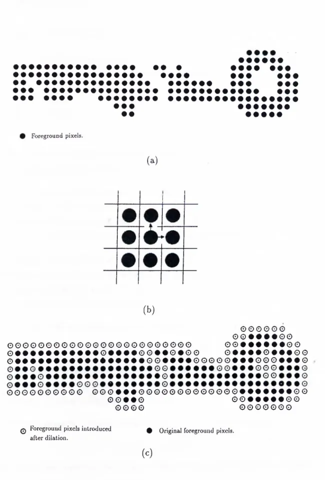
D ila tio n O p era tion . Dilation is the morphological transformation which combines two sets using the vector addition of set elements. Let A and B be two sets in as before. Then the dilation of the set A by the structuring element B is denoted by A © 5 and is defined as the set of all possible vector sums of pairs of elements, one element coming from A and the other one coming from B. Equivalently,
A ® 5 = X = { s | x = a + 6, 3a€ A, 3 6 G
B}.
The following two properties of the dilation operation, the proofs of which are omitted since they are very straight forward, will be useful in our future work. However, the interested reader can find the proofs of these two propositions in [23].
P ro p o s itio n 2: The dilation operation is commutative; i.e.,
A ® B B ® A.
P ro p o s itio n 3: The dilation operation is associative; i.e.,
A ® {B ® C) = [A ® B ) ® C.
CHAPTER 2. MATHEMATICyVL MORPHOLOGY AND ITS FUNDAMENTAL DEFLNITIONS 35
At this point, it is proper to state an equivalent definition of the dilation operation, which will be useful for the construction of a proof of a duality relation between the erosion and dilation operations. As mentioned before, this duality relation will be given in Subsection 2.4.2.
P ro p o s itio n 4:
A ® B
U6gBAfc.
A proof of this proposition is given in [23].Dilation expands components and fills in details. By this, it is meant that if the dilation operation is carried far enough, i.e. repeatedly applied
a sufficient number of times with a suitable structuring element, components may merge together, and holes may become filled and thus disappear. Thus, dilation operation may destroy the connectivity properties of a digital binary image. This feature of the dilation operation is rather important and is in fact extensively used in our defect detection algorithms. An example of the dilation operation is given in Figure 2.7. In part (a) of this figure, a typical digital binary image captured from a PCB is given. This image contains a conductor trace ending in a via. In part (c) of the same figure, the image obtained after the dilation of the original image for one time with the structuring element given in part (b), is shown. Notice the changes in the connectivity properties of the image.
In the following subsection, three important properties of the morphological operations will be stated. These properties have great practical significance related to the implementation of morphological operations on image processing hardware.
2.4.2
Three Important Properties of Morphological
Operations
Proposition 5: Decomposition of the dilation structuring element ( “Chain
rule” for dilations).
A
0(Bi
0 J?2 0 ··· 0B
n)
= ((•••((^ ® -^i) ®B
2)
0 ...) 0B
n)·
The proof of this equality immediately follows by the iterative use of the associative property of the dilation operation on the left hand side of the above equation.
This relation is very important since it implies that a large dilation can be computed by N successive smaller dilations if the structuring element used for dilation can be decomposed into the dilation of N smaller structuring elements.