Low temperature grown GaAs based resonant cavity enhanced photodiodes
Tam metin
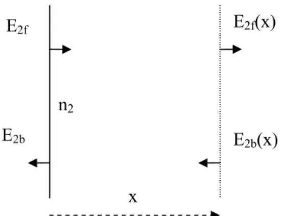
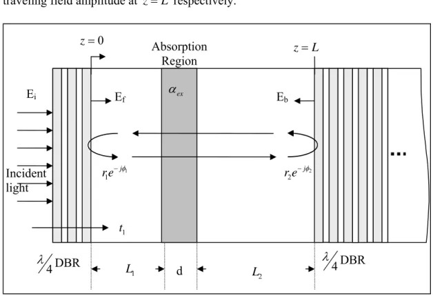
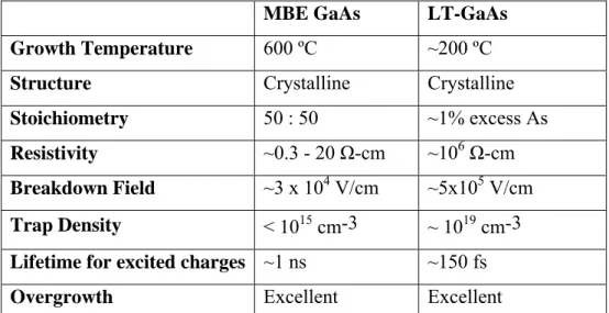
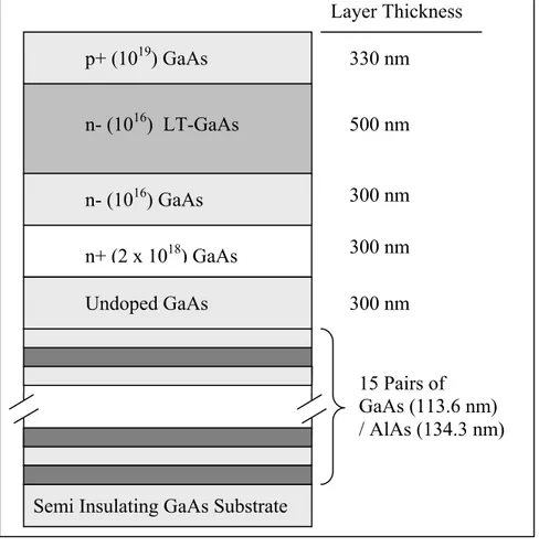
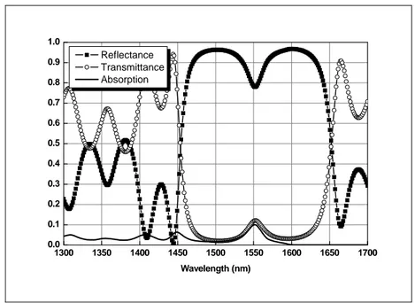
Şekil
![Table 2.2: Absorption lengths of GaAs and LT-GaAs at different wavelengths, where detectors were fabricated [3]](https://thumb-eu.123doks.com/thumbv2/9libnet/5866479.120718/38.892.207.767.381.505/table-absorption-lengths-gaas-different-wavelengths-detectors-fabricated.webp)
Benzer Belgeler
After briefly introducing each party under examination in their respective sub-sections, their conceptions of “the international” as found in their party programs and
this model disclosed that intrinsic attitude towards science (AS) (career preference, emotional states towards science and favourableness towards school science) has positive
In prescribing how best to proceed from here, two main points must be made at the outset. First, there is the need to reiterate that a successful roadmap to deal with the
composite NFs; HAADF-STEM and STEM EDAX mapping images of ZT-SN 00 NFs; XRD spectrum of ZT-SN 200 NF; EDAX spectra of ZT-SN based NFs; TEM and STEM-EDAX mapping images of ZT-SN 150
1) a valid, signed contract with a customer: According to Paragraph 17 of SOP 97-2, revenue should not be recognized unless persuasive evidence of an arrangement exists even if
intermixing suppression, we demonstrate an IFVD process for high power semiconductor lasers with good surface morphology, large QWI selectivity, high quantum ef ficiency and
Conservative occlusion culling for urban visualization using a slice-wise data structure.. Tu¨rker Yılmaz, Ugˇur
To avoid the misuse of SMCs, some principles should be accepted and regulated such as separation of assets, the doctrine of piercing the corporate veil, prohibition on loans to
