Contents lists available atScienceDirect
Precision Engineering
journal homepage:www.elsevier.com/locate/precision
Polycrystalline diamond end mill cutting edge design to improve
ductile-mode machining of silicon
S.N.B. Oliaei
a, Y. Karpat
b,c,d,⁎aAtilim University, Department of Mechanical Engineering, Incek, Ankara, Turkey bBilkent University, Department of Industrial Engineering, Bilkent, Ankara, Turkey cBilkent University, Department of Mechanical Engineering, Bilkent, Ankara, Turkey
dUNAM-National Nanotechnology Research Center and Institute of Materials Science and Nanotechnology, Bilkent University, Ankara, Turkey
A R T I C L E I N F O
Keywords: Micro milling Single crystal silicon Ductile mode machining Polycrystalline diamond
A B S T R A C T
Silicon is a commonly used material in optoelectronics and microfluidics devices. Micro mechanical milling of silicon with polycrystalline diamond (PCD) tools has the potential to produce three-dimensional surfaces with good surfacefinish and an increased material removal rate. PCD micro end mill geometry is known to influence process outputs yet its effect has not been studied in detail. In this study, a PCD end mill with a hexagonal geometry has been considered, and its micro cutting geometry has been modified to have a parallelogram shape featuring a large negative rake angle on the bottom of the tool. The proposed micro geometry also reduces the contact area between the tool and the work material. The proposed geometry was fabricated using wire electric discharge machining (WEDM). Ductile-to-brittle transition conditions and areal surface roughness have been investigated as a function of tool geometry and feed during micro milling of silicon. A significant improvement in material removal rate and surface roughness has been obtained compared to a commercially available PCD end mill having hexagonal geometry withflat bottom. The results show that PCD micro end mill geometry sig-nificantly affects the process outputs.
1. Introduction
Due to rapid growth in the electronics, optics, and biomedical in-dustries, there is an increasing demand for components made from semiconductor materials such as silicon. While lithography and etching techniques are used to process silicon, they are typically limited to planar surfaces. Micro mechanical milling is considered a flexible technique that is capable of machining three-dimensional complex features on silicon. Polycrystalline diamond (PCD) is a cutting tool material suitable for silicon machining, and one that can be fabricated to have a complex geometry using wire electric discharge machining (WEDM). The literature contains only a limited number of studies considering the influence of PCD tool geometry on process outputs. The aim of this study is to improve the micro geometry of PCD end mills.
Silicon is known to be difficult-to-machine due to its high hardness and low fracture toughness. Excessive surface and subsurface damage may occur if machining conditions are not carefully selected. In order to obtain ductile mode machining, certain conditions at the cutting zone must be satisfied so that brittle fractures are suppressed during machining. Blake and Scattergood [1]defined the term critical chip thickness, which in-dicates the transition from ductile to brittle chip formation during single
point diamond turning of silicon. The feed must be selected such that cracks do not reach the machined surface. Nakasuji et al.[2]proposed a model for brittle to ductile transition by considering slip and cleavage mechanisms during chip removal. Ductile behavior of brittle materials has been related to high pressure phase transformation under which the semiconducting material goes through a metallization process and starts acting like a ductile material[3]. Therefore, the use of large negative rake angles and round cutting edges are required to obtain high hydrostatic pressures at the cutting zone for ductile chip formation, which directly affects the surface quality. Yan et al.[4]investigated the subsurface da-mage while machining silicon and observed that the length of subsurface damage can be significantly larger than the depth of cut. Molecular dy-namics simulations have been used to investigate issues like subsurface damage while machining of brittle materials[5,6]. Process parameters such as depth of cut and feed rate must be selected carefully based on the cutting tool geometry, which is defined using rake angle, clearance angle, and cutting edge radius. In diamond turning of brittle materials, tools with large negative rake angles (between−20° and −45° degrees) are used to obtain such conditions at the cutting zone. Hu and Melkote [7] in-vestigated the ductile-to-brittle transition during diamond scribing of si-licon. A extensive review of silicon machining is given in[8].
⁎Corresponding author at: Bilkent University, Department of Industrial Engineering, Turkey.
E-mail address:[email protected](Y. Karpat).
Precision Engineering 51 (2018) 403–414
The number of studies on micro milling of silicon is limited
com-is possible with ball end mills. Arif et al.[11]developed an analytical model and showed that if the radial depth of cut is larger than the length of the subsurface damage, ductile mode machining in brittle materials is possible. Golshan et al.[12]used CBN micro end mills to Fig. 1. Ductile-to-brittle transition during incline plunge micro milling process.
Fig. 2. a) 3D CAD model of the novel PCD micro end mill design, b) Detailed description of the tool geometry with its parameters.
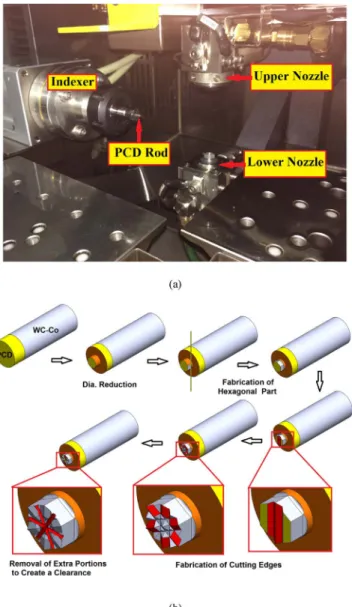
Fig. 3. (a) Wire EDM setup, (b) Fabrication process steps of PCD micro end mill.
Table 1
WEDM process conditions to fabricate PCD tools.
Roughing Finishing
Pulse On Time (μs) 2.5 2.5
Pulse Off Time (μs) 5 7.5
Reference Voltage (V) 170 120
Supply Voltage (V) 5 2
Peak Current (A) 3.6 0.6
Capacitance (nF) 200 200
Wire Speed (m/min) 3 5
Inverter Frequency (Hz) 20 12
machining based on the crystallographic orientation of the material. Huo et al.[14]studied the surface and subsurface characterization of slot micro milled silicon with (100) orientation using CBN and diamond coated carbide end mills of 0.5 mm diameter. The results indicated the importance of feed selection where low feeds are necessary to obtain ductile mode machining. Cheng et al. [15] developed a generalized model for micro milling of silicon based on indentation tests. They
concluded the importance of cutting edge radius on ductile mode ma-chining.
In the literature, micro cutting tools made from polycrystalline diamond (PCD) have been shown to work effectively to machine brittle materials such as glass, silicon, silicon carbide and tungsten carbide [16–19]. Wire electric discharge machining (WEDM) technique is usually employed to fabricate PCD micro tools. Cheng et al. [20] Fig. 4. Material removal mechanisms of PCD during a) rough EDMing, b) finish EDMing, c) Surface quality of resulting PCD surface.
designed an ultra precision machine tool which is capable of fabricating complex tool geometries. A two-flute and a hexagonal shaped PCD micro end mill were produced with the system and successfully ma-chined brittle materials. The surface quality of the PCD tool and the cutting edge radius are important factors which are related to the WEDM process parameters. Cheng et al.[21]performed an analysis of micro tool geometries presented in the literature and laid down a guideline for an effective micro tool design. They indicated the im-portance of rake angle, cutting edge radius, the amount of contact be-tween the tool and the workpiece both on the periphery and on the tool bottom. Zhongbo et al.[22]also developed a methodology for PCD end micro end mill design. Recently, Oliaei and Karpat[23]fabricated PCD micro end mills for machining silicon.
This study considers micro milling of silicon with the focus on tool micro geometry. The goal of this study is to understand the interplay between tool geometry and process outputs by using a systematic ap-proach. Areal surface roughness and critical depth of cut are used to study the effect of tool geometry together with process parameters. A novel PCD tool geometry is proposed and successfully fabricated to machine silicon. The performance of the proposed tool geometry is compared with the commercially available hexagonal PCD end mill which has been employed in silicon machining studies in the literature [19].
2. Ductile mode machining of silicon
Ductile mode machining of brittle materials requires careful selec-tion of feed and depth of cut values. Geometric, thermal, static, dy-namic, and kinematic behaviors of the machine tool are also known to
influence the surface quality. Blake and Scattergood[1]put forward an important concept in ductile mode machining based on the critical chip thickness during diamond turning. Depending on the selection of feed, cracks form along the cutting edge. If the chosen uncut chip thickness is less than the critical chip thickness value, cracks formed along the cutting edge do not reach the surface and are machined away in the next cut, thereby obtaining a crack-free surface. If a large uncut chip thickness is set, the length of the cracks is larger and they appear as a crack on the machined surface. Cracks on the surface affect the surface integrity of the machined part.Fig. 1shows the similar relationship between depth of cut and ductile-to-brittle transition for incline plunge cut during micro milling. As depth of cut increases, the size of the fractures at the cutting zone increases and reaches to a length which is larger than the actual depth of cut and hence appear on the machined surface as pits which decrease the surface quality.
In order to obtain a crack-free surface, it is important to control the compressive and tensile stress regions under the cutting edge. It is important for cutting geometry to create ideal conditions for ductile chip formation which will yield superior surface quality. High pressure phase transformation (HPPT) where semi conductor material acts like a metal under high hydrostatic stresses is responsible for ductile behavior of the material[3–6]. Tool micro geometry has an important role in obtaining high hydrostatic pressure at the cutting zone. While ma-chining with single crystal diamond tools, which have edge radius in the order of tens of nanometers, large negative rake angles (around −25° to −45°) are usually used[24]. Cutting edge radius is known to act like a negative rake angle when uncut chip thickness is set to be less than the edge radius of the tool[25]. Clearance angle is also important to reduce the rubbing on the cutting edge during machining. Yan et al. Fig. 5. a) 3D profile of the fabricated PCD tools, b) PCD cutting edge obtained at low discharge energies.
[4]conducted plunge cutting tests performed on silicon along various directions and observed the importance of crystallographic effects on subsurface damage. They recommended large negative rake angle and small depth of cuts to reduce microcracks. They also identified four kinds of material responses such as amorphization, polycrystallization, microcracking, and dislocation formation. Zhao et al.[26]performed nano indentation tests on silicon and concluded that during nano scale machining the material undergoes phase transformation. The hardness of the machining induced subsurface was found to be softer than the material, which affects the processing of the material.
3. Proposed PCD micro end mill geometry
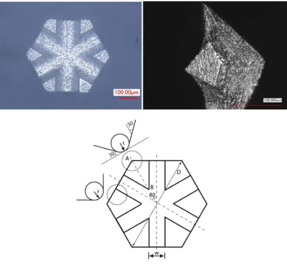
Based on the information given in the previous section, the in flu-ence of rake angle, clearance angle, and the cutting edge radius must be considered in micro geometry design.Fig. 2a shows the CAD model of the proposed geometry. It has a hexagonal form and the geometry of the teeth has been designed to have a parallelogram shape, which possesses a large negative rake angle and a large clearance angle.Fig. 2b defines the necessary geometrical parameters. The micro end mill geometry is mainly defined by its diameter (D), number of cutting edges (n), and the distance between edges (w). The hexagonal end mill (n = 6) has a negative rake angle of−30° and a clearance angle of 30° on the outer edge. The number of edges affects the negative rake angle. Cutting edge radius (r) depends on the process used to fabricate the micro end mills and grain size of the PCD. The length of the edges (L) is also a function of the number of edges (n) and the distance between edges (w). In-creasing the distance between cutting edges (w) decreases the length of the cutting edge. The bottom surface geometry of the tool is also de-fined by a negative rake angle (α) and clearance angle (γ). This sec-ondary cutting edge (AB) at the bottom of the surface has been in-troduced to increase hydrostatic pressure on the surface and to minimize the contact area between the tool and the work material during machining. A line contact between the tool and the work ma-terial minimizes the rubbing action between the mama-terial and the tool. The selection of tool geometry parameters are constrained by the strength of the cutting edge and the stiffness of the tool. When brittle materials such as silicon are machined, it is important to remove the material debris in front of the tool to improve the surface quality. In-novative ideas to prevent this issue have been proposed by integrating electrochemical cleaning techniques into the micro milling process to prolong tool life while maintaining high surface quality[17–19]. Heavy use of lubricants is recommended during machining of brittle materials to help remove machining debris from the cutting zone.
Considering brittle nature of silicon, low feed per tooth and depth of cut values are used in silicon machining practice. As a result, the cutting edge radius is usually larger than the feed per tooth value; therefore, the effective rake angle may become even more negative. As mentioned above, a large negative rake angle is required to increase the hydro-static pressure in front of the tool to obtain ductile mode machining. 3.1. Fabrication of PCD micro end mills
In this study, micro end mills have been fabricated using WEDM process. A Sodick AP250L high precision WEDM machine was used to fabricate PCD tools with diameters of 450–500 μm. PCD tips which are brazed onto WC substrates are mounted on the indexing spindle of the WEDM machine as depicted inFig. 3a. During experiments, the con-centricity between the tool and rotational axis of the indexer is closely controlled. WEDM of the PCD is conducted by using 30μm tungsten Fig. 6. (a) Micro milling experimental setup, b) Crystal directions of (100) Si sample.
Table 2
Material properties of silicon used in this study.
Hardness (Vickers) 1300
Modulus of Elasticity (GPa) 180
Stiffness (mN/nm) 1.2
(TWS-30, 3330 N/mm2 tensile strength) wire diameter. Oil is used (EDMfluid 108 MP-S) as a dielectric fluid.Fig. 3b shows the wire EDM processing steps to obtain the proposed geometry. First, the hexagonal tool shape is obtained by rotating the round tool around its axis and applying wire EDM cuts along its longitudinal axis. In the next step, V-shaped slots are machined on the hexagonal geometry to create the parallelogram shape on each corner of the tool. In three consecutive steps, thefinal micro geometry has been obtained. The length of the edges (L) is 70μm, and the distance between edges (w) is 75 μm.
Yan et al.[27]studied the mechanism of material removal on PCD during EDM process. They showed that maintaining low energy dis-charges effectively decreases the material removal rate of cobalt binder and graphitization of diamond grains. Table 1shows the wire EDM parameters used in PCD tool fabrication. At high energy discharges, the dominant material removal mechanism of PCD is believed to be the melting of cobalt binder and dislodgment of diamond grains [27]. When using wires as small as 30μm, WEDM energy level should be kept very low to avoid wire breakage and to obtain a low surface roughness on PCD. At low discharge energies, gradual removal of diamond grains occurs as a result of graphitization.Fig. 4a and b explain the material removal mechanism during EDMing of PCD [27].Fig. 4c shows the photograph and the topography of the surface obtained after the
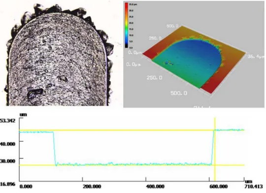
finishing pass, where a surface roughness of 0.11 μm was obtained. Fig. 5a shows the 3D topography of the fabricated tool, where a laser scanning microscope (Keyence VK-X100) measured the cutting edge radii of the tools to be around 1.8μm as shown inFig. 5b. The negative rake angle was obtained as−45°.
3.2. Experimental setup for micromilling
Micro-milling experiments were carried out in a micro machining centre (Mikrotools DT 110). A high speed brushless electric spindle (Nakanishi E3000 with max 50.000 rpm) was integrated into the system and rotational speed was kept at 45000 rpm in order to obtain an accep-table feed rate in experiments. The spindle has a runout of less than 1μm. Experiments were performed on aflat silicon window having 50 mm diameter and 3 mm thickness. Silicon crystal (p–type, doped with boron) has (100) surface orientation. Its directions with respect to X and Y axis of the machine are shown inFig. 6a.Fig. 6b shows the possible pitting da-mage zones for (100) orientation which presents itself in simple four-fold symmetry (shown as gray regions in thefigure). The fracture toughness of the material is known to be lower in those regions[28]. The micro ma-chining experiments were performed in [010], [100], [[0 1 0]], and [[ 1 0 0]] directions. In order to identify silicon material properties, Fig. 7. Hexagonal PCD (commercial) micro end mill design and its parameters.
nanoindentation (Anton Paar NHT3, Oliver & Pharr method with Berko-vich tip) and micro Vickers hardness tests (Zwick) were conducted. Table 2summarizes the identified material properties.
Micro machining experiments were performed to investigate the ductile-to-brittle transition and areal surface roughness of the machined surface. Silicon work material is slightly tilted to observe the influence of increasing depth of cut for a given feed and rotation speed. Odorless mineral spirits (OMS) was used as coolant during experiments. Machining zone was flooded with OMS during experiments.
Topographies of the machined surface and the tools were obtained using a laser scanning microscope (Keyence VK-X100).
In order to evaluate the performance of the proposed design, a commercially available PCD tool (NS Tools, PCDSE 0.5 mm diameter) with hexagonal geometry was also included in the experiments. The commercial tool has aflat bottom surface, which yields a zero degree clearance angle acting like aflank edge.Fig. 7shows the geometry of this tool. It can be seen that the large negative rake angle can be ob-tained due to edge radius which is also measured to be around 2μm. Fig. 8. a) Surface profiles of the machined channels, b) Influence of feed on areal surface roughness (Sa) and critical depth of cut during ductile mode ma-chining using proposed PCD tool design.
There is no difference in the PCD material properties between the commercial and self fabricated tools since the proposed geometry was fabricated after the tips of the commercial tools were cutoff with EDM. 4. Comparing PCD micro end mill performances
The micro milling characteristics of PCD micro end mills were in-vestigated by considering surface roughness and critical depth of cut
where transition from ductile mode machining to brittle mode starts. The influence of feed rate on the surface roughness and critical depth of cut was investigated where feed per tooth values were set as 0.025, 0.05, and 0.1μm/tooth. The areal surface roughness (Sa) was measured as process output. According toFig. 8, as expected, surface roughness increases with increasing feed. Ductile-to-brittle transition depth de-creases with increasing feed. There is a significant increase in surface roughness after 0.05μm/rev feed value.
Fig. 9. Influence of feed on critical depth of cut using commercial PCD tool design a) Machined channels, b) Variation of surface roughness and critical depth of cut as function of feed.
Fig. 9shows the influence of feed on critical depth of cut and surface roughness for the commercial PCD tool. Similarly, as feed increases, the critical depth of cut decreases. The surface roughness seems to be im-proving with increasing feed, but after 0.05μm feed it significantly increases. For both PCD tools, cracks on the machined surface started
before any fractures appeared on the side walls of the slots. Feed value of 0.05μm/tooth and depth of cut around 0.5 μm for ductile mode machining is in agreement with the process parameters recommended by the tool manufacturer. The proposed design allowed for a nearly fourfold increase in critical depth of cut with the surface roughness (Sa) Fig. 10. Influence of increasing depth of cut on the machined channel with proposed tool design.
Fig. 11. Influence of increasing depth of cut on the machined surface with commercial PCD tool (feed per tooth is 0.025μm/tooth).
value of 100 nm compared to a commercial PCD tool.
Fig. 10shows the machined channels at the feed value of 0.05μm/ tooth with the proposed design. When depth of cut reaches to 4μm, some fractures start to appear on the machined surface, and as it reaches 5.5μm significant numbers of fractures occur on the machined surface. An increasing number of elliptical pits on the surface sig-nificantly deteriorate the surface quality.
Fig. 11shows the results when the commercial PCD tool was tested under the same conditions. A significant difference was observed where the transition from ductile to brittle region is observed to be around 1μm. When the depth of cut reaches 4.5 μm, the percentage of pits on the surface increases significantly.Fig. 12shows the surface where the depth of cut is increased to 20μm. Larger fractures on the side walls start to appear. Larger fractures are machined away as the tool ad-vances in the direction of the cut.
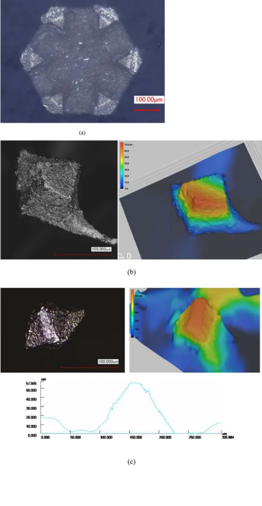
The results imply that a large negative rake angle at the outer dia-meter of the hexagonal tool geometry is capable of suppressing frac-tures at that zone. Not having a negative rake angle and aflat surface on the bottom surface hinders the quality of the machined surfaces and limits the critical depth of cut to lower values. Fig. 13a shows the bottom surface of the commercial tool after machining experiments. Adhered silicon on the cutting edges at large depth of cut tests can be seen. After cleaning the tool using an ultrasonic cleaner, rounding of the cutting edge (Fig. 13b) which limits the ability of ductile mode ma-chining can be observed. After edge rounding, material adhering ac-celerates, which hinders the surface quality. Such problems can be circumvented or minimized by heavy coolant usage at low depth of cut machining cases.Fig. 13c shows the worn cutting edge of the proposed end mill. As expected,flattening of the cutting edge can be observed. The contact area is still smaller than the commercial tool.
Fig. 14a shows the surface topography with proposed geometry
corresponding to 1μm depth of cut (ductile mode machining case) at 0.05μm/tooth feed value. The surface roughness (Sa) is measured as 17 nm, which can be considered an optical surface quality.Fig. 14b shows the variation of surface roughness as a function of feed. At ductile mode, the influence of feed is observed to be low, although feed is increased significantly.
It must be noted that the proposed PCD tool has a more complex geometry compared to the commercial PCD tool. When the cost of al-ready expensive PCD tools is considered, increasing the complexity of the tool design may further increase it. However, a significant increase in material removal rate as shown in experiments may decrease the total machining time and hence justifies the increased cost of the tools. 5. Conclusion
The paper investigates the influence of cutting edge micro geometry of PCD end mills. The results indicated that
•
Hexagonal tool geometry is shown to produce acceptable quality at the side walls of the channel for both end mills tested in this paper.•
A large negative rake angle at the bottom of the tool as a result of parallelogram cutting edge shape may have increased the com-pressive stresses at the cutting zone and hence improves the per-formance of the proposed tool.•
Increasing feed is shown to decrease critical depth of cut.•
Decreasing the contact area between the tool and the workpiece is shown and introducing a large clearance angle to decrease rubbing of the cut material on the machined surface.•
A PCD end mill design is shown to be capable of producing nan-ometer level surface roughness while ductile mode machining of silicon.Fig. 12. Surface topography and profile at 20 μm depth of cut with commercial PCD tool.
Fig. 13. (a) Bottom surface of the commercial PCD tool after machining tests, b) Tool edge rounding of the commercial PCD tool after machining tests, c) Tool edge rounding of the proposed PCD tool and its profile after machining tests.
Acknowledgements
The authors would like to acknowledge the Scientific and Technological Research Council of Turkey (TUBITAK) for financial support of this work through project 110M660. The authors would also like to thank the Ministry of Development of Turkey (HAMIT-Micro System Design and Manufacturing Research Centre). The authors would like to express their gratitude to Atılım University Metal Forming Excellence Center for their help in silicon nanoindentation tests. References
[1] Blake PN, Scattergood RO. Ductile-regime machining of germanium and silicon. J Am Ceram Soc 1990;73(4):949–57.
[2] Nakasuji T, Kodera S, Hara S, Matsunaga H, Ikawa N, Shimada S. Diamond turning of brittle materials for optical components. CIRP Ann Manuf Technol
1990;39(1):89–92.
[3] Gilman JJ. Mechanism of shear-induced metallization. Czech J Phys 1995;45(11):913–9.
[4] Yan J, Asami T, Harada H, Kuriyagawa T. Crystallographic effect on subsurface damage formation in silicon microcutting. CIRP Ann Manuf Technol 2012;61:131–4.
[5] Tanaka H, Shimada S, Anthony L. Requirements for ductile-mode machining based on deformation analysis of mono-crystalline silicon by molecular dynamics simu-lation. CIRP Ann Manuf Technol 2007;56(1):53–6.
[6] Goel S, Luo X, Agrawal A, Reuben RL. Diamond machining of silicon: a review of advances in molecular dynamics simulation. Int J Mach Tools Manuf
2015;88:131–64.
[7] Wu H, Melkote S. Study of ductile-to-brittle transition in single grit diamond scribing of silicon: application to wire sawing of silicon wafers. ASME J Eng Mater Technol 2012;13:041011.
[8] Wu H. Wire sawing technology: a state-of-the-art review. Precis Eng 2016;43:1–9. [9] Rusnaldy R, Ko TJ, Kim HS. Micro-end-milling of single-crystal silicon. Int J Mach
Tools Manuf 2007;47:2111–9.
[10] Arif M, Rahman M, San WY. Analytical model to determine the critical conditions for the modes of material removal in the milling process of brittle material. J Mater Process Technol 2012;212:1925–33.
[11] Arif M, Rahman M, San WY. An experimental investigation into micro ball end-milling of silicon. J Manuf Process 2012;14:52–61.
[12] Golshan A, Baharudin BTHT, Aoyama H, Ariffin HKAM, Ismail MIS, Ehsan AA. Ultraprecision machining of silicon wafer by micromilling process. Procedia Eng 2017;184:192–6.
[13] Choong ZJ, Huo D, Degenaar P, O’Neill A. Effect of crystallographic orientation and employment of different cutting tools on micro-end-milling of monocrystalline si-licon. Proc Inst Mech Eng B J Eng Manuf 2016;1–9.http://dx.doi.org/10.1177/ 0954405415612379.
[14] Huo D, Lin C, Choong ZJ, Pancholi K, Degenaar P. Surface and subsurface char-acterisation in micro-milling of monocrystalline silicon. Int J Adv Manuf Technol 2015;81:1319–31.
[15] Cheng X, Li L, Huang Y, Yang X, Zhou S. Theoretical modeling of the critical con-ditions for ductile-regime milling of single crystalline silicon. Proc Inst Mech Eng C: Mech Eng Sci 2015;229(8):1462–9.
[16] Zhang Z, Peng H, Yan J. Micro-cutting characteristics of EDM fabricated high-precision polycrystalline diamond tools. Int J Mach Tools Manuf 2013;65:99–106. [17] Katahira K, Takesue S, Komotori J, Yamazaki K. Micromilling characteristics and
electrochemically assisted reconditioning of polycrystalline diamond tool surfaces for ultra-Precision machining of high-purity SiC. CIRP Ann Manuf Technol 2014;63(1):329–32.
[18] Katahira K, Nakamoto K, Fonda P, Ohmori H, Yamazaki K. A novel technique for reconditioning polycrystalline diamond tool surfaces applied for silicon micro-machining. CIRP Ann Manuf Technol 2011;60:591–4.
[19] Takesue S, Katahira K, Komotori J. A study on PCD tool surface reconditioning technique for SiC micromachining. 6th CIRP International Conference on High Performance Cutting, HPC 2014 Procedia CIRP 2014;14:355–9.http://dx.doi.org/ 10.1016/j.procir.2014.03.065.
[20] Cheng X, Wang Z, Nakamoto K, Yamazaki K. A study on the micro tooling for micro/nano milling. Int J Adv Manuf Technol 2011;53(5):523–33.
[21] Cheng X, Nakamoto K, Sugai, Matsumoto MS, Wang ZG, Yamazaki K. Development of ultra-precision machining system with unique wire EDM tool fabrication system for micro/nano-machining. CIRP Ann Manuf Technol 2008;57(1):415–20. [22] Zhongbo Z, Liang L, Ning H, Rong B, Meng Z. Ultra-hard micro-milling tool. Trans.
Tianjin Univ. 2014;20:415–21.http://dx.doi.org/10.1007/s12209-014-2257-z. [23] Oliaei SNB, Karpat Y. Fabrication of PCD mechanical planarization tools by using
μ-wire electrical discharge machining. Procedia CIRP 2016;42:311–6.
[24] Fang FZ, Venkatesh VC. Diamond cutting of silicon with nanometricfinish. CIRP Ann Manuf Technol 1998;47(1):45–9.
[25] Yuan ZJ, Zhou M, Dong S. Effect of diamond tool sharpness on minimum cutting thickness and cutting surface integrity in ultra precision machining. J Mater Process Technol 1996;62:327–30.
[26] Zhao H, Shi C, Zhang P, Zhang L, Huang H, Yan J. Research on the effects of ma-chining-induced subsurface damages on mono-crystalline silicon via molecular dynamics simulation. Appl Surf Sci 2012;259:66–71.
[27] Yan J, Watanabe K, Aoyama T. Micro-Electrical discharge machining of poly-crystalline diamond using rotary cupronickel electrode. CIRP Ann Manuf Technol 2014;63(1):209–12.
[28] Blackley WS, Scattergood RO. Crystal orientation dependence of machining da-mage-A stress model. J Am Ceram Soc 1990;73:3113–5.
Fig. 14. (a) Surface topography corresponding to ductile mode machining conditions at 1μm depth of cut (image magnified x4000) with proposed PCD tool, b) Influence of feed on surface roughness in ductile mode machining.